Figure 1.
Topology structure of a single-phase five-level cascaded H-bridge (CHB) inverter.
Figure 1.
Topology structure of a single-phase five-level cascaded H-bridge (CHB) inverter.
Figure 2.
Multicarrier strategies for five-level converter: (a) Phase Disposition (PD); (b) Phase Opposition Disposition (POD); (c) Alternative Phase Opposition Disposition (APOD); (d) Phase Shifted (PS). For the first three modulation techniques, four carriers are required, for example in PD technique blue and red lines enable the voltage control of higher bridge, green and cyan the lower bridge. In PS each only two carriers are required since each phase leg has a modular control.
Figure 3.
Reference signal for a phase of the converter: (a) third harmonic injection (THI); (b) switching frequency optimal (SFO). Blue waveform represents the fundamental, orange is the adjustment signal and blue is the modified reference.
Figure 3.
Reference signal for a phase of the converter: (a) third harmonic injection (THI); (b) switching frequency optimal (SFO). Blue waveform represents the fundamental, orange is the adjustment signal and blue is the modified reference.
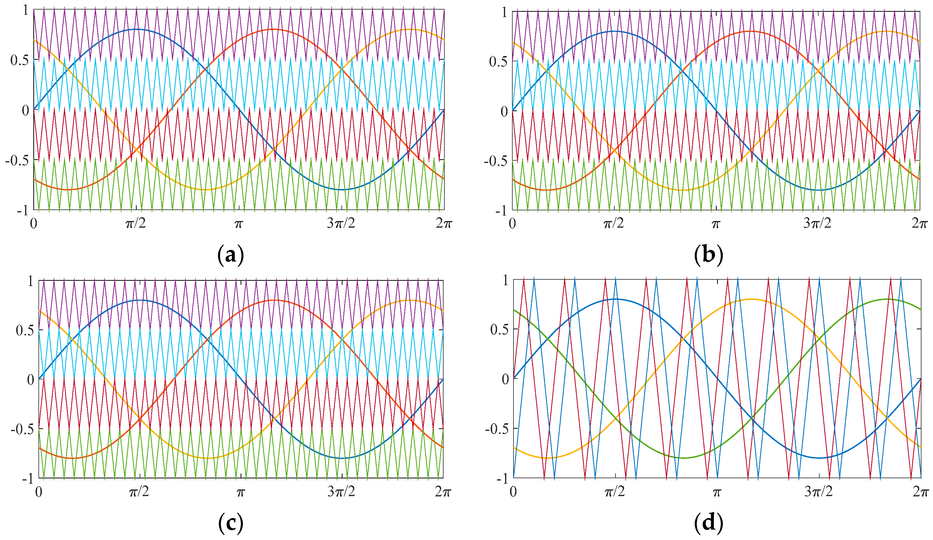
Figure 4.
Proposed modulation techniques with sinusoidal reference: (a) Phase Disposition (PD); (b) Phase Opposition Disposition (POD); (c) Alternative Phase Opposition Disposition (APOD); and (d) Phase Shifted (PS). Blue, red and orange sinusoidal signals represent the reference signals; interferences with the triangular signals generate the modulation angles for the four switches.
Figure 5.
Proposed modulation techniques with THI reference: (a) Phase Disposition PD; (b) Phase Opposition Disposition POD; (c) Alternative Phase Opposition Disposition APOD; and (d) Phase Shifted PS. Blue, red and orange THI signals represent the reference signals; interferences with the triangular signals generate the modulation angles for the four switches.
Figure 6.
Proposed modulation techniques with SFO reference: (a) Phase Disposition (PD); (b) Phase Opposition Disposition (POD); (c) Alternative Phase Opposition Disposition (APOD); and (d) Phase Shifted (PS). Blue, red and orange SFO signals represent the reference signals; interferences with the triangular signals generate the modulation angles for the four switches.
Figure 7.
Block diagram of a typical grid-connected system. HMI: human–machine interface.
Figure 7.
Block diagram of a typical grid-connected system. HMI: human–machine interface.
Figure 8.
Topology structure of a three-phase five-level CHB inverter system.
Figure 8.
Topology structure of a three-phase five-level CHB inverter system.
Figure 9.
Synchronous reference frame control strategy.
Figure 9.
Synchronous reference frame control strategy.
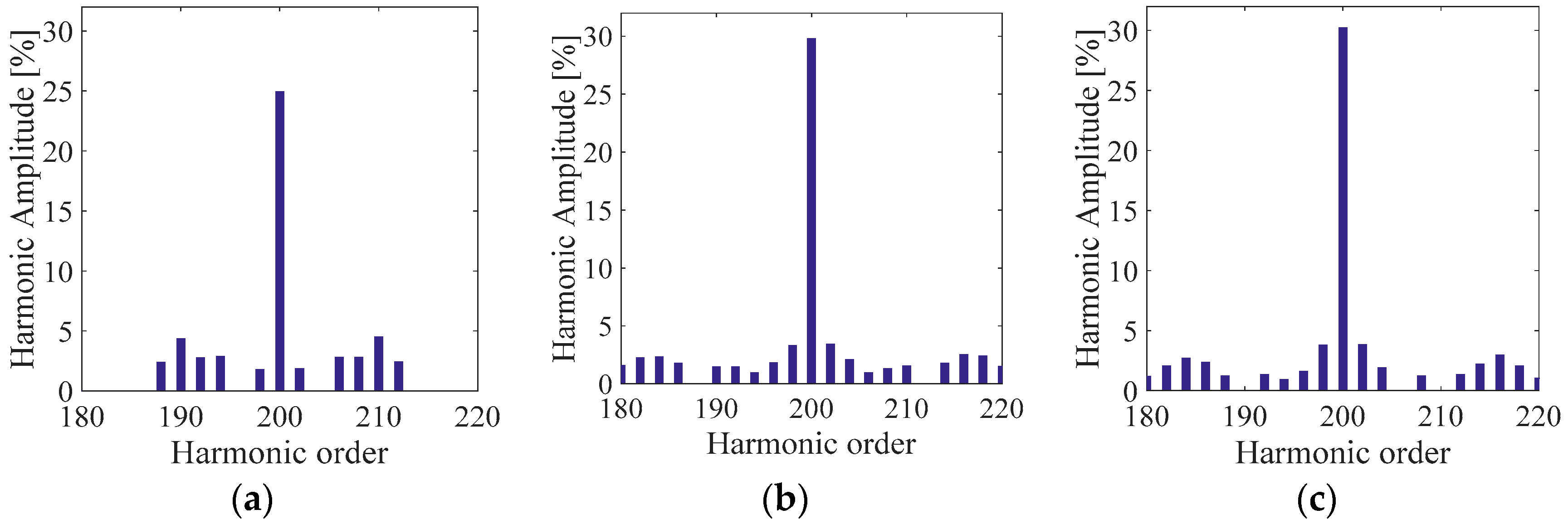
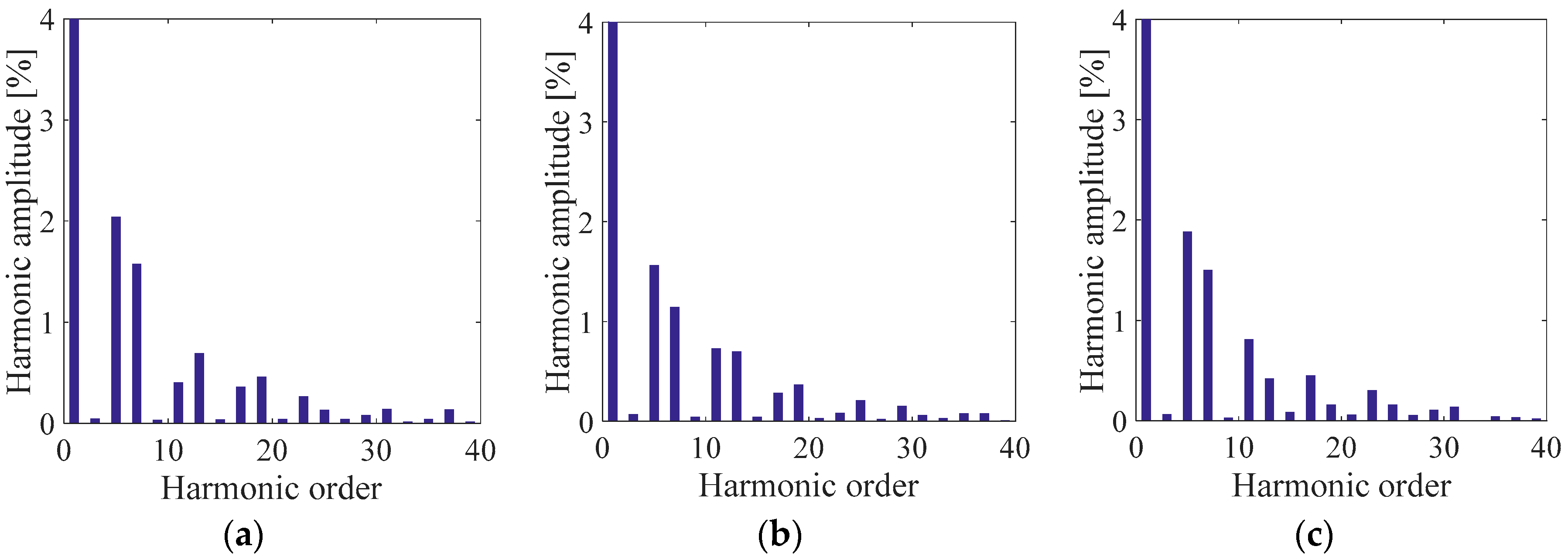
Figure 10.
Phase voltage harmonic spectra centered around the switching frequency (10kHz) in percent respect to the fundamental amplitude of (a) SPD, (b) THIPD and (c) SFOPD.
Figure 10.
Phase voltage harmonic spectra centered around the switching frequency (10kHz) in percent respect to the fundamental amplitude of (a) SPD, (b) THIPD and (c) SFOPD.
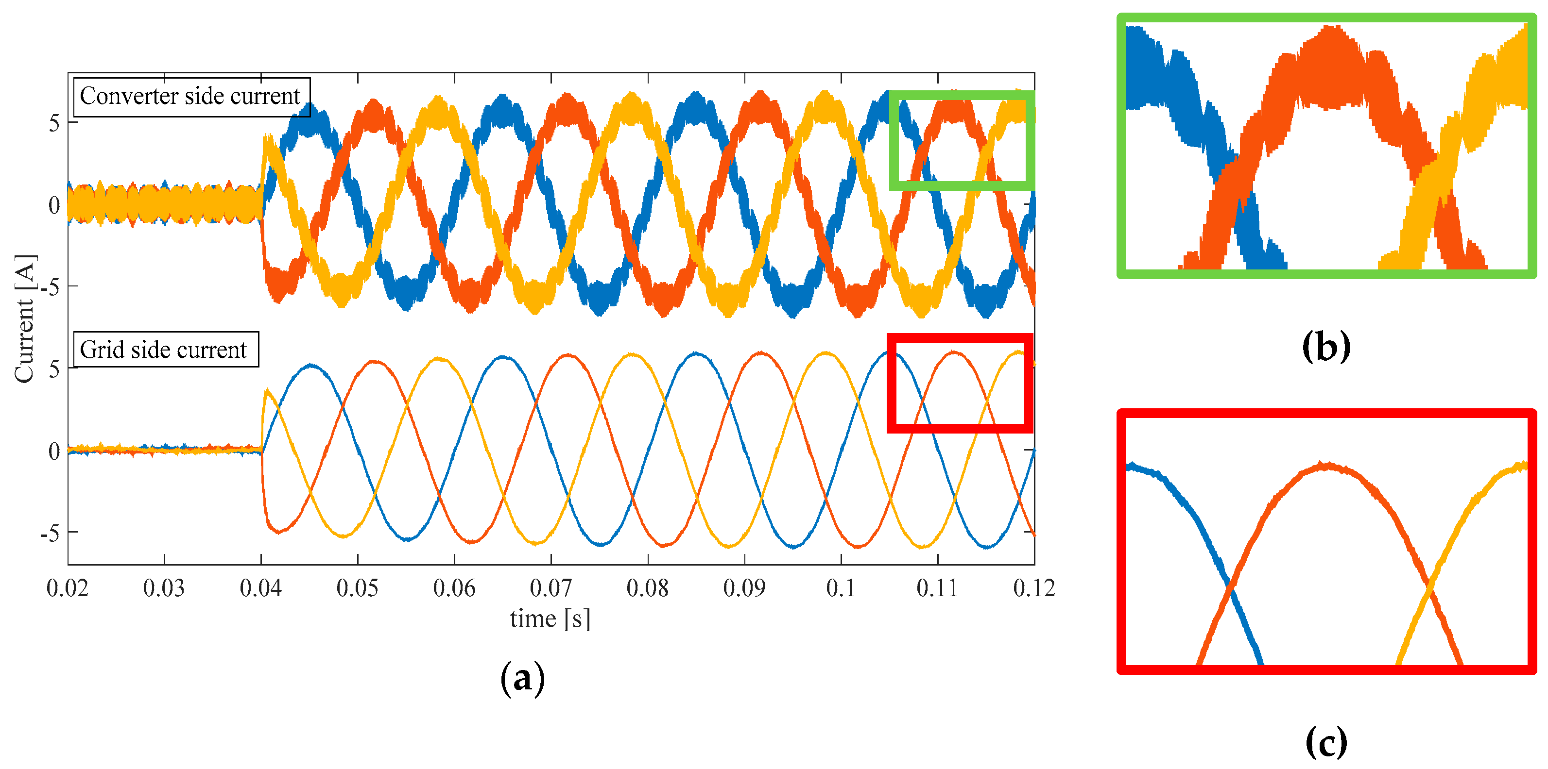
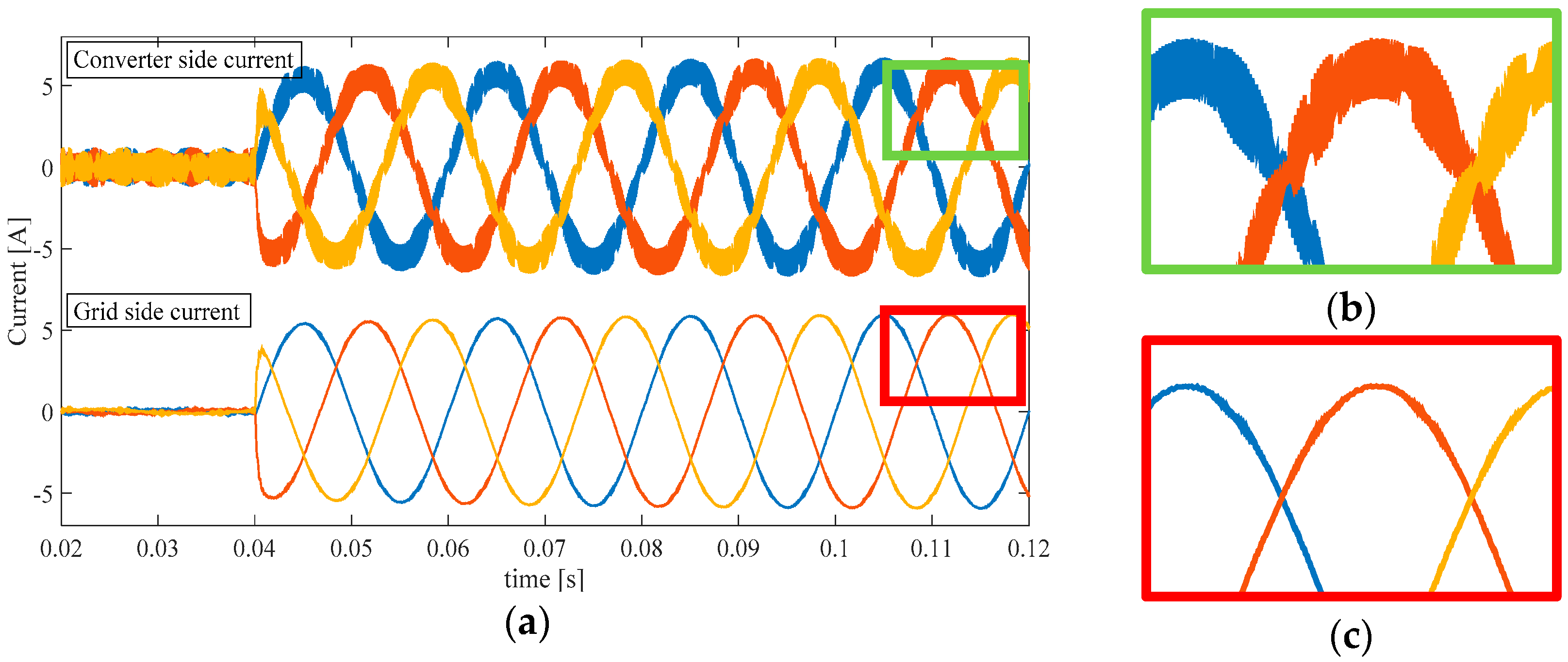
Figure 11.
Converter side and grid side three-phase current with SPD. (a) Transient behavior in multiple cycles; (b) Ripple magnification for converter side current; (c) Ripple magnification for grid side current.
Figure 11.
Converter side and grid side three-phase current with SPD. (a) Transient behavior in multiple cycles; (b) Ripple magnification for converter side current; (c) Ripple magnification for grid side current.
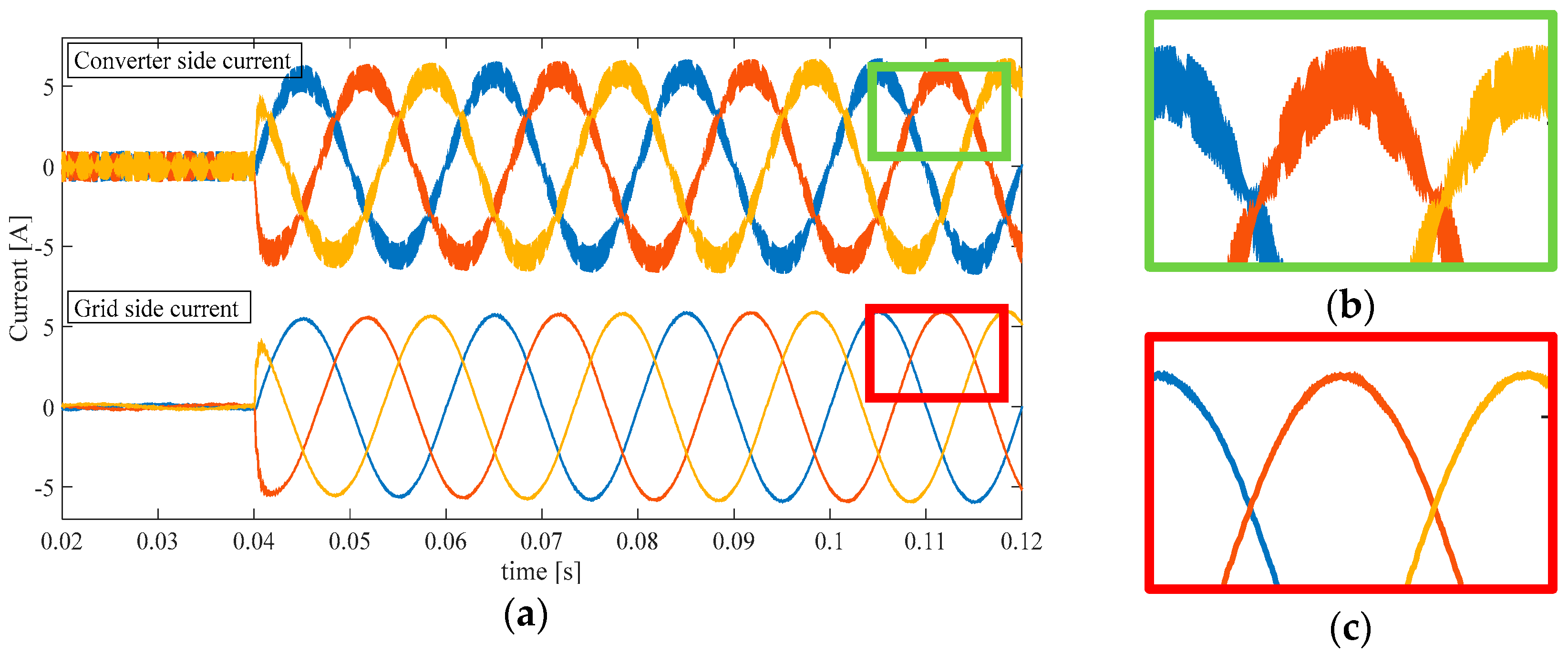
Figure 12.
Converter side and grid side three-phase current with THIPD. (a) Transient behavior in multiple cycles; (b) Ripple magnification for converter side current; (c) Ripple magnification for grid side current.
Figure 12.
Converter side and grid side three-phase current with THIPD. (a) Transient behavior in multiple cycles; (b) Ripple magnification for converter side current; (c) Ripple magnification for grid side current.
Figure 13.
Converter side and grid side three-phase current with SFOPD. (a) Transient behavior in multiple cycles; (b) Ripple magnification for converter side current; (c) Ripple magnification for grid side current.
Figure 13.
Converter side and grid side three-phase current with SFOPD. (a) Transient behavior in multiple cycles; (b) Ripple magnification for converter side current; (c) Ripple magnification for grid side current.
Figure 14.
Low order harmonics on the grid side current Iga for (a) SPD, (b) THIPD, and (c) SFOPD.
Figure 14.
Low order harmonics on the grid side current Iga for (a) SPD, (b) THIPD, and (c) SFOPD.
Figure 15.
Comparison of line voltage harmonic spectra Vab, converter side current Ia and grid side current Iga centered around the switching frequency (10 kHz) in percent respect to the fundamental amplitude for (a) SPD, (b) THIPD, and (c) SFOPD.
Figure 15.
Comparison of line voltage harmonic spectra Vab, converter side current Ia and grid side current Iga centered around the switching frequency (10 kHz) in percent respect to the fundamental amplitude for (a) SPD, (b) THIPD, and (c) SFOPD.
Figure 16.
Phase voltage harmonic spectra centered around the switching frequency (10kHz) in percent respect to the fundamental amplitude of (a) SPOD, (b) THIPOD, (c) SFOPOD, (d) SAPOD, (e) THIAPOD, and (f) SFOAPOD.
Figure 16.
Phase voltage harmonic spectra centered around the switching frequency (10kHz) in percent respect to the fundamental amplitude of (a) SPOD, (b) THIPOD, (c) SFOPOD, (d) SAPOD, (e) THIAPOD, and (f) SFOAPOD.
Figure 17.
Converter side and grid side three-phase current with SPOD. (a) Transient behavior in multiple cycles; (b) Ripple magnification for converter side current; (c) Ripple magnification for grid side current.
Figure 17.
Converter side and grid side three-phase current with SPOD. (a) Transient behavior in multiple cycles; (b) Ripple magnification for converter side current; (c) Ripple magnification for grid side current.
Figure 18.
Converter side and grid side three-phase current with THIPOD. (a) Transient behavior in multiple cycles; (b) Ripple magnification for converter side current; (c) Ripple magnification for grid side current.
Figure 18.
Converter side and grid side three-phase current with THIPOD. (a) Transient behavior in multiple cycles; (b) Ripple magnification for converter side current; (c) Ripple magnification for grid side current.
Figure 19.
Converter side and grid side three-phase current with SFOPOD. (a) Transient behavior in multiple cycles; (b) Ripple magnification for converter side current; (c) Ripple magnification for grid side current.
Figure 19.
Converter side and grid side three-phase current with SFOPOD. (a) Transient behavior in multiple cycles; (b) Ripple magnification for converter side current; (c) Ripple magnification for grid side current.
Figure 20.
Converter side and grid side three-phase current with SAPOD. (a) Transient behavior in multiple cycles; (b) Ripple magnification for converter side current; (c) Ripple magnification for grid side current.
Figure 20.
Converter side and grid side three-phase current with SAPOD. (a) Transient behavior in multiple cycles; (b) Ripple magnification for converter side current; (c) Ripple magnification for grid side current.
Figure 21.
Converter side and grid side three-phase current with THIAPOD. (a) Transient behavior in multiple cycles; (b) Ripple magnification for converter side current; (c) Ripple magnification for grid side current.
Figure 21.
Converter side and grid side three-phase current with THIAPOD. (a) Transient behavior in multiple cycles; (b) Ripple magnification for converter side current; (c) Ripple magnification for grid side current.
Figure 22.
Converter side and grid side three-phase current with SFOAPOD. (a) Transient behavior in multiple cycles; (b) Ripple magnification for converter side current; (c) Ripple magnification for grid side current.
Figure 22.
Converter side and grid side three-phase current with SFOAPOD. (a) Transient behavior in multiple cycles; (b) Ripple magnification for converter side current; (c) Ripple magnification for grid side current.
Figure 23.
Low order harmonics on the grid side current Iga for (a) SPOD, (b) THIPOD, (c) SFOPD, (d) SAPOD, (e) THIAPOD, and (f) SFOAPOD.
Figure 23.
Low order harmonics on the grid side current Iga for (a) SPOD, (b) THIPOD, (c) SFOPD, (d) SAPOD, (e) THIAPOD, and (f) SFOAPOD.
Figure 24.
Comparison of line voltage harmonic spectra Vab, converter side current Ia and grid side current Iga centered around the switching frequency (10 kHz) in percent respect to the fundamental amplitude for (a) SPOD, (b) THIPOD, (c) SFOPOD, (d) SAPOD, (e) THIAPOD, and (f) SFOAPOD.
Figure 24.
Comparison of line voltage harmonic spectra Vab, converter side current Ia and grid side current Iga centered around the switching frequency (10 kHz) in percent respect to the fundamental amplitude for (a) SPOD, (b) THIPOD, (c) SFOPOD, (d) SAPOD, (e) THIAPOD, and (f) SFOAPOD.
Figure 25.
Phase voltage harmonic spectra centered around four times of the switching frequency (10 kHz) in percent respect to the fundamental amplitude of (a) SPS, (b) THIPS, and (c) SFOPS.
Figure 25.
Phase voltage harmonic spectra centered around four times of the switching frequency (10 kHz) in percent respect to the fundamental amplitude of (a) SPS, (b) THIPS, and (c) SFOPS.
Figure 26.
Converter side and grid side three-phase current with SPS. (a) Transient behavior in multiple cycles; (b) Ripple magnification for converter side current; (c) Ripple magnification for grid side current.
Figure 26.
Converter side and grid side three-phase current with SPS. (a) Transient behavior in multiple cycles; (b) Ripple magnification for converter side current; (c) Ripple magnification for grid side current.
Figure 27.
Converter side and grid side three-phase current with THIPS. (a) Transient behavior in multiple cycles; (b) Ripple magnification for converter side current; (c) Ripple magnification for grid side current.
Figure 27.
Converter side and grid side three-phase current with THIPS. (a) Transient behavior in multiple cycles; (b) Ripple magnification for converter side current; (c) Ripple magnification for grid side current.
Figure 28.
Converter side and grid side three-phase current with SFOPS. (a) Transient behavior in multiple cycles; (b) Ripple magnification for converter side current; (c) Ripple magnification for grid side current.
Figure 28.
Converter side and grid side three-phase current with SFOPS. (a) Transient behavior in multiple cycles; (b) Ripple magnification for converter side current; (c) Ripple magnification for grid side current.
Figure 29.
Low order harmonics on the grid side current Iga for (a) SPS, (b) THIPS, and (c) SFOPS.
Figure 29.
Low order harmonics on the grid side current Iga for (a) SPS, (b) THIPS, and (c) SFOPS.
Figure 30.
Comparison of line voltage harmonic spectra Vab, converter side current Ia and grid side current Iga centered around the switching frequency (10 kHz) in percent respect to the fundamental amplitude for (a) SPS, (b) THIPS, and (c) SFOPS.
Figure 30.
Comparison of line voltage harmonic spectra Vab, converter side current Ia and grid side current Iga centered around the switching frequency (10 kHz) in percent respect to the fundamental amplitude for (a) SPS, (b) THIPS, and (c) SFOPS.
Figure 31.
A photograph of the test bench.
Figure 31.
A photograph of the test bench.
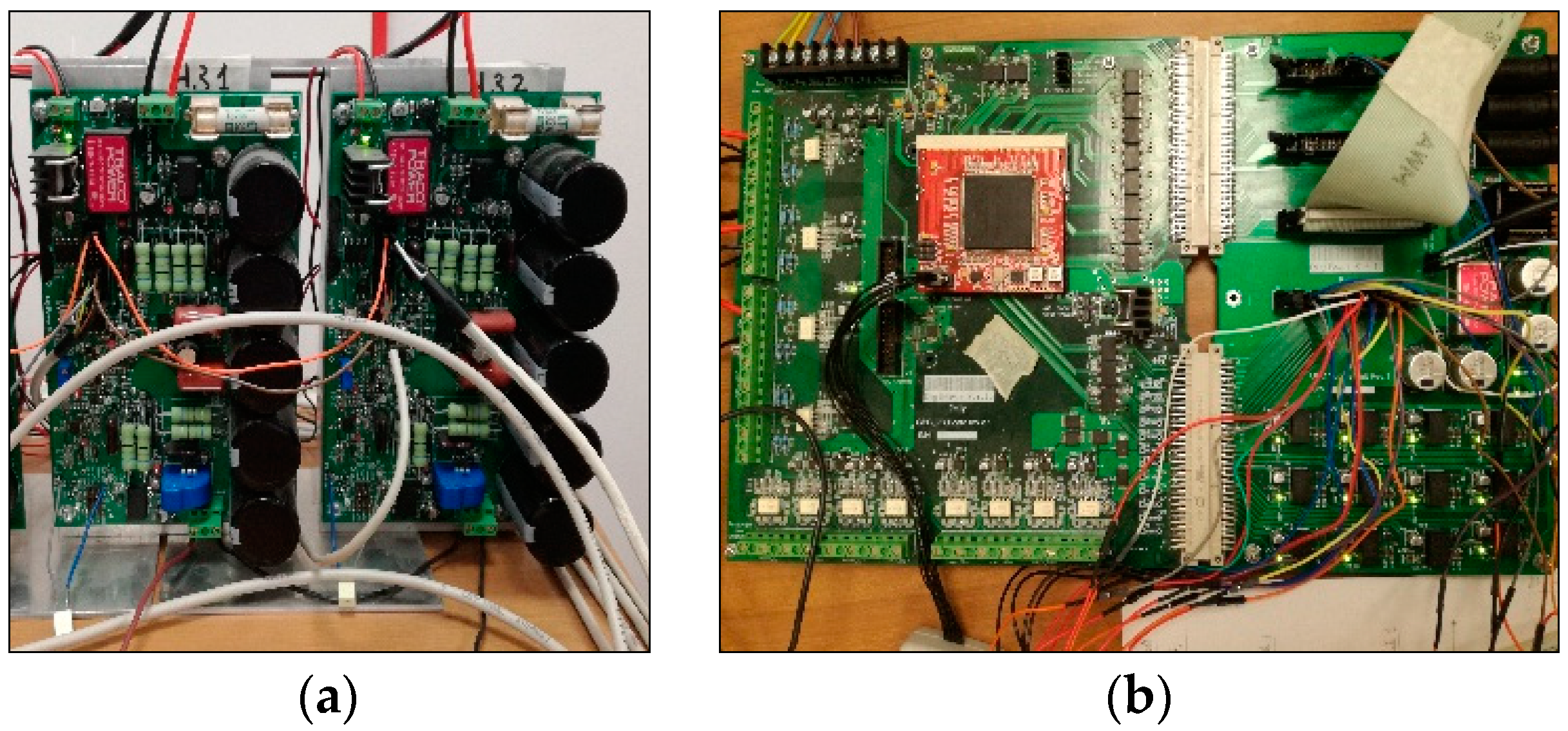
Figure 32.
A photograph of the prototype (a) H-Brides and (b) field programmable gate array (FPGA) control board.
Figure 32.
A photograph of the prototype (a) H-Brides and (b) field programmable gate array (FPGA) control board.
Figure 33.
Tree-phase LCL filter.
Figure 33.
Tree-phase LCL filter.
Figure 34.
Schematic block diagram of the control algorithm.
Figure 34.
Schematic block diagram of the control algorithm.
Figure 35.
Equivalent schematic block diagram of the PLL. PI: proportional-integral; I: integral.
Figure 35.
Equivalent schematic block diagram of the PLL. PI: proportional-integral; I: integral.
Figure 36.
Experimental PLL effectiveness.
Figure 36.
Experimental PLL effectiveness.
Figure 37.
Execution time of the current control scheme.
Figure 37.
Execution time of the current control scheme.
Figure 38.
Screenshot of the schematic block diagram of the pulse width modulation (PWM) modulator implemented in Quartus II environment for SPD modulation technique.
Figure 38.
Screenshot of the schematic block diagram of the pulse width modulation (PWM) modulator implemented in Quartus II environment for SPD modulation technique.
Figure 39.
Logic circuit to generate the gate signals with dead time.
Figure 39.
Logic circuit to generate the gate signals with dead time.
Figure 40.
Simulation of the “PWM generator” in ModelSim environment.
Figure 40.
Simulation of the “PWM generator” in ModelSim environment.
Figure 41.
Experimental validation between gate signals of the same leg.
Figure 41.
Experimental validation between gate signals of the same leg.
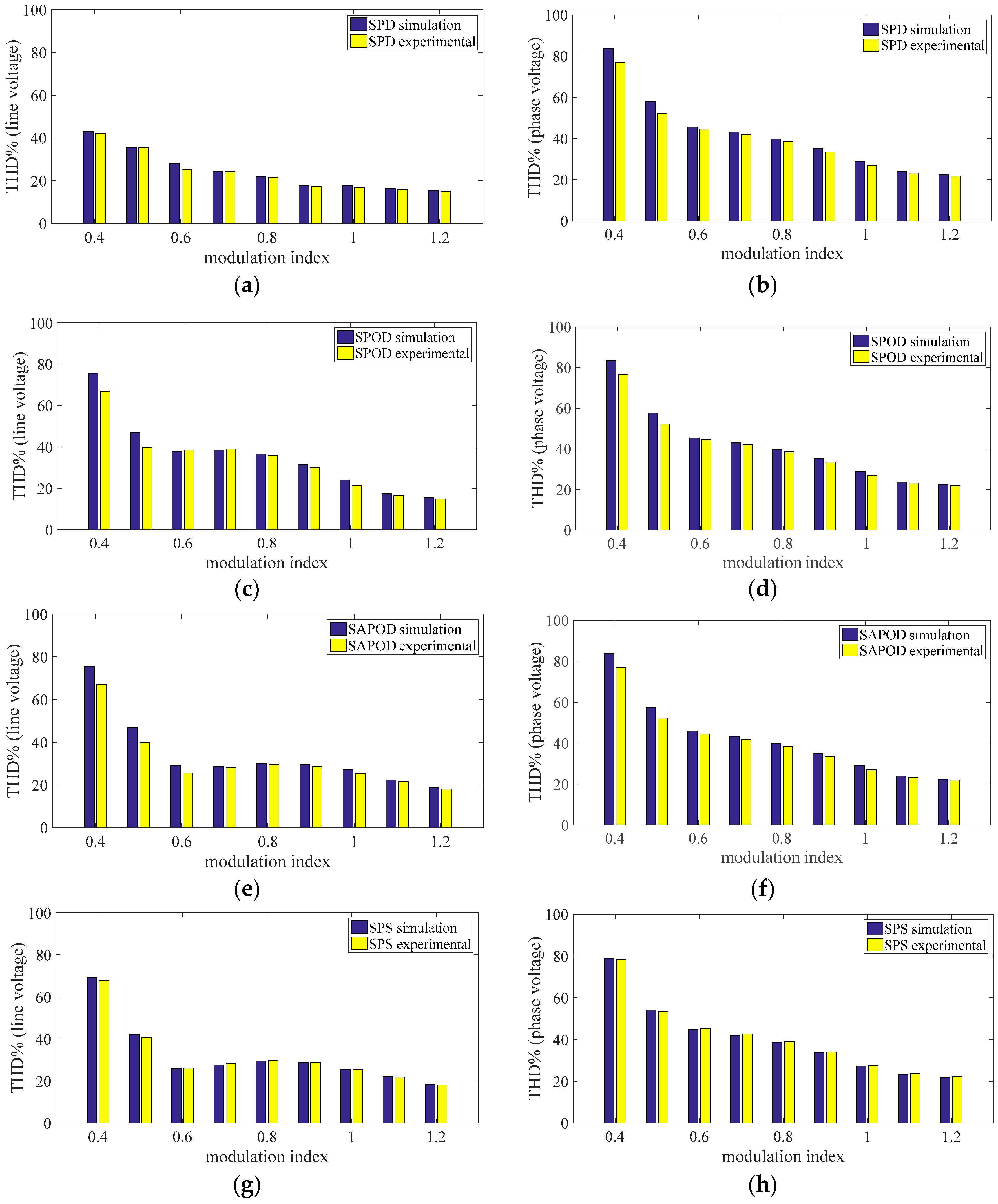
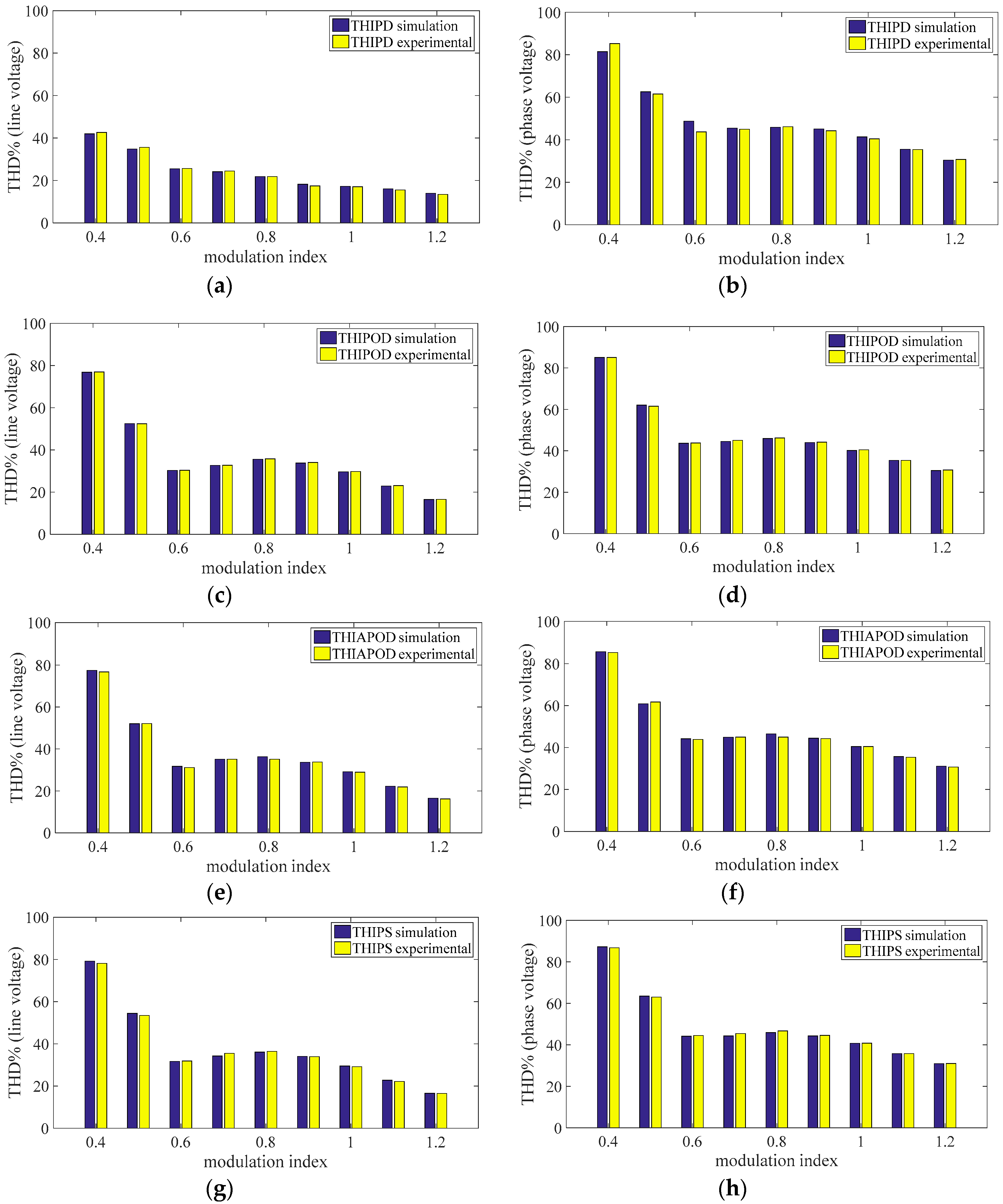
Figure 42.
Comparison between the simulated (blue) and the experimental (yellow) THD% values: (a) SPD line voltage, (b) SPD phase voltage, (c) SPOD line voltage, (d) SPOD phase voltage, (e) SAPOD line voltage, (f) SAPOD phase voltage, (g) SPS line voltage, and (h) SPS phase voltage.
Figure 42.
Comparison between the simulated (blue) and the experimental (yellow) THD% values: (a) SPD line voltage, (b) SPD phase voltage, (c) SPOD line voltage, (d) SPOD phase voltage, (e) SAPOD line voltage, (f) SAPOD phase voltage, (g) SPS line voltage, and (h) SPS phase voltage.
Figure 43.
Comparison between the simulated (blue) and the experimental (yellow) THD% values: (a) THIPD line voltage, (b) THIPD phase voltage, (c) THIPOD line voltage, (d) THIPOD phase voltage, (e) THIAPOD line voltage, (f) THIAPOD phase voltage, (g) THIPS line voltage, and (h) THIPS phase voltage.
Figure 43.
Comparison between the simulated (blue) and the experimental (yellow) THD% values: (a) THIPD line voltage, (b) THIPD phase voltage, (c) THIPOD line voltage, (d) THIPOD phase voltage, (e) THIAPOD line voltage, (f) THIAPOD phase voltage, (g) THIPS line voltage, and (h) THIPS phase voltage.
Figure 44.
Comparison between the simulated (blue) and the experimental (yellow) THD% values: (a) SFOPD line voltage, (b) SFOPD phase voltage, (c) SFOPOD line voltage, (d) SFOPOD phase voltage, (e) SFOAPOD line voltage, (f) SFOAPOD phase voltage, (g) SFOPS line voltage, and (h) SFOPS phase voltage.
Figure 44.
Comparison between the simulated (blue) and the experimental (yellow) THD% values: (a) SFOPD line voltage, (b) SFOPD phase voltage, (c) SFOPOD line voltage, (d) SFOPOD phase voltage, (e) SFOAPOD line voltage, (f) SFOAPOD phase voltage, (g) SFOPS line voltage, and (h) SFOPS phase voltage.
Figure 45.
Comparison between the experimental THD% results: (a) Sinusoidal line voltage, (b) Sinusoidal phase voltage, (c) THI line voltage, (d) THI phase voltage, (e) SFO line voltage, and (f) SFO phase voltage.
Figure 45.
Comparison between the experimental THD% results: (a) Sinusoidal line voltage, (b) Sinusoidal phase voltage, (c) THI line voltage, (d) THI phase voltage, (e) SFO line voltage, and (f) SFO phase voltage.
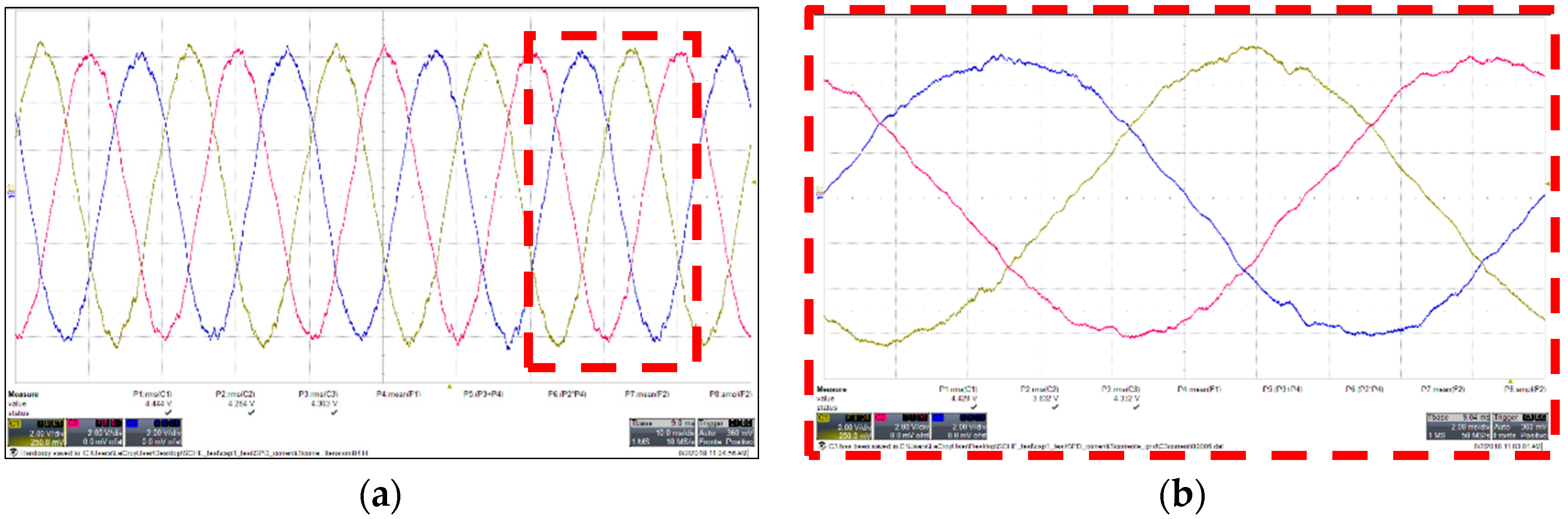
Figure 46.
Measured grid voltages (20 V/div) and grid currents (5 A/div) of the phase a and b obtained with SPD at the rated power.
Figure 46.
Measured grid voltages (20 V/div) and grid currents (5 A/div) of the phase a and b obtained with SPD at the rated power.
Figure 47.
Measured converter side currents (2 A/div) obtained with SPD at the rated power. (a) Ripple in different cycles; (b) Magnification of ripple.
Figure 47.
Measured converter side currents (2 A/div) obtained with SPD at the rated power. (a) Ripple in different cycles; (b) Magnification of ripple.
Figure 48.
Measured grid side currents (2 A/div) obtained with SPD at the rated power. (a) Ripple in different cycles; (b) Magnification of ripple.
Figure 48.
Measured grid side currents (2 A/div) obtained with SPD at the rated power. (a) Ripple in different cycles; (b) Magnification of ripple.
Figure 49.
Calculated (a) low order harmonics of the grid side current and (b) switching frequency harmonics spectra of the converter side and grid side currents.
Figure 49.
Calculated (a) low order harmonics of the grid side current and (b) switching frequency harmonics spectra of the converter side and grid side currents.
Figure 50.
Measured line voltage of the converter at rated power.
Figure 50.
Measured line voltage of the converter at rated power.
Figure 51.
Measured capacitor voltage of the LCL filter at rated power.
Figure 51.
Measured capacitor voltage of the LCL filter at rated power.
Figure 52.
Measured grid voltages (20 V/div) and grid currents (5 A/div) of the phase a and b obtained with SPS at the rated power.
Figure 52.
Measured grid voltages (20 V/div) and grid currents (5 A/div) of the phase a and b obtained with SPS at the rated power.
Figure 53.
Measured converter side currents (2 A/div) obtained with SPS at the rated power. (a) Ripple in different cycles; (b) Magnification of ripple.
Figure 53.
Measured converter side currents (2 A/div) obtained with SPS at the rated power. (a) Ripple in different cycles; (b) Magnification of ripple.
Figure 54.
Measured grid side currents (2 A/div) obtained with SPS at the rated power. (a) Ripple in different cycles; (b) Magnification of ripple.
Figure 54.
Measured grid side currents (2 A/div) obtained with SPS at the rated power. (a) Ripple in different cycles; (b) Magnification of ripple.
Figure 55.
Calculated (a) low order harmonics of the grid side current and (b) switching frequency harmonics spectra of the converter side and grid side currents.
Figure 55.
Calculated (a) low order harmonics of the grid side current and (b) switching frequency harmonics spectra of the converter side and grid side currents.
Figure 56.
Measured line voltage of the converter at rated power.
Figure 56.
Measured line voltage of the converter at rated power.
Figure 57.
Measured capacitor voltage of the LCL filter at rated power.
Figure 57.
Measured capacitor voltage of the LCL filter at rated power.
Table 1.
Current harmonic limits.
Table 1.
Current harmonic limits.
| Harmonic Order, h | Limit in % of Rated Current |
|---|
| h < 11 | 4.0 |
| 11 ≤ h < 17 | 2.0 |
| 17 ≤ h < 23 | 1.5 |
| 23 ≤ h < 35 | 0.6 |
| h ≥ 35 | 0.3 |
Table 2.
Grid side inductance values.
Table 2.
Grid side inductance values.
| | PD | POD | APOD | PS |
|---|
| Sine | 0.260 mH | 0.882 mH | 0.530 mH | 0.371 mH |
| THI | 0.222 mH | 1.938 mH | 0.584 mH | 0.393 mH |
| SFO | 0.260 mH | 0.882 mH | 0.530 mH | 0.371 mH |
Table 3.
Current Ripple, r and x values.
Table 3.
Current Ripple, r and x values.
| | Sine | THI | SFO |
|---|
| r | x% | ig/i | r | x% | ig/i | r | x% | ig/i |
|---|
| PD | 1.40 | 1.94% | 10.09% | 1.40 | 2.38% | 10.29% | 1.20 | 2.38% | 10.03% |
| POD | 0.40 | 1.94% | 10.21% | 0.10 | 3.25% | 10.85% | 0.40 | 1.94% | 10.21% |
| APOD | 0.90 | 1.50% | 10.81% | 0.60 | 1.94% | 10.51% | 0.90 | 1.50% | 10.18% |
| PS | 1.00 | 1.94% | 10.21% | 1.20 | 1.50% | 10.65% | 1.00 | 1.94% | 10.21% |
Table 4.
LCL filters parameters and frequency resonant.
Table 4.
LCL filters parameters and frequency resonant.
| | L (mH) | Cf (μF) | L*g (mH) | Lg (mH) |
|---|
| SPD | 0.260 | 8.04 | 0.365 | 0.257 |
| SPOD | 0.882 | 8.04 | 0.352 | 0.244 |
| SAPOD | 0.530 | 6.21 | 0.477 | 0.369 |
| SPS | 0.371 | 8.04 | 0.371 | 0.263 |
| THIPD | 0.222 | 9.86 | 0.311 | 0.203 |
| THIPOD | 1.938 | 13.47 | 0.193 | 0.085 |
| THIAPOD | 0.584 | 8.04 | 0.350 | 0.242 |
| THIPS | 0.393 | 6.21 | 0.471 | 0.363 |
| SFOPD | 0.260 | 9.86 | 0.313 | 0.204 |
| SFOPOD | 0.882 | 8.04 | 0.352 | 0.244 |
| SFOAPOD | 0.530 | 6.21 | 0.424 | 0.316 |
| SFOPS | 0.371 | 8.04 | 0.371 | 0.263 |
Table 5.
Limits on the LCL parameter values.
Table 5.
Limits on the LCL parameter values.
| | ΣL (p.u.) | x (%) | fres (kHz) |
|---|
| SPD | 0.025 | 1.94% | 4.54 |
| SPOD | 0.050 | 1.94% | 3.53 |
| SAPOD | 0.041 | 1.50% | 4.02 |
| SPS | 0.030 | 1.94% | 4.11 |
| THIPD | 0.021 | 2.38% | 4.44 |
| THIPOD | 0.087 | 3.25% | 3.26 |
| THIAPOD | 0.038 | 1.94% | 3.79 |
| THIPS | 0.035 | 1.50% | 4.35 |
| SFOPD | 0.023 | 2.38% | 4.24 |
| SFOPOD | 0.050 | 1.94% | 3.53 |
| SFOAPOD | 0.039 | 1.50% | 4.15 |
| SFOPS | 0.030 | 1.94% | 4.11 |
Table 6.
PI regulator parameters.
Table 6.
PI regulator parameters.
| | Sine | THI | SFO |
|---|
| kp | TI (ms) | ki | kp | TI (ms) | ki | kp | TI (ms) | ki |
|---|
| PD | 2.09 | 15.65 | 133.73 | 1.78 | 13.36 | 133.73 | 1.91 | 14.35 | 133.73 |
| POD | 4.12 | 30.88 | 133.73 | 7.11 | 53.31 | 133.73 | 4.11 | 30.88 | 133.73 |
| APOD | 3.36 | 25.20 | 133.73 | 3.12 | 23.36 | 133.73 | 3.18 | 23.87 | 133.73 |
| PS | 2.48 | 18.58 | 133.73 | 2.88 | 21.63 | 133.73 | 2.48 | 18.58 | 133.73 |
Table 7.
Simulation parameters.
Table 7.
Simulation parameters.
| Electric parameter | Value |
|---|
| Grid line Voltage | 50 V |
| Rated current | 6 A |
| Grid frequency | 50 Hz |
| DC Voltages | 24 V |
| Switching frequency | 10 kHz |
| Inductance and resistance of the transformer (low side reported) | 108.23 μH 25 mΩ |
Table 8.
Partial Total Harmonic Distortion” (PTHD%) values obtained with SPD, THIPD, and SFOPD.
Table 8.
Partial Total Harmonic Distortion” (PTHD%) values obtained with SPD, THIPD, and SFOPD.
| | Vab | Ia | Iga |
|---|
| SPD | 7.94% | 3.92% | 0.38% |
| THIPD | 7.86% | 4.61% | 0.43% |
| SFOPD | 8.29% | 4.08% | 0.38% |
Table 9.
PTHD% values obtained with SPOD, THIPOD, SFOPD, SAPOD, THIAPOD, and SFOAPOD.
Table 9.
PTHD% values obtained with SPOD, THIPOD, SFOPD, SAPOD, THIAPOD, and SFOAPOD.
| | Vab | Ia | Iga |
|---|
| SPOD | 25.62% | 3.37% | 0.33% |
| THIPOD | 29.12% | 1.72% | 0.18% |
| SFOPOD | 30.60% | 4.12% | 0.40% |
| SAPOD | 24.17% | 5.68% | 0.53% |
| THIAPOD | 29.78% | 6.16% | 0.61% |
| SFOAPOD | 30.65% | 7.21% | 0.77% |
Table 10.
PTHD% values obtained with SPS, THIPS, and SFOPS.
Table 10.
PTHD% values obtained with SPS, THIPS, and SFOPS.
| | Vab | Ia | Iga |
|---|
| SPS | 23.51% | 1.80% | 0.0095% |
| THIPS | 29.84% | 2.16% | 0.0117% |
| SFOPS | 30.51% | 2.35% | 0.0124% |
Table 11.
Technical features of the IRFB4115PBF device [
57].
Table 11.
Technical features of the IRFB4115PBF device [
57].
| Voltage Vdss | 150 V |
| Resistance Rds(on) | 9.3 mΩ |
| Current Id (silicon limited) | 104 A |
| Turn on delay tD(on) | 18 ns |
| Rise time tR | 73 ns |
| Turn off delay TD(off) | 41 ns |
| Fall time tF | 39 ns |
| Reversal recovery tRR | 86 ns |
Table 12.
Execution time of the mathematic operation in FP 32bit.
Table 12.
Execution time of the mathematic operation in FP 32bit.
| Mathematic operation | Time |
|---|
| Conversion Integer to Floating (Integer 13 bit, FP 32bit) | 60 ns |
| Sum or subtraction (FP 32 bit) | 140 ns |
| Product (FP 32 bit) | 110 ns |
Table 13.
Execution time main block of the PLL.
Table 13.
Execution time main block of the PLL.
| Operation | Time |
|---|
| ABC to DQ transformation (FP 32bit) | 880 ns |
| PI regulator (FP 32 bit) | 540 ns |
| Integral (FP 32 bit) | 270 ns |
| Overflow control and look-up table (FP 32 bit) | 450 ns |
Table 14.
Experimental THD% of the converter and grid side currents, obtained with SPD, for different values of the injected current into the grid.
Table 14.
Experimental THD% of the converter and grid side currents, obtained with SPD, for different values of the injected current into the grid.
| | In/3 | In/2 | 2In/3 | In |
|---|
| Converter side current | 12.17% | 7.82% | 6.46% | 5.88% |
| Grid side current | 7.97% | 4.78% | 4.26% | 3.72% |
Table 15.
Experimental THD% of the converter and grid side currents, obtained with SPS, for different values of the injected current into the grid.
Table 15.
Experimental THD% of the converter and grid side currents, obtained with SPS, for different values of the injected current into the grid.
| | In/3 | In/2 | 2In/3 | In |
|---|
| Converter side current | 12.28% | 8.41% | 6.80% | 5.64% |
| Grid side current | 7.42% | 4.45% | 3.91% | 3.33% |


