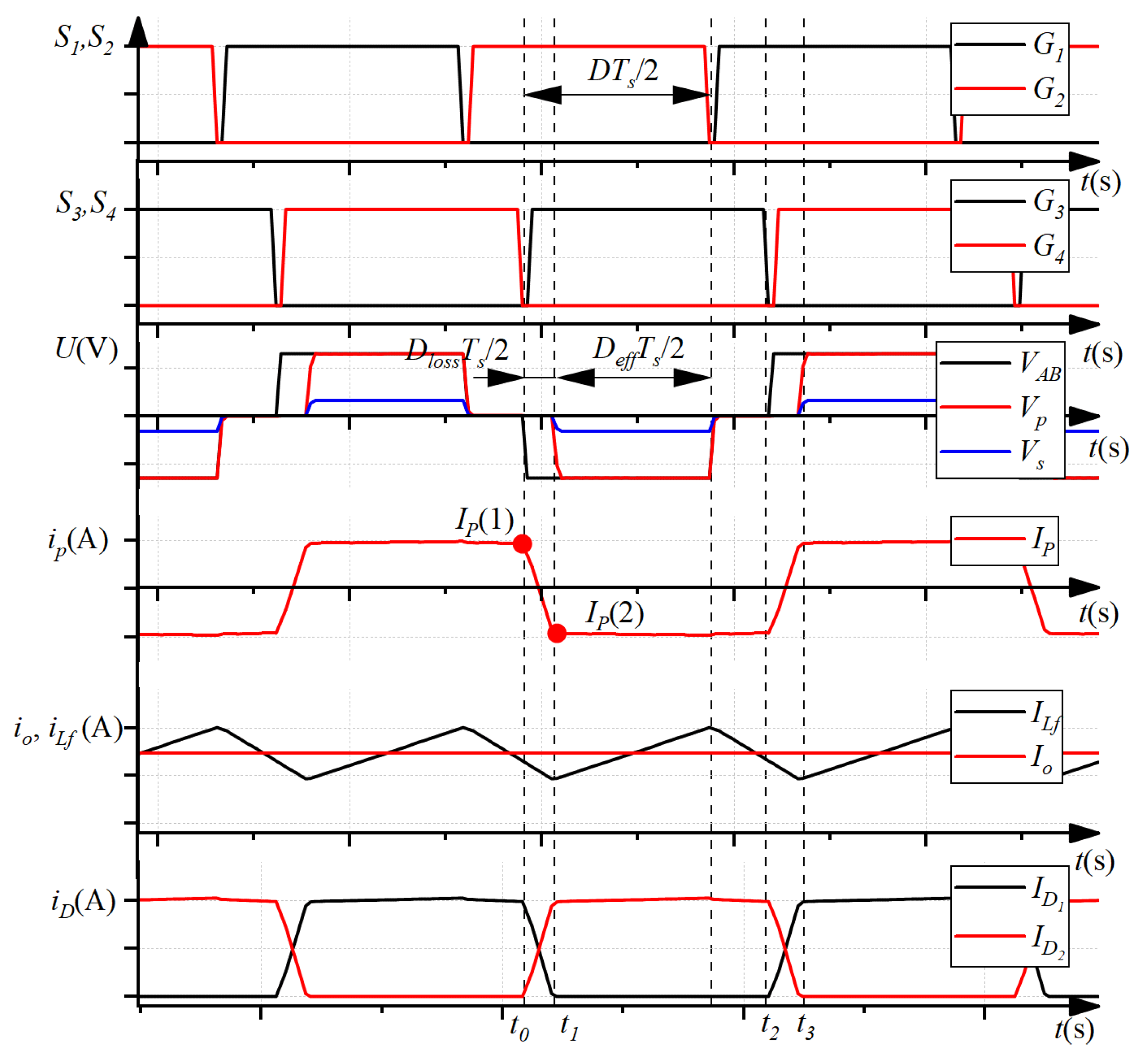
Figure 1.
Switching singles and key waveform of PSFB.
Figure 1.
Switching singles and key waveform of PSFB.
Figure 2.
Operation mode during ~.
Figure 2.
Operation mode during ~.
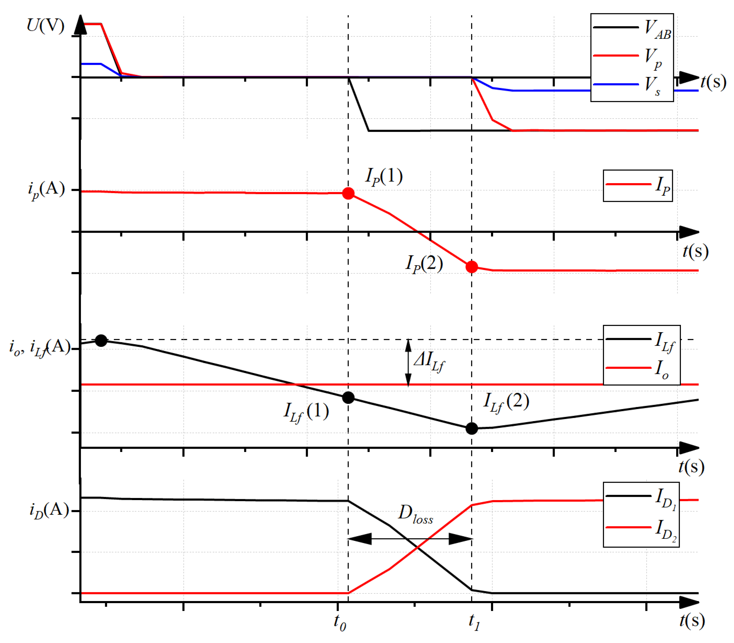
Figure 3.
Loss of duty cycle during voltage clamping of transformer windings.
Figure 3.
Loss of duty cycle during voltage clamping of transformer windings.
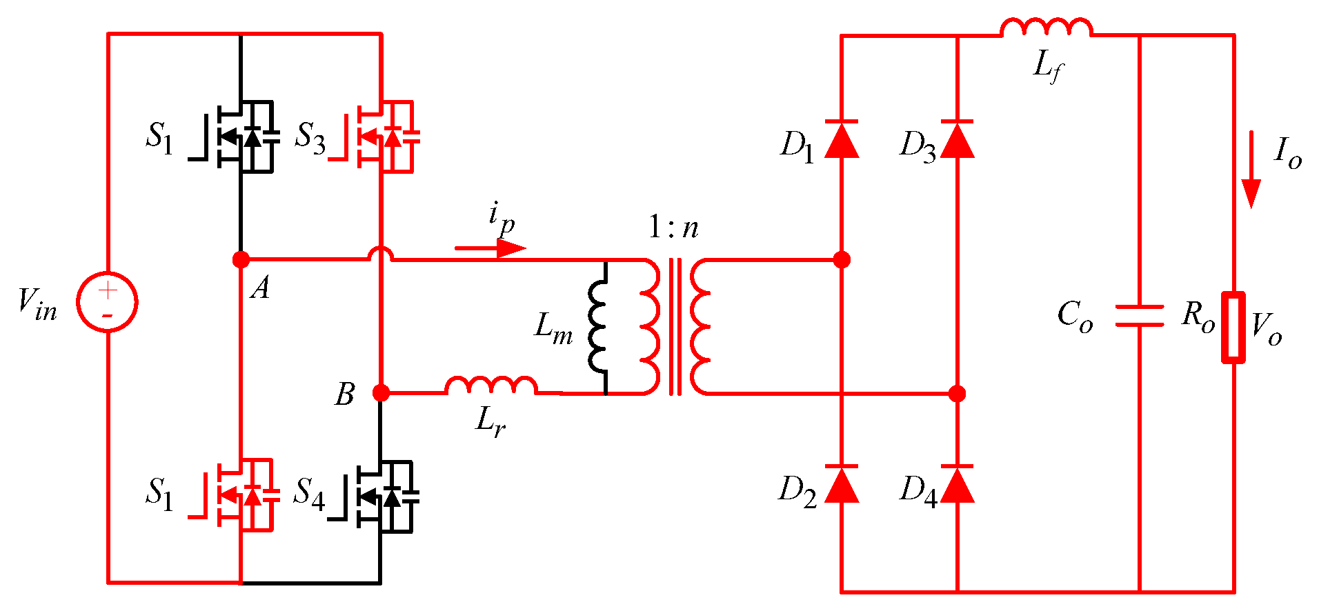
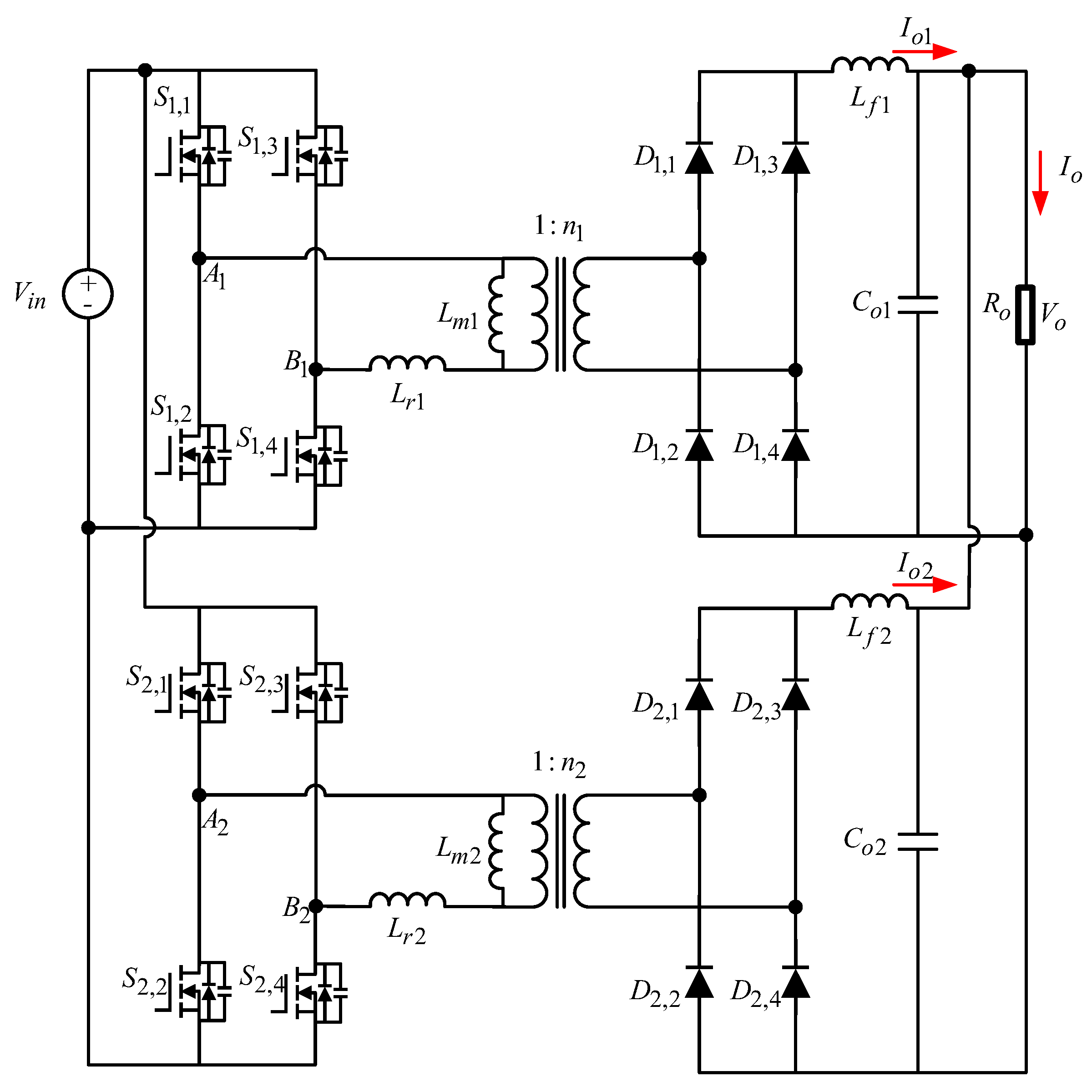
Figure 4.
Two-phase parallel PSFB converter.
Figure 4.
Two-phase parallel PSFB converter.
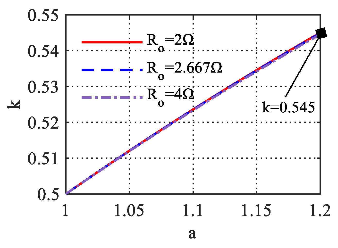
Figure 5.
Solutions of k for different values of a at different output resistances (when = 4 , = 400 W; = 2.667 , = 600 W; = 2 , = 800 W).
Figure 5.
Solutions of k for different values of a at different output resistances (when = 4 , = 400 W; = 2.667 , = 600 W; = 2 , = 800 W).
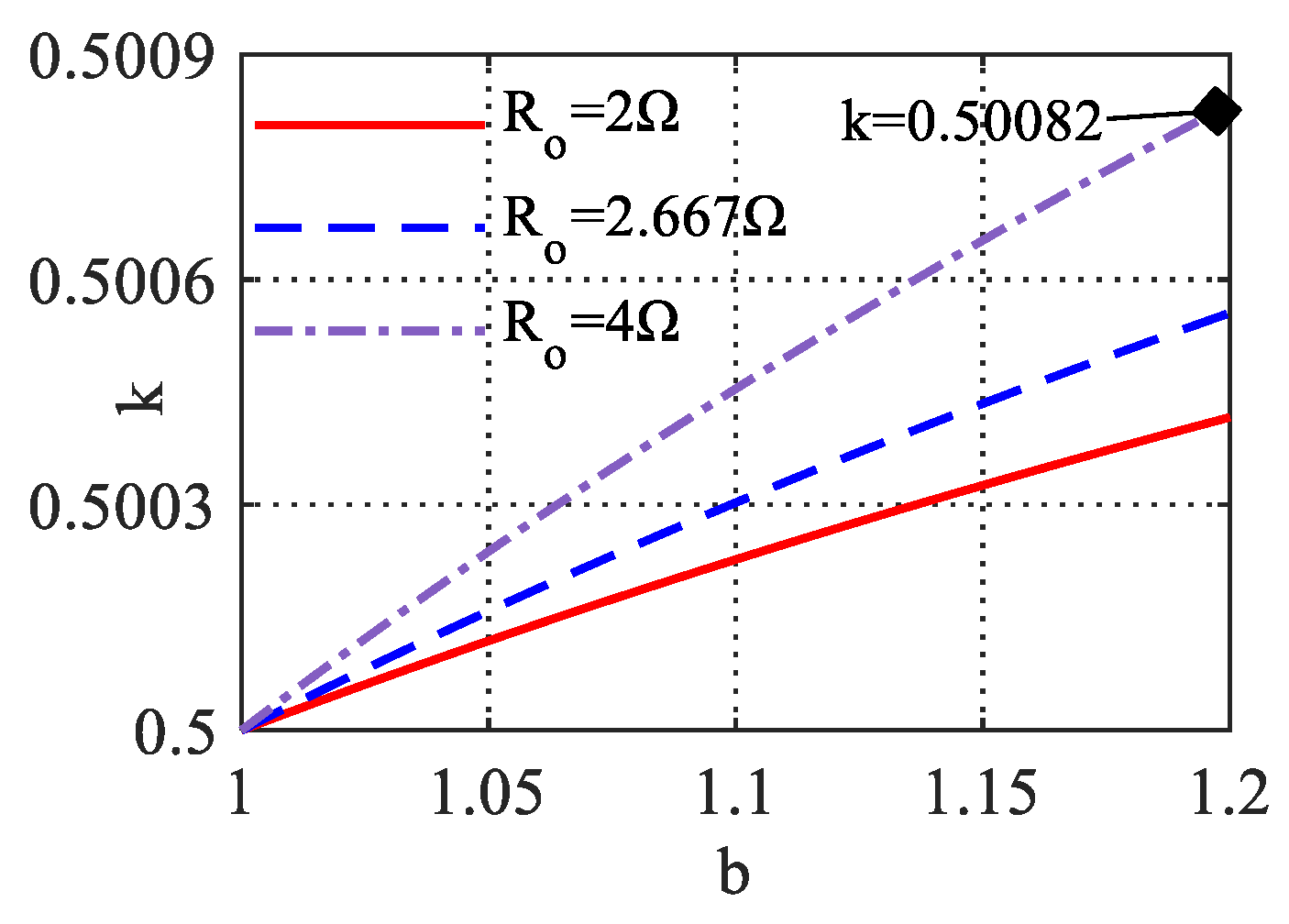
Figure 6.
Solutions of k for different values of b at different output resistances.
Figure 6.
Solutions of k for different values of b at different output resistances.
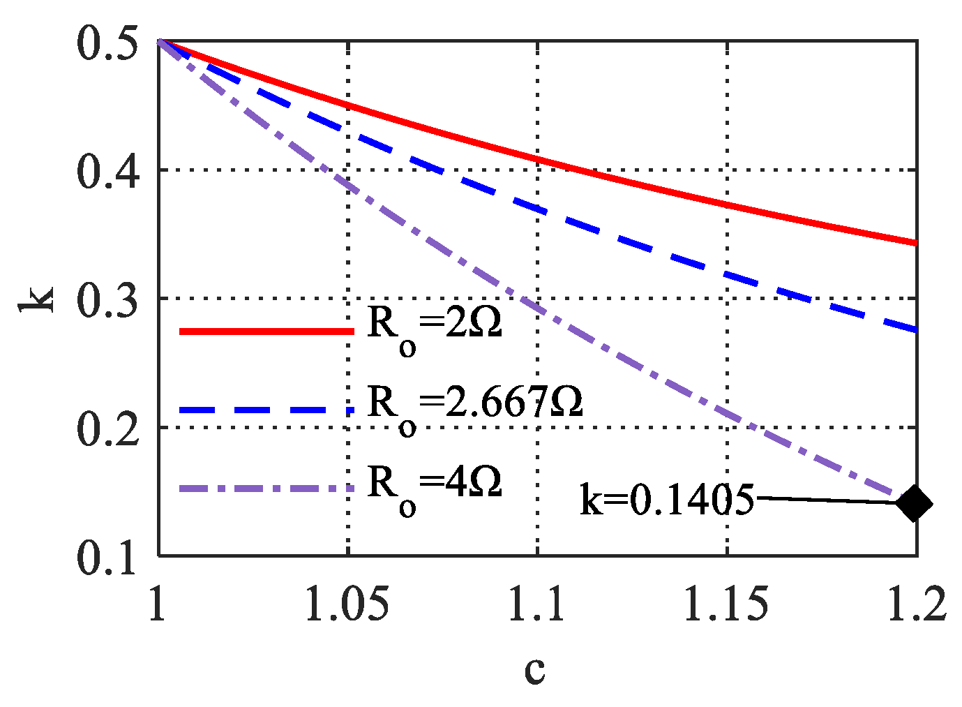
Figure 7.
Solutions of k for different values of c at different output resistances.
Figure 7.
Solutions of k for different values of c at different output resistances.
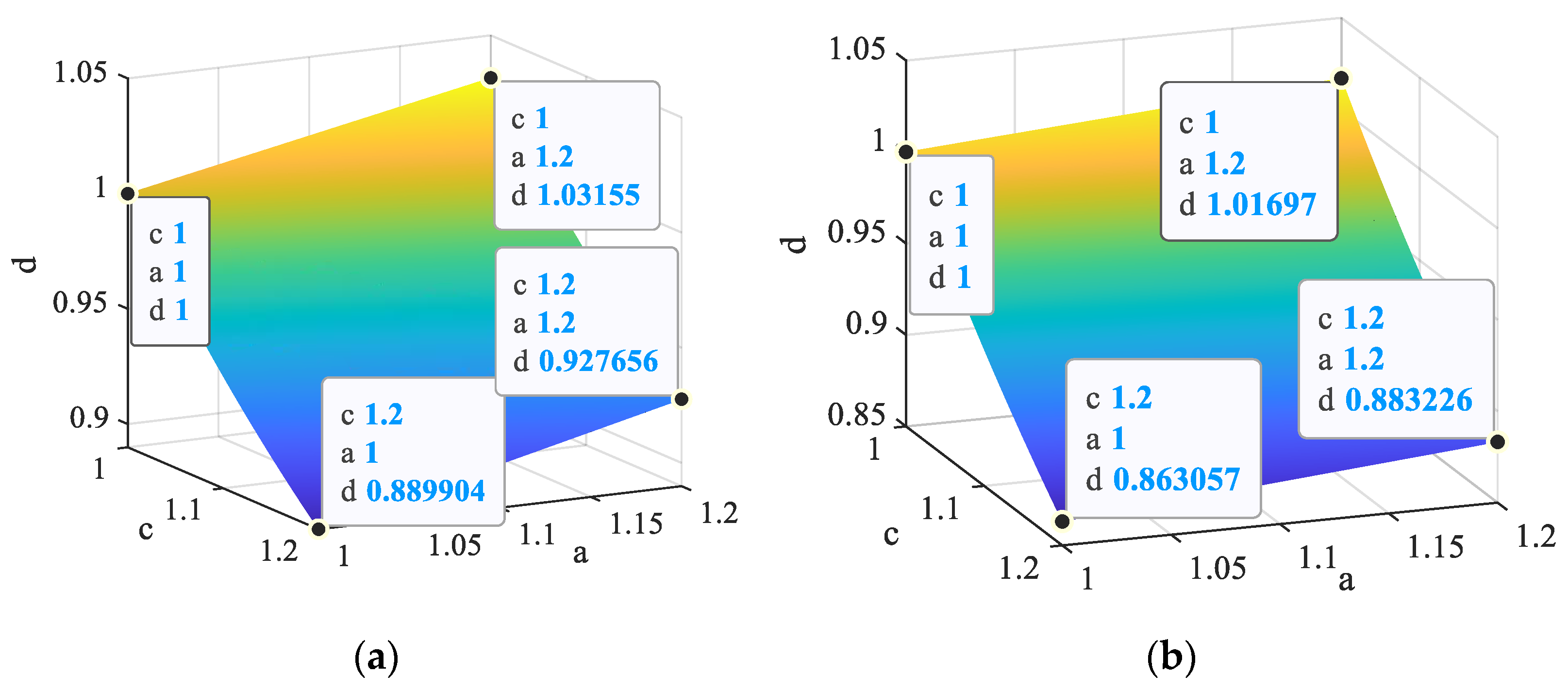
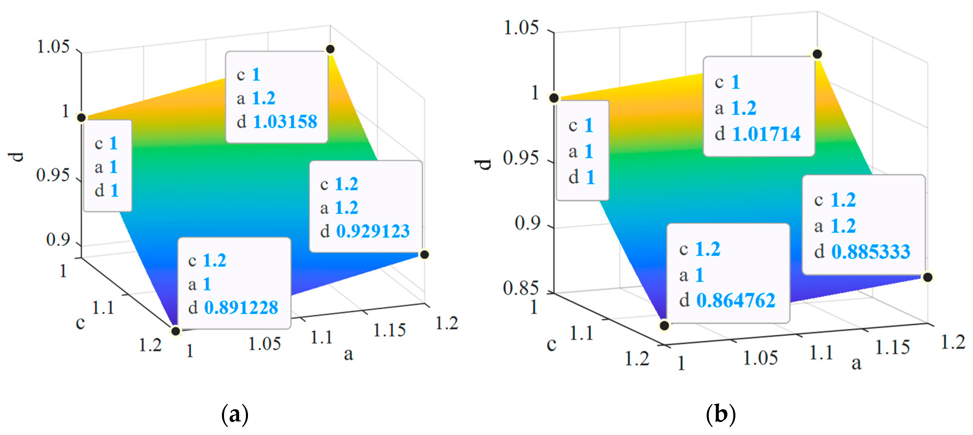
Figure 8.
Solution of phase shift duty cycle compensation d in different output resistances: (a) = 2 , = 800 W; (b) = 4 , = 400 W.
Figure 8.
Solution of phase shift duty cycle compensation d in different output resistances: (a) = 2 , = 800 W; (b) = 4 , = 400 W.
Figure 9.
Solution of d after simplifying in different output resistances: (a) = 2 , = 800 W; (b) = 4 , = 400 W.
Figure 9.
Solution of d after simplifying in different output resistances: (a) = 2 , = 800 W; (b) = 4 , = 400 W.
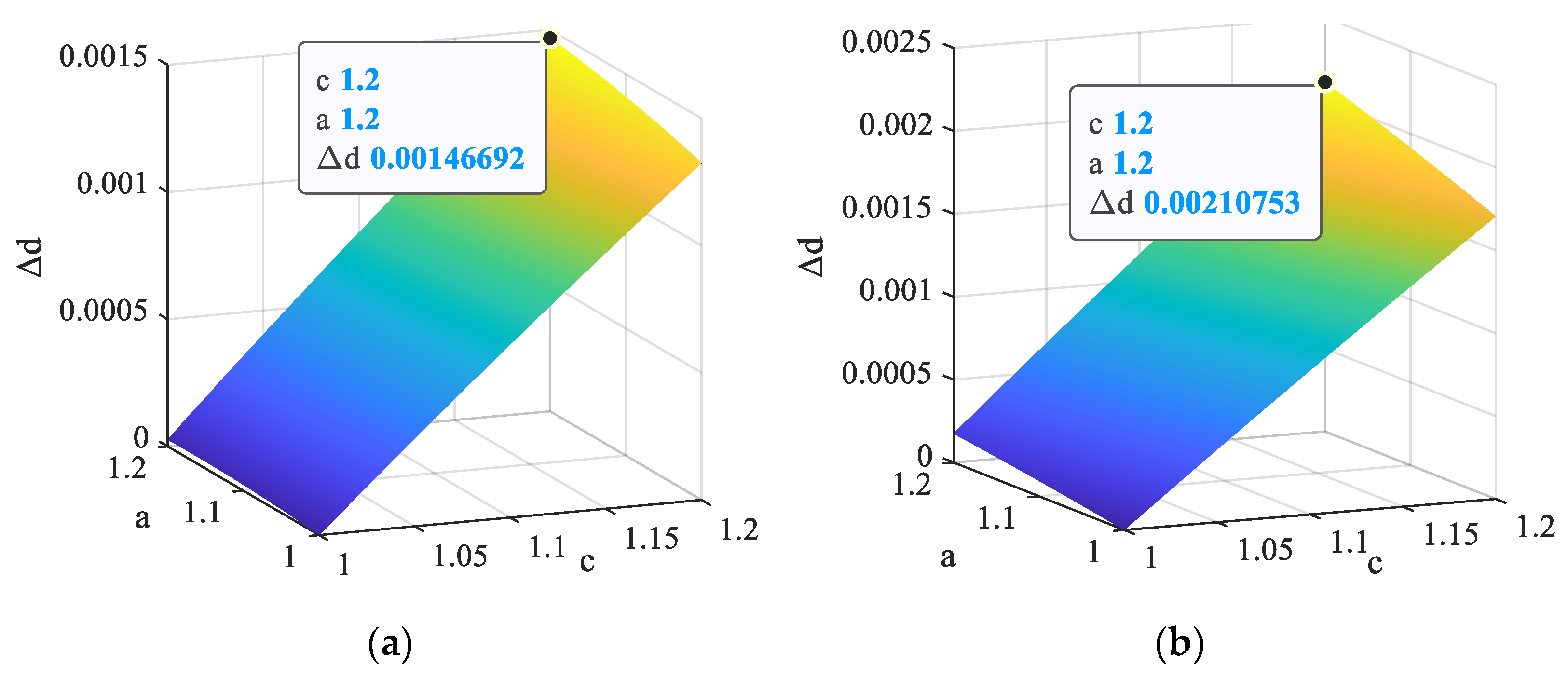
Figure 10.
Error of d base on Equation (30) in different output resistances: (a) = 2 , = 800 W; (b) = 4 , = 400 W.
Figure 10.
Error of d base on Equation (30) in different output resistances: (a) = 2 , = 800 W; (b) = 4 , = 400 W.
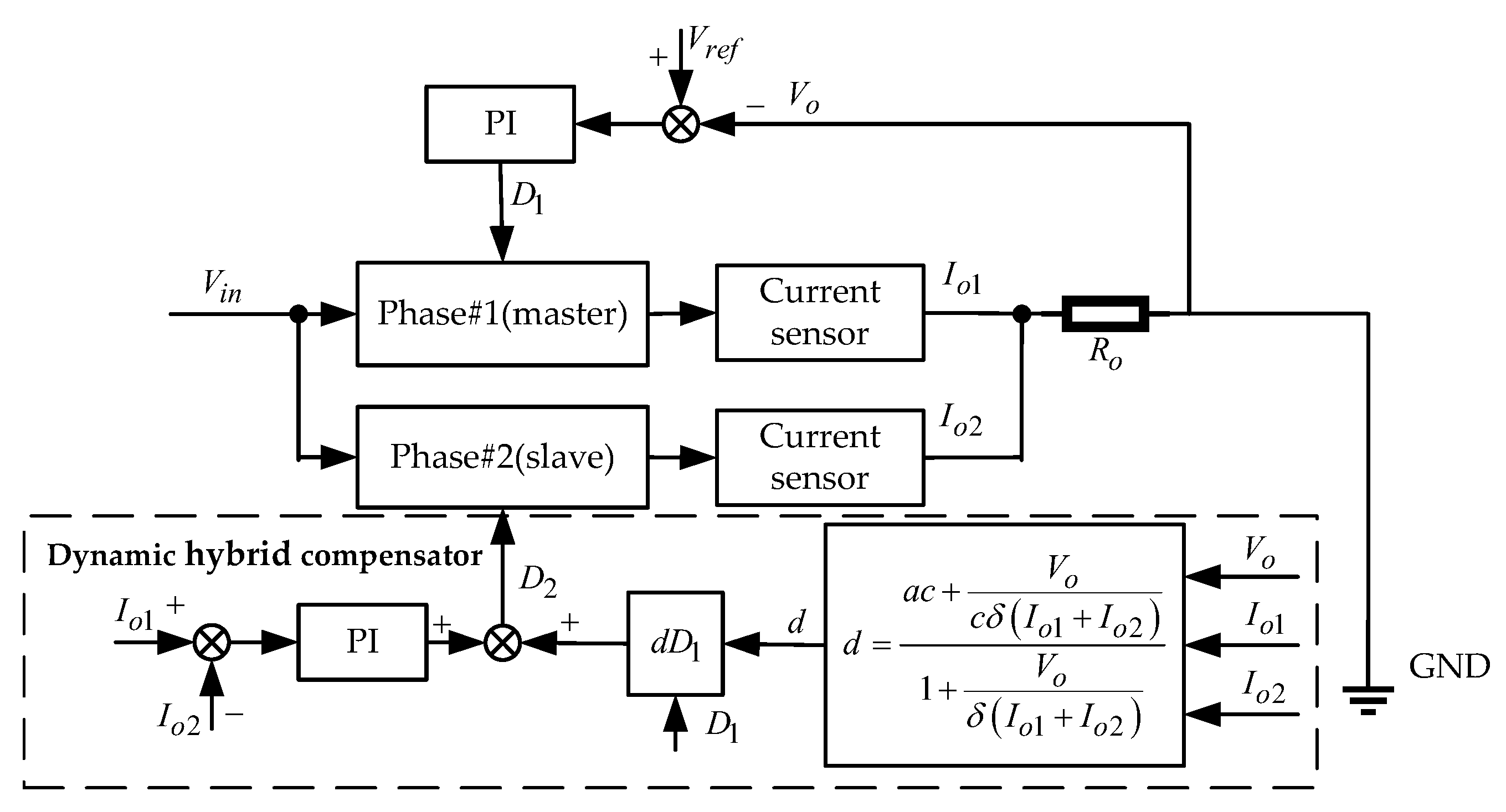
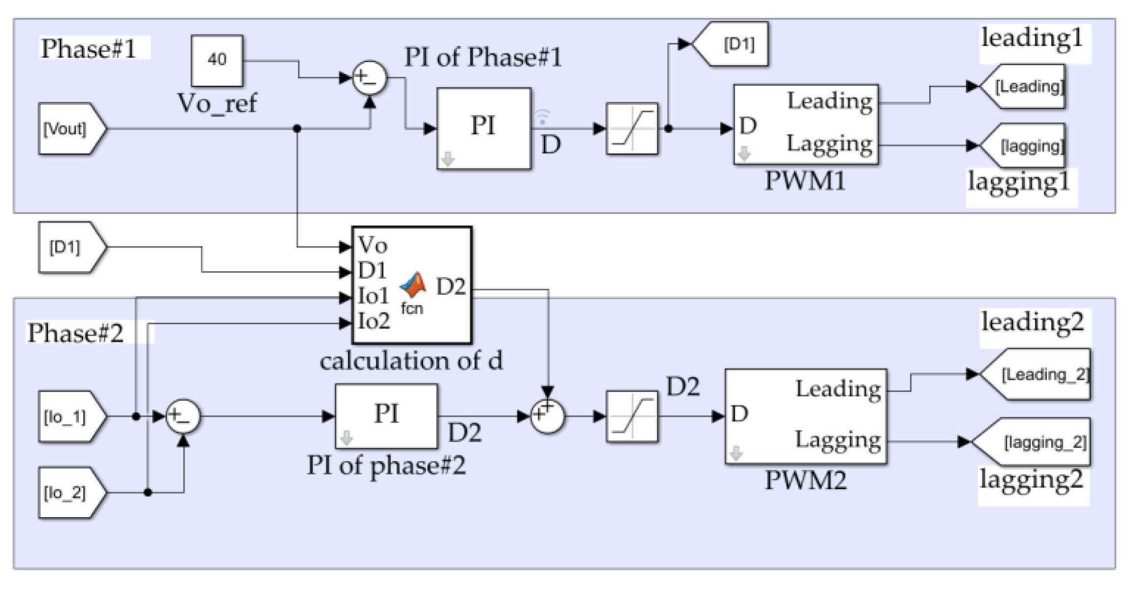
Figure 11.
Block diagram of parallel PSFB with DHC.
Figure 11.
Block diagram of parallel PSFB with DHC.
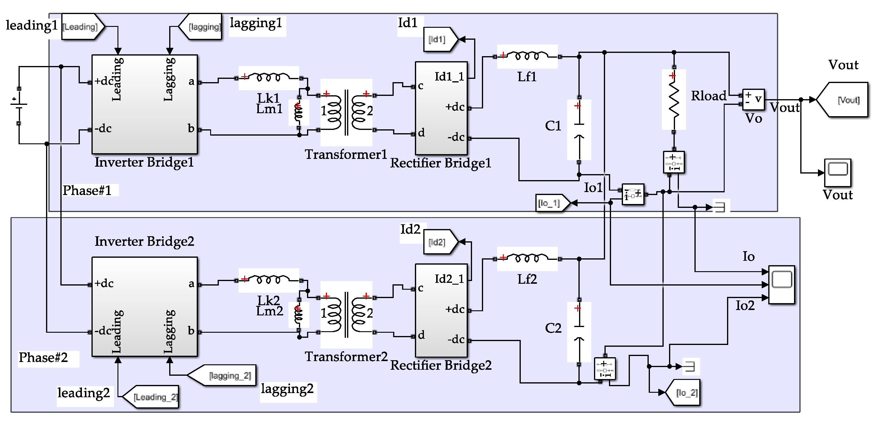
Figure 12.
Circuit part of simulation model.
Figure 12.
Circuit part of simulation model.
Figure 13.
Controller part of simulation model.
Figure 13.
Controller part of simulation model.
Figure 14.
Simulation result of output current and rectifier current in different output resistances when a = 1.2: (a) = 4 , = 400 W; (b) = 2.667 , = 600 W; (c) = 2 , = 800 W.
Figure 14.
Simulation result of output current and rectifier current in different output resistances when a = 1.2: (a) = 4 , = 400 W; (b) = 2.667 , = 600 W; (c) = 2 , = 800 W.
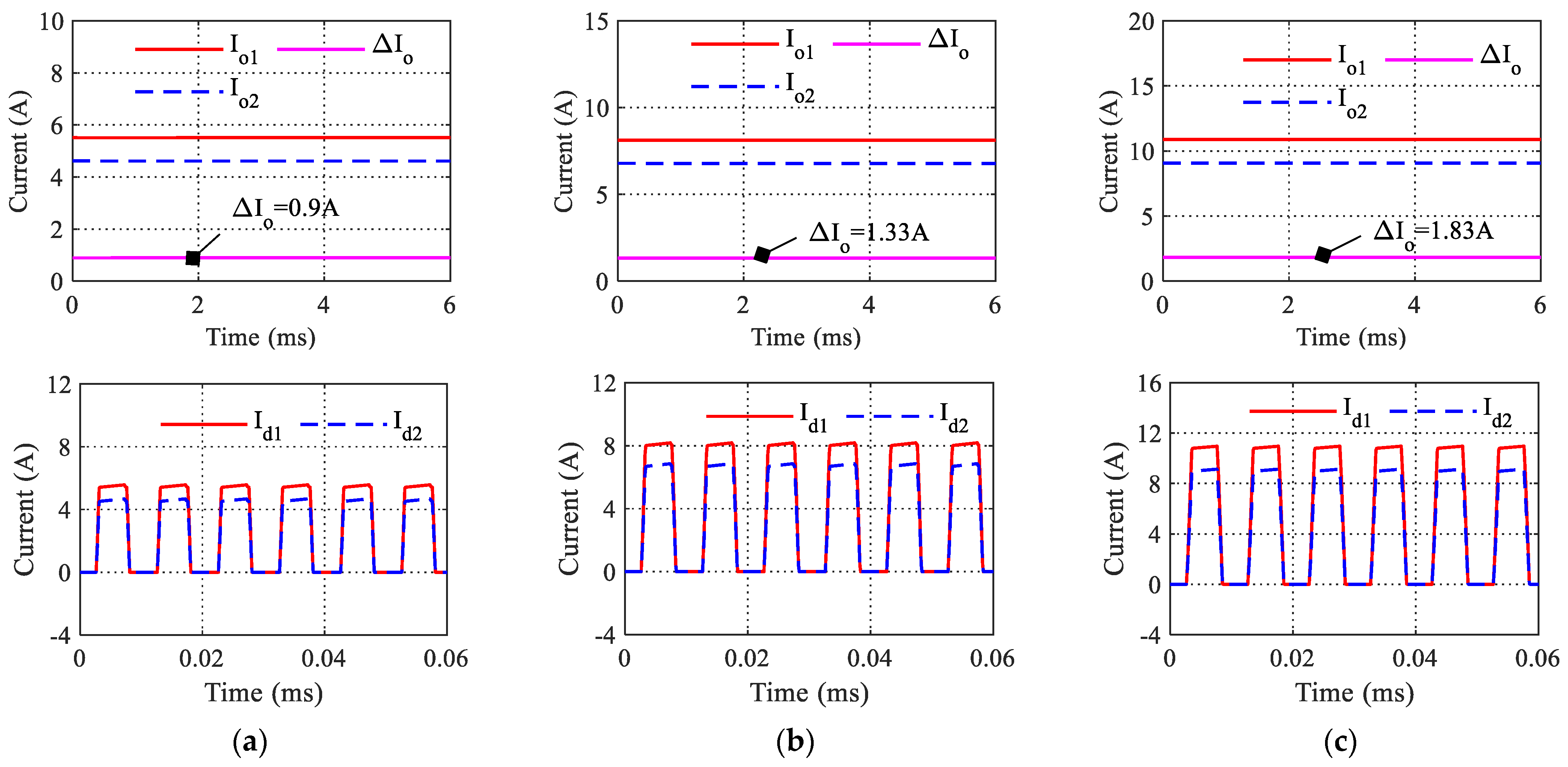
Figure 15.
Simulation result of and in different after using calculation result when a = 1.2: (a) = 4 , = 400 W; (b) = 2.667 , = 600 W; (c) = 2 , = 800 W.
Figure 15.
Simulation result of and in different after using calculation result when a = 1.2: (a) = 4 , = 400 W; (b) = 2.667 , = 600 W; (c) = 2 , = 800 W.
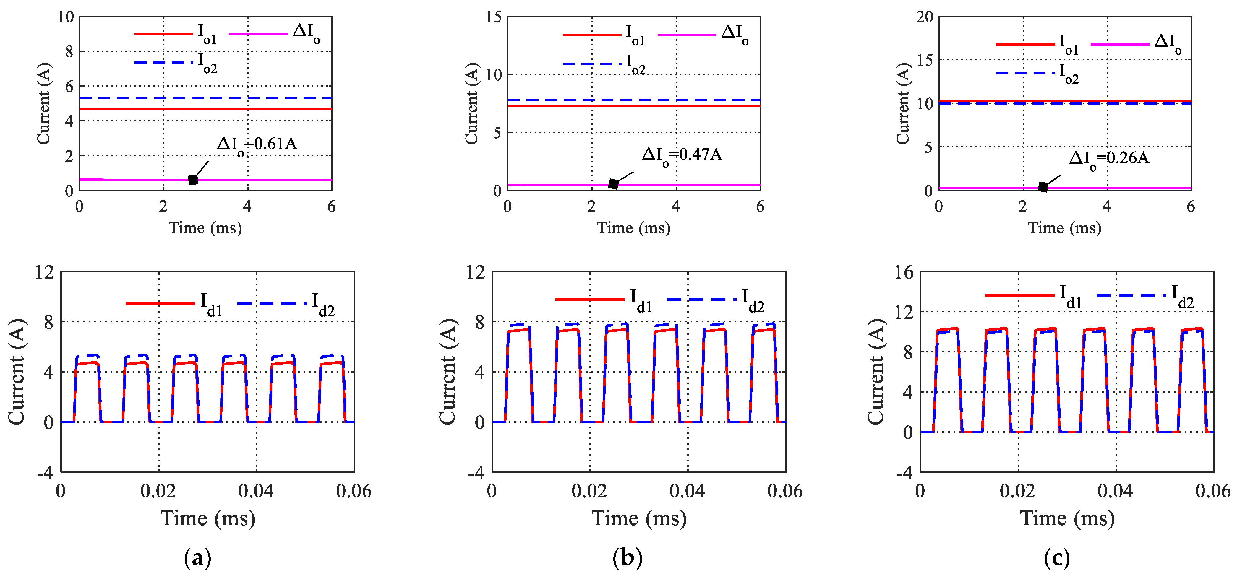
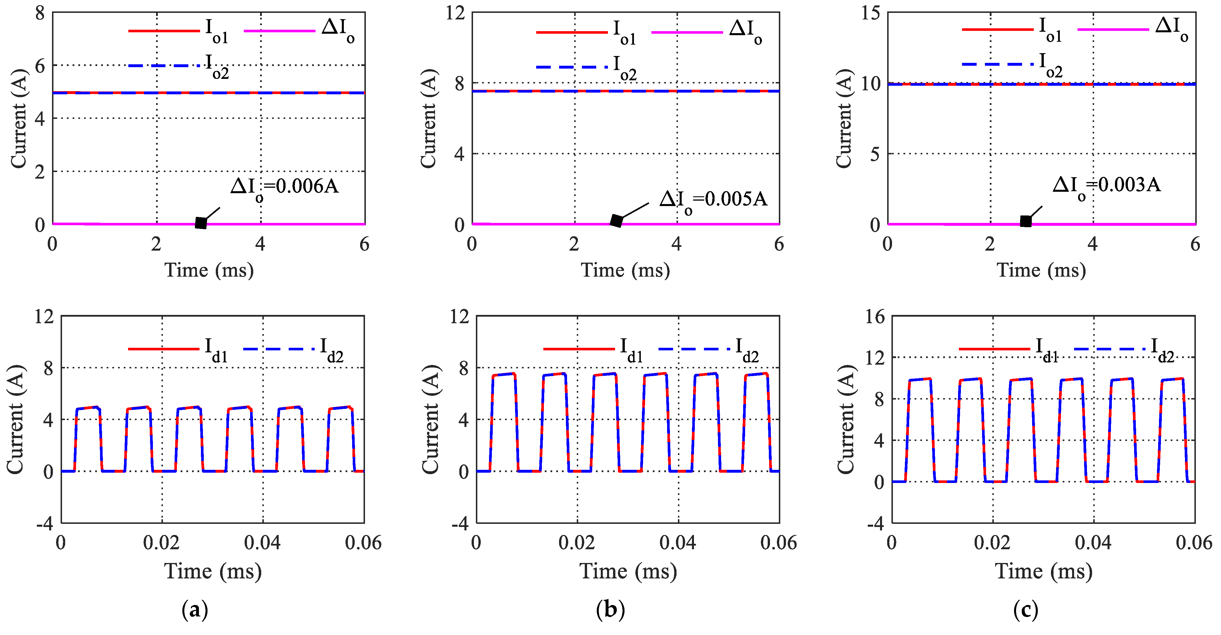
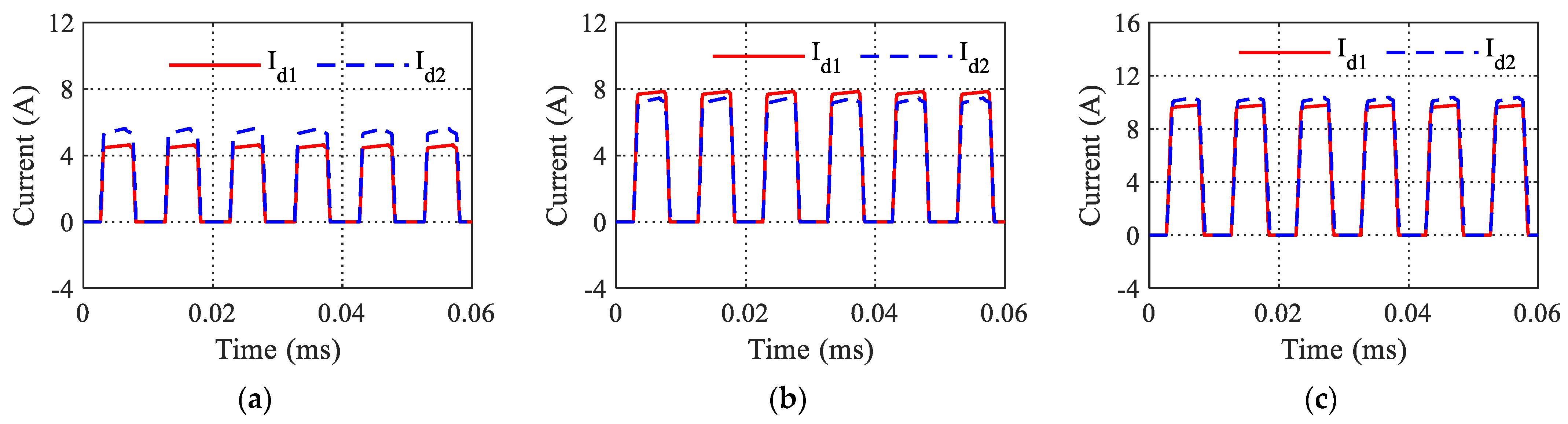
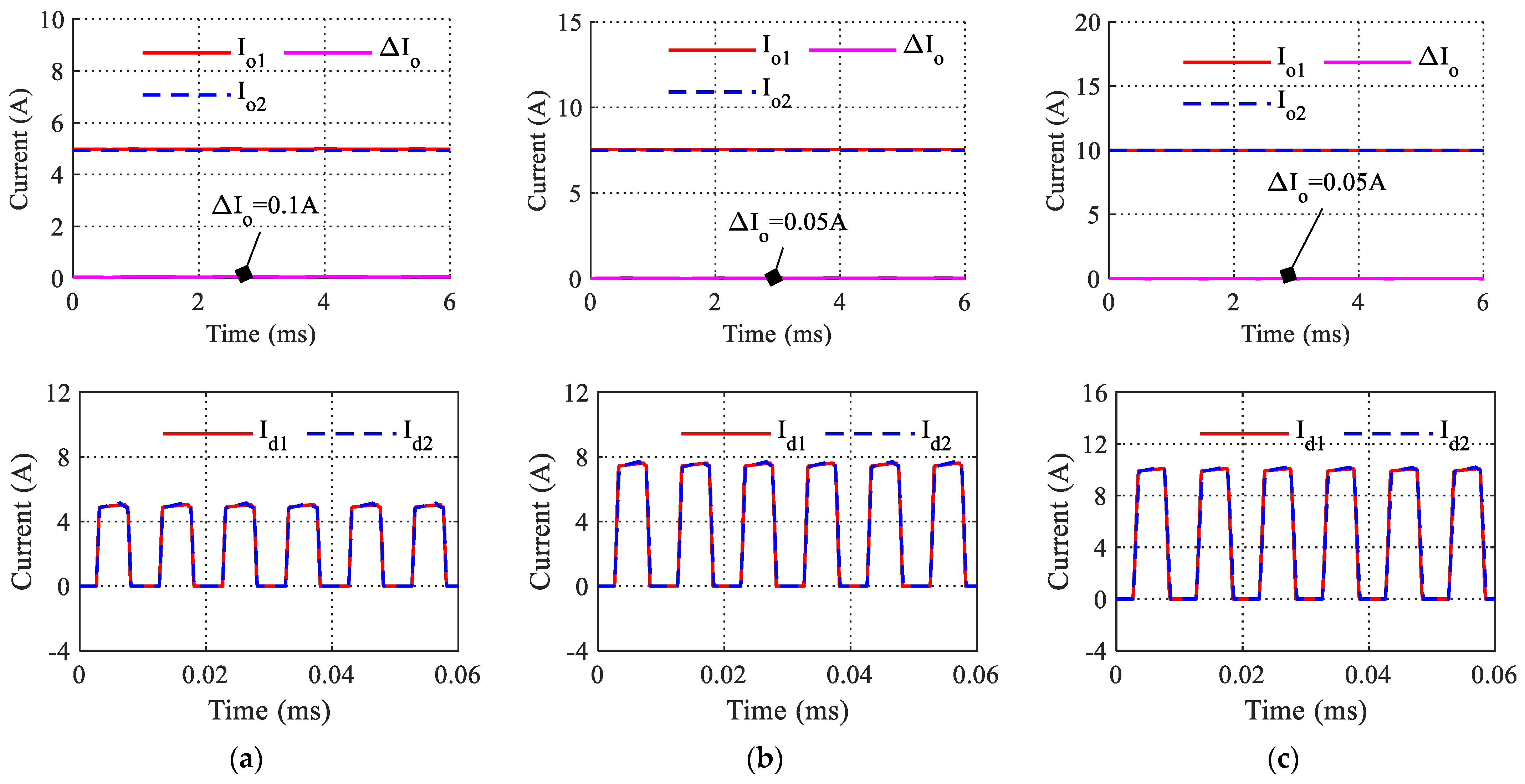
Figure 16.
Simulation result of and in different after using DHC when a = 1.2; (a) = 4 , = 400 W; (b) = 2.667 , = 600 W; (c) = 2 , = 800 W.
Figure 16.
Simulation result of and in different after using DHC when a = 1.2; (a) = 4 , = 400 W; (b) = 2.667 , = 600 W; (c) = 2 , = 800 W.
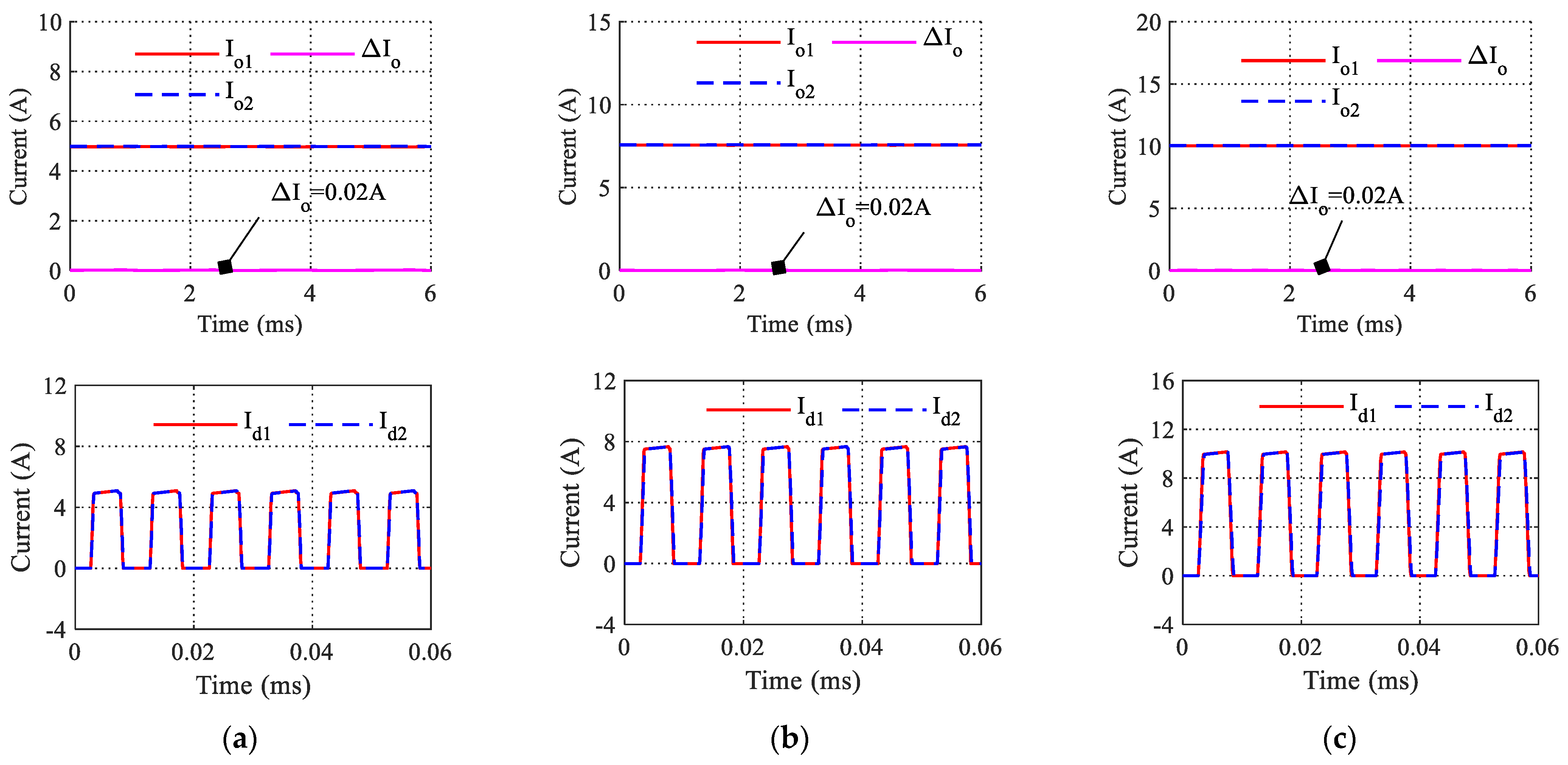
Figure 17.
Simulation result of and in different when b = 1.2: (a) = 4 , = 400 W; (b) = 2.667 , = 600 W; (c) = 2 , = 800 W.
Figure 17.
Simulation result of and in different when b = 1.2: (a) = 4 , = 400 W; (b) = 2.667 , = 600 W; (c) = 2 , = 800 W.
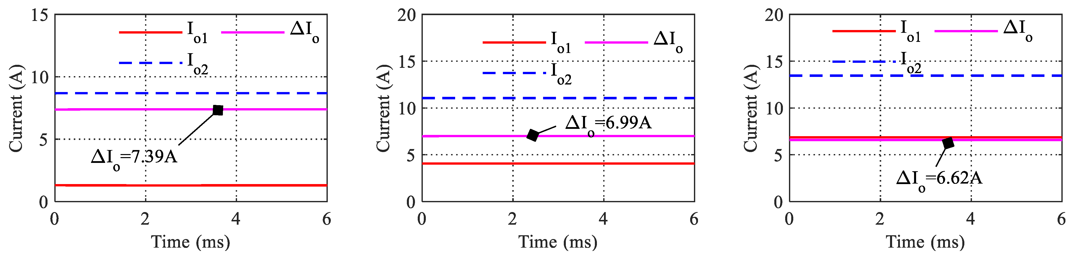
Figure 18.
Simulation result of and in different without current sharing control when c = 1.2: (a) = 4 , = 400 W; (b) = 2.667 , = 600 W; (c) = 2 , = 800 W.
Figure 18.
Simulation result of and in different without current sharing control when c = 1.2: (a) = 4 , = 400 W; (b) = 2.667 , = 600 W; (c) = 2 , = 800 W.
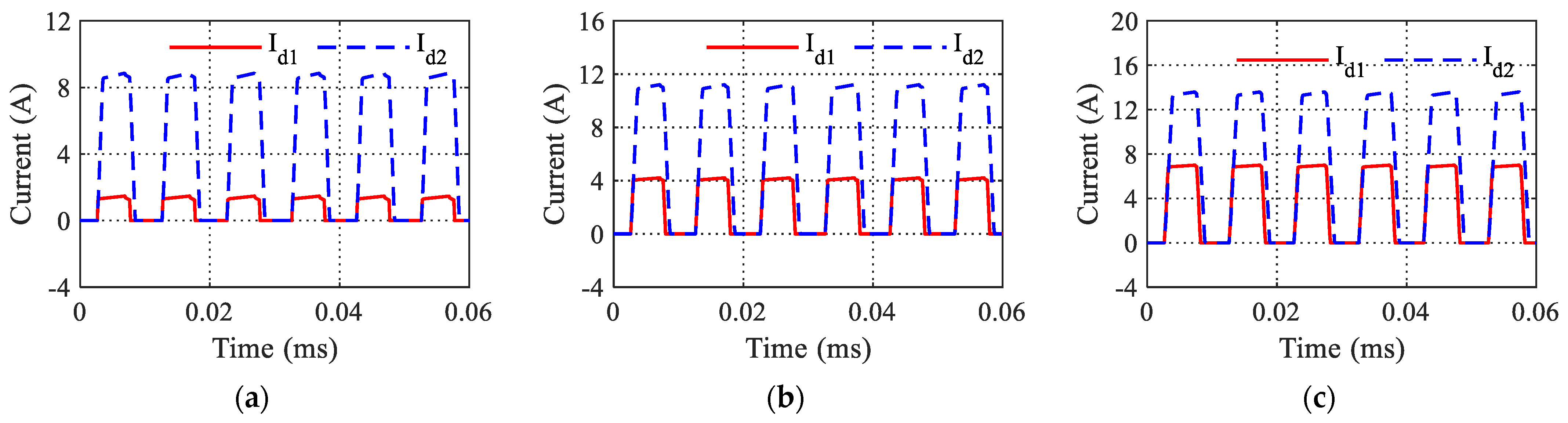
Figure 19.
Simulation result of and in different after only using calculation result when c = 1.2: (a) = 4, = 400 W; (b) = 2.667 , = 600 W; (c) = 2 , = 800 W.
Figure 19.
Simulation result of and in different after only using calculation result when c = 1.2: (a) = 4, = 400 W; (b) = 2.667 , = 600 W; (c) = 2 , = 800 W.
Figure 20.
Simulation result of and in different after using DHC when c = 1.2: (a) = 4 , = 400 W; (b) = 2.667 , = 600 W; (c) = 2 , = 800 W.
Figure 20.
Simulation result of and in different after using DHC when c = 1.2: (a) = 4 , = 400 W; (b) = 2.667 , = 600 W; (c) = 2 , = 800 W.
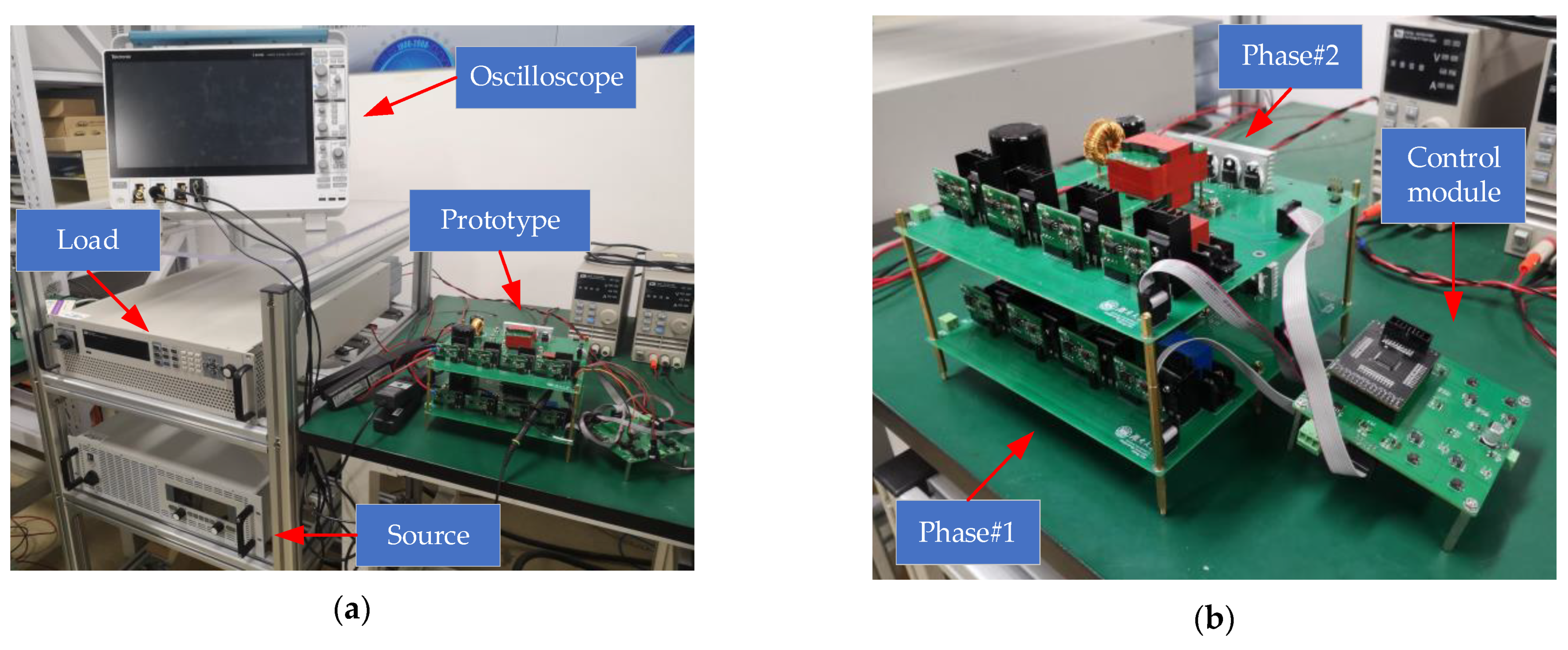
Figure 21.
Testing bench and prototype of two-phase PSFB converter: (a) testing bench; (b) prototype.
Figure 21.
Testing bench and prototype of two-phase PSFB converter: (a) testing bench; (b) prototype.
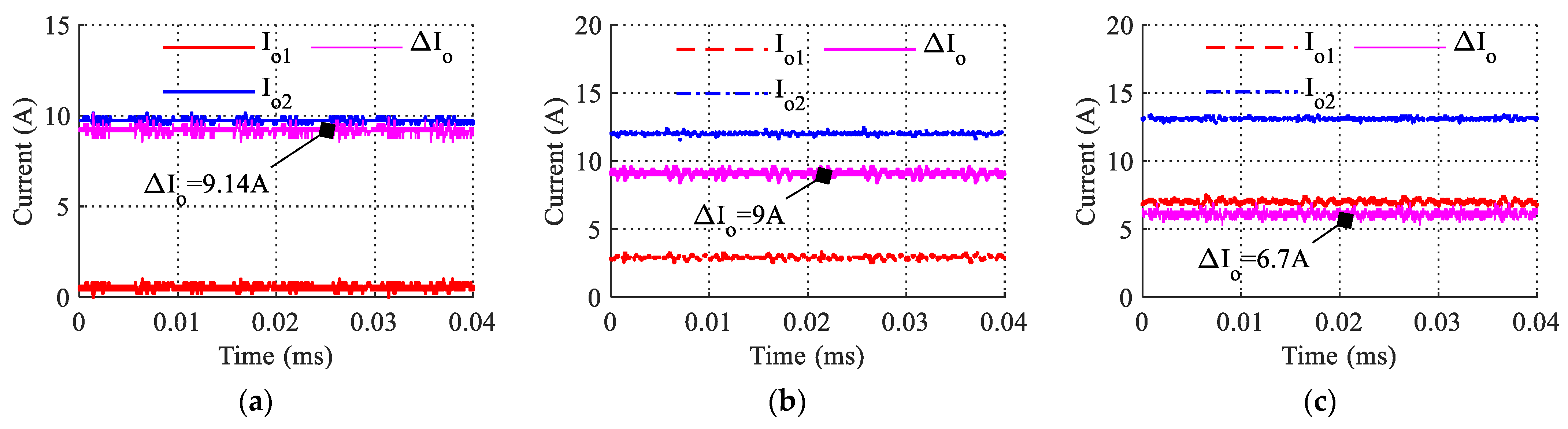
Figure 22.
Experimental result of output current without current sharing control in different : (a) = 4 , = 400 W; (b) = 2.667 , = 600 W; (c) = 2 , = 800 W.
Figure 22.
Experimental result of output current without current sharing control in different : (a) = 4 , = 400 W; (b) = 2.667 , = 600 W; (c) = 2 , = 800 W.
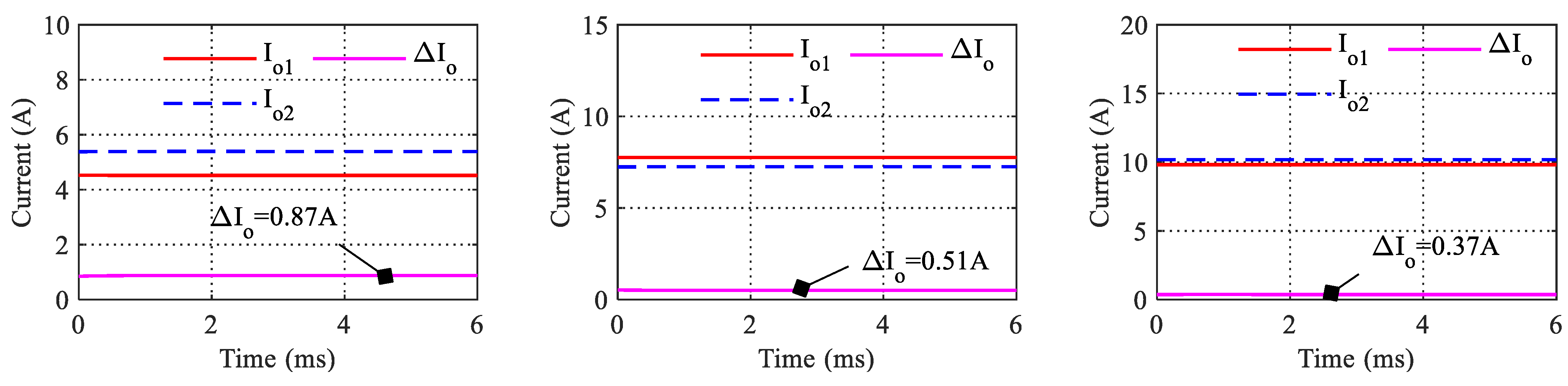
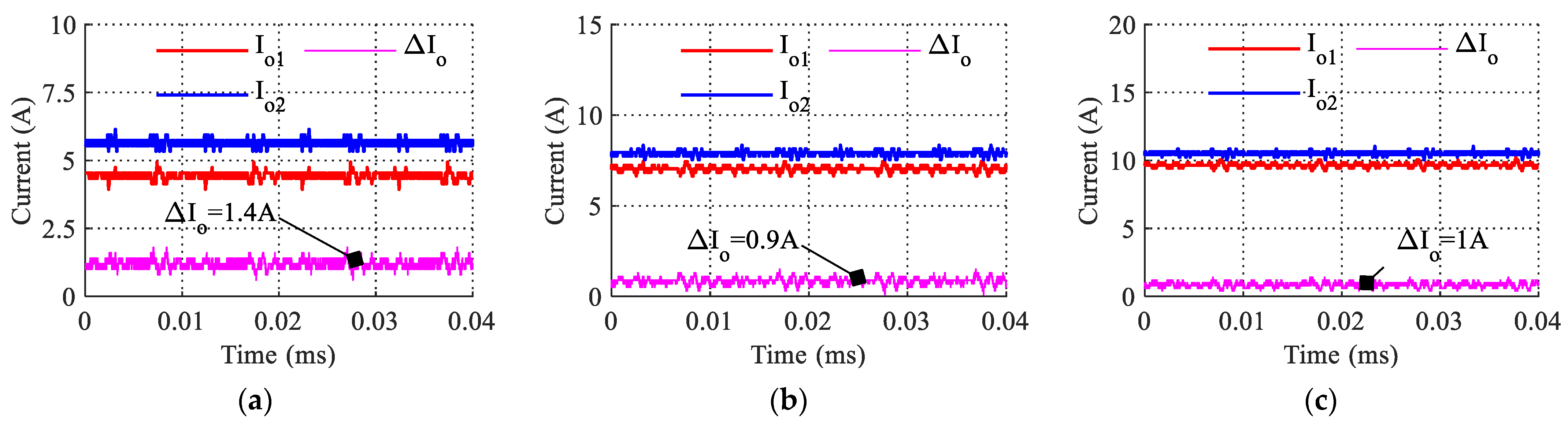
Figure 23.
Experimental result of output current after only using calculation compensation: (a) = 4 , = 400 W; (b) = 2.667 , = 600 W; (c) = 2 , = 800 W.
Figure 23.
Experimental result of output current after only using calculation compensation: (a) = 4 , = 400 W; (b) = 2.667 , = 600 W; (c) = 2 , = 800 W.
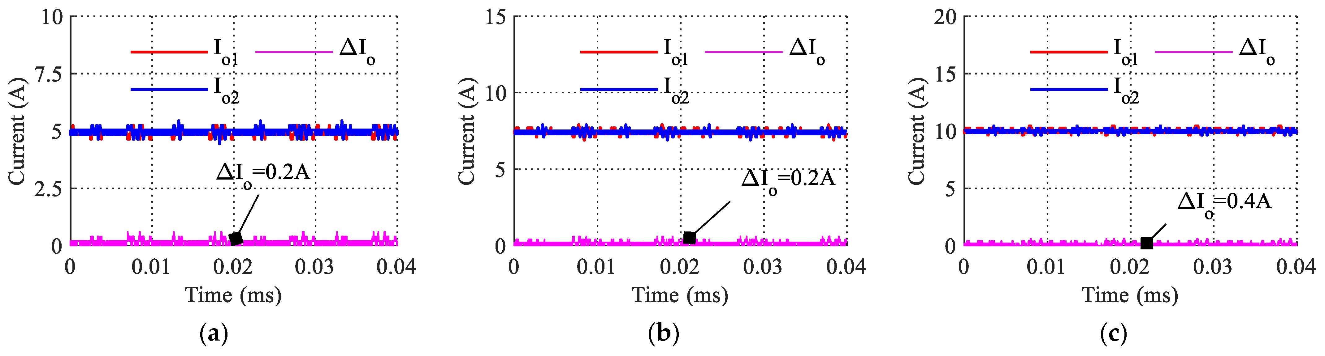
Figure 24.
Experimental result of output current after using DHC: (a) = 4 , = 400 W; (b) = 2.667 , = 600 W; (c) = 2 , = 800 W.
Figure 24.
Experimental result of output current after using DHC: (a) = 4 , = 400 W; (b) = 2.667 , = 600 W; (c) = 2 , = 800 W.
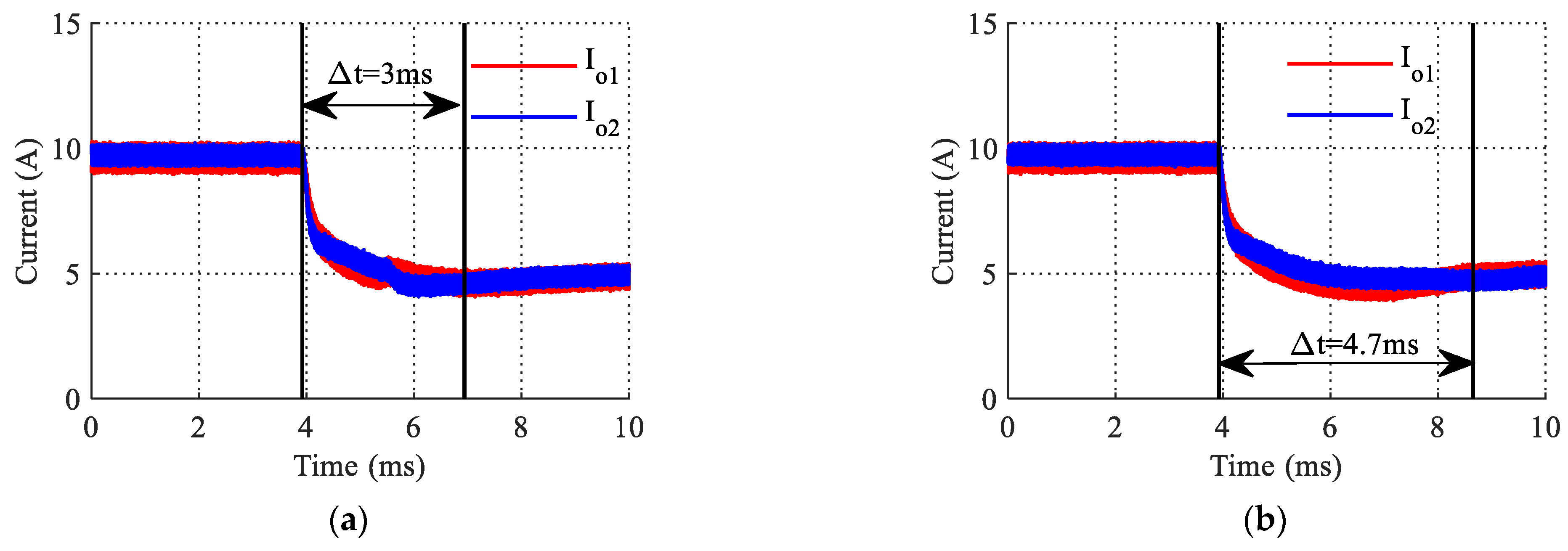
Figure 25.
Experimental output current waveforms under 800 W–400 W load transient: (a) DHC control; (b) conventional PI control.
Figure 25.
Experimental output current waveforms under 800 W–400 W load transient: (a) DHC control; (b) conventional PI control.
Table 1.
Characteristics of different connection types.
Table 1.
Characteristics of different connection types.
| Connection Type | Application
Situation | Input Side
Characteristics | Output Side
Characteristics |
|---|
| ISOS | High input and output voltage | voltage imbalance and current equalization | voltage imbalance and current equalization |
| ISOP | Converting from high voltage to low voltage | voltage imbalance and current equalization | voltage equalization and current imbalance |
| IPOS | Converting from low voltage to high voltage | voltage equalization and current imbalance | voltage imbalance and current equalization |
| IPOP | Power expansion | voltage equalization and current imbalance | voltage equalization and current imbalance |
Table 2.
Values of PSFB-related parameters.
Table 2.
Values of PSFB-related parameters.
| Parameter | Value |
|---|
| Rated input voltage | 200 V |
| Leakage inductor | 30 |
| Filter inductor | 200 |
| Transformer ratio | 24:6 |
| Rated output voltage | 40 V |
| Total output power | half 400 W, total 800 W |
| Switch frequency | 100 kHz |
Table 3.
Data comparison of different output power when a = 1.2.
Table 3.
Data comparison of different output power when a = 1.2.
| | | | | |
|---|
| 400 W | 10.12 A | = 5.5 A | = 0.9 A | = 0.543 | 8.89% |
| = 4.61 A | = 0.456 |
| 600 W | 14.89 A | = 8.11 A | = 1.33 A | = 0.545 | 8.93% |
| = 6.78 A | = 0.455 |
| 800 W | 19.96 A | = 10.89 A | = 1.83 A | = 0.546 | 9.17% |
| = 9.1 A | = 0.456 |
Table 4.
Data comparison of different output power after only using calculation result when a = 1.2.
Table 4.
Data comparison of different output power after only using calculation result when a = 1.2.
| | | | | |
|---|
| 400 W | 9.97 A | = 4.68 A | = 0.61 A | = 0.47 | 6.07% |
| = 5.29 A | = 0.53 |
| 600 W | 15.08 A | = 7.3 A | = 0.47 A | = 0.484 | 3.12% |
| = 7.78 A | = 0.516 |
| 800 W | 20.23 A | = 10.24 A | = 0.26 A | = 0.506 | 1.28% |
| = 9.99 A | = 0.494 |
Table 5.
Data comparison of different output power after using DHC when a = 1.2.
Table 5.
Data comparison of different output power after using DHC when a = 1.2.
| | | | | |
|---|
| 400 W | 9.97 A | = 4.98 A | = 0.02 A | = 0.5 | 0.2% |
| = 4.99 A | = 0.5 |
| 600 W | 15.14 A | = 7.57 A | = 0.02 A | = 0.5 | 0.13% |
| = 7.56 A | = 0.5 |
| 800 W | 20.07 A | = 10.04 A | = 0.02 A | = 0.5 | 0.1% |
| = 10.03 A | = 0.5 |
Table 6.
Data comparison of different output power when b = 1.2.
Table 6.
Data comparison of different output power when b = 1.2.
| | | | | |
|---|
| 400 W | 9.92 A | = 4.96 A | = 0.006 A | = 0.5 | 0.06% |
| = 4.96 A | = 0.5 |
| 600 W | 15.06 A | = 7.53 A | = 0.005 A | = 0.5 | 0.03% |
| = 7.53 A | = 0.5 |
| 800 W | 19.8 A | = 9.89 A | = 0.003 A | = 0.5 | 0.02% |
| = 9.91 A | = 0.5 |
Table 7.
Data comparison of different output power without current sharing control when c = 1.2.
Table 7.
Data comparison of different output power without current sharing control when c = 1.2.
| | | | | |
|---|
| 400 W | 10 A | = 1.3 A | = 7.39 A | = 0.13 | 73.98% |
| = 8.69 A | = 0.87 |
| 600 W | 15.11 A | = 4.06 A | = 6.99 A | = 0.269 | 46.26% |
| = 11.05 A | = 0.731 |
| 800 W | 20.3 A | = 6.84 A | = 6.62 A | = 0.337 | 32.61% |
| = 13.46 A | = 0.663 |
Table 8.
Data comparison of different output power after only using calculation result when c = 1.2.
Table 8.
Data comparison of different output power after only using calculation result when c = 1.2.
| | | | | |
|---|
| 400 W | 9.91 A | = 4.52 A | = 0.87 A | = 0.456 | 8.82% |
| = 5.39 A | = 0.544 |
| 600 W | 15.01 A | = 7.76 A | = 0.51 A | = 0.517 | 3.41% |
| = 7.25 A | = 0.483 |
| 800 W | 20.01 A | = 9.82 A | = 0.37 A | = 0.491 | 1.84% |
| = 10.19 A | = 0.509 |
Table 9.
Data comparison of different output power after using DHC when c = 1.2.
Table 9.
Data comparison of different output power after using DHC when c = 1.2.
| | | | | |
|---|
| 400 W | 9.92 A | = 4.91 A | = 0.1 A | = 0.495 | 1.01% |
| = 5.01 A | = 0.505 |
| 600 W | 15.04 A | = 7.51 A | = 0.05 A | = 0.499 | 0.33% |
| = 7.52 A | = 0.5 |
| 800 W | 20 A | = 10.02 A | = 0.05 A | = 0.501 | 0.25% |
| = 9.98 A | = 0.499 |
Table 10.
Prototype circuit component values.
Table 10.
Prototype circuit component values.
| Parameter | Value |
|---|
| Rated input voltage | 200 V |
| Rated output voltage | 40 V |
| Full load current | 10 A × 2 |
| Rated output power | 400 W × 2 |
| Leakage inductor | 31.29 (phase#1), 27.59 (phase#2) |
| Filter inductor | 237.69 (phase#1), 265.86 (phase#2) |
| Transformer ratio | 24:6(phase#1), 24:7(phase#2) |
| Switch frequency | 100 kHz |
Table 11.
Experimental data without current sharing control in different output power.
Table 11.
Experimental data without current sharing control in different output power.
| | | | | |
|---|
| 400 W | 10.34 A | = 0.6 A | = 9.14 A | = 0.058 | 88.39% |
| = 9.74 A | = 0.942 |
| 600 W | 14.88 A | = 2.94 A | = 9 A | = 0.198 | 60.48% |
| = 11.94 A | = 0.802 |
| 800 W | 20.5 A | = 6.9 A | = 6.7 A | = 0.337 | 32.68% |
| = 13.6 A | = 0.663 |
Table 12.
Experimental data after only using calculation compensation.
Table 12.
Experimental data after only using calculation compensation.
| | | | | |
|---|
| 400 W | 10.08 A | = 4.34 A | = 1.4 A | = 0.431 | 13.9% |
| = 5.74 A | = 0.569 |
| 600 W | 14.98 A | = 7.04 A | = 0.9 A | = 0.47 | 6.01% |
| = 7.94 A | = 0.53 |
| 800 W | 20.28 A | = 9.64 A | = 1 A | = 0.475 | 4.93% |
| = 10.64 A | = 0.525 |
Table 13.
Experimental data after using DHC.
Table 13.
Experimental data after using DHC.
| | | | | |
|---|
| 400 W | 10.08 A | = 4.94 A | = 0.2 A | = 0.49 | 1.98% |
| = 5.14 A | = 0.501 |
| 600 W | 15 A | = 7.4 A | = 0.2 A | = 0.493 | 1.33% |
| = 7.6 A | = 0.507 |
| 800 W | 20.08 A | = 9.84 A | = 0.4 A | = 0.49 | 1.99% |
| = 10.24 A | = 0.51 |


 ,
, 


