1. Introduction
Wide-bandgap oxide semiconductors have gained considerable attention and received great interest due to their potential for applications in optoelectronic devices, photovoltaic devices, and transparent oxide electronics, such as ultraviolet photodetectors, short wavelength light-emitting diodes, thin-film solar cells, transparent resistive random access memory, and transparent field-effect transistors [
1,
2,
3,
4]. The fabrication of light-emitting diodes, p-n junction photodetectors, and complementary metal-oxide-semiconductor devices requires the combination of both n-type and p-type oxide semiconductors. The lack of availability of stable p-type oxide semiconductors limits the electrical efficiency of p-n junction-based devices or bipolar device applications [
3,
5]. Therefore, the development of stable and reproducible p-type oxide semiconductor thin films is necessary.
The crystalline wurtzite ZnO exhibits n-type conductivity due to a deviation from chemical stoichiometry and the presence of native point defects such as O vacancies (Vo) and Zn interstitials (Zn
i) that makes the electrons easily be excited to the conduction band [
2,
6]. The difficulty in achieving p-type ZnO semiconductors is caused by a combination of deep acceptor levels, the low solubility of acceptors, and a strong self-compensation effect [
7,
8]. Previous studies demonstrated that the impurity doping of ZnO is an important approach for modulating the carrier concentration and electrical resistivity to satisfy device applications [
9,
10]. A sufficient amount of acceptors should be generated to overcome the n-type back ground, such as any donor-like defects created through preparation processes. It has been suggested that the group V element nitrogen (N) may be a potential acceptor dopant for O site substitution in ZnO to obtain p-type conductivity, for N has the smallest ionization energy among the group V dopants (N, P, and As) [
2,
11]. In addition, N (0.146 nm) and O (0.140 nm) have close ionic radii, and so N ions may easily be substituted on O sites of the ZnO lattice [
12]. Moreover, the N–O bond length (1.88 Å) is close to the Zn–O bond length (1.93 Å) [
13]. Kim’s group reported that the incorporation of N as a dopant changed the conductivity of sol-gel-derived ZnO thin films from n-type to p-type and produced ZnO:N thin films with a hole concentration of 8.11 × 10
16 cm
−3 when the N doping content reached 20 at.% in the resultant solution [
14]. However, the production of device-quality p-type conduction in N-doped ZnO thin films remains a challenge due to the low dopant solubility in the host material and high ionization energy [
11].
Co-doping of two kinds of extrinsic atoms (using acceptors and donors simultaneously) is considered an effective method for producing stable p-type conductivity in ZnO semiconductor thin films [
7,
15,
16]. Previous experimental studies found that acceptor and donor co-doped ZnO thin films not only exhibited p-type conductivity but also showed reasonable stability and reproducibility in electrical characteristics [
17,
18,
19]. It was reported that simultaneous doping of nitrogen and group III elements can improve the hole concentration and enhance the stability of p-type ZnO thin film because the doping of the reactive donor element increases the solubility of nitrogen in ZnO [
20,
21,
22,
23]. According to first-principles calculations, Yan et al. proposed that the formation of passive acceptor-donor (Ga–N) complexes can create an impurity band above the valence-band maximum (VBM) in ZnO crystal based on reduction of the ionization energies of dopants [
8]. A theoretical study by Duan et al. reported that the ionization energy of Ga–2N complex is lower than that of the single N acceptor [
11]. The generation of N–Ga–N complexes could increase the solubility percentage of N ionized dopants and achieve shallower acceptor levels [
6]. A previous report noted that the co-doping of Ga and N in ZnO thin films achieved the best p-type character among the types of impurity co-doped ZnO thin films [
8]. Theoretical calculations also predict that Ga–N co-doped ZnO would yield better p-type conduction than Al–N co-doped ZnO [
11]. This prediction is consistent with numerous experimental finding.
Several thin film deposition techniques have been employed to produce the group III (B, Al, Ga, and In)–N co-doped p-type ZnO semiconductor thin films including chemical vapor deposition, molecular-beam epitaxy, pulsed laser deposition, radio-frequency (rf) magnetron sputtering, spray pyrolysis, and the sol-gel method [
2,
7]. Most researchers have focused on the preparation of p-type ZnO thin films and investigated the effects of acceptor-donor co-doping on the physical properties. The authors noted that few studies have reported the electrical stability of solution-processed p-type ZnO thin films. There is no report on Ga–N co-doping p-type ZnO thin films prepared by the sol-gel method. Therefore, we prepared ZnO, ZnO:N, and ZnO:Ga–N thin films on glass substrates via the sol-gel method and spin-coating technique. The structural-physical properties relation of ZnO-based semiconductor thin films was investigated in detail through variation of the structural features to examine if they affect the optical properties and electrical characteristics. In addition, the electrical stability of p-type ZnO-based thin films was verified and is reported in this study.
3. Results and Discussion
Various types of nitrogen (N) sources, including NH
3, N
2, NO, N
2O, and CH
3COONH
4 have been successfully used to prepare of device-quality p-type ZnO semiconductor thin films. In this study, the N dopant was obtained through decomposition of ammonium acetate to acetamide and then to CO, NO, and NO
2 [
24]. The NO and NO
2 acted as the N sources. It was suggested that NO easily forms N
O acceptors, which are shallow acceptors in ZnO [
2,
8]. Moreover, it was necessary to provide oxygen to suppress oxygen vacancy (Vo) formation during the preparation of solution-processed p-type ZnO thin films. Because Vo may form as a compensation center in p-type ZnO [
25], we performed the post deposition crystallization heat treatment in pure oxygen atmosphere to decrease the background carrier concentration.
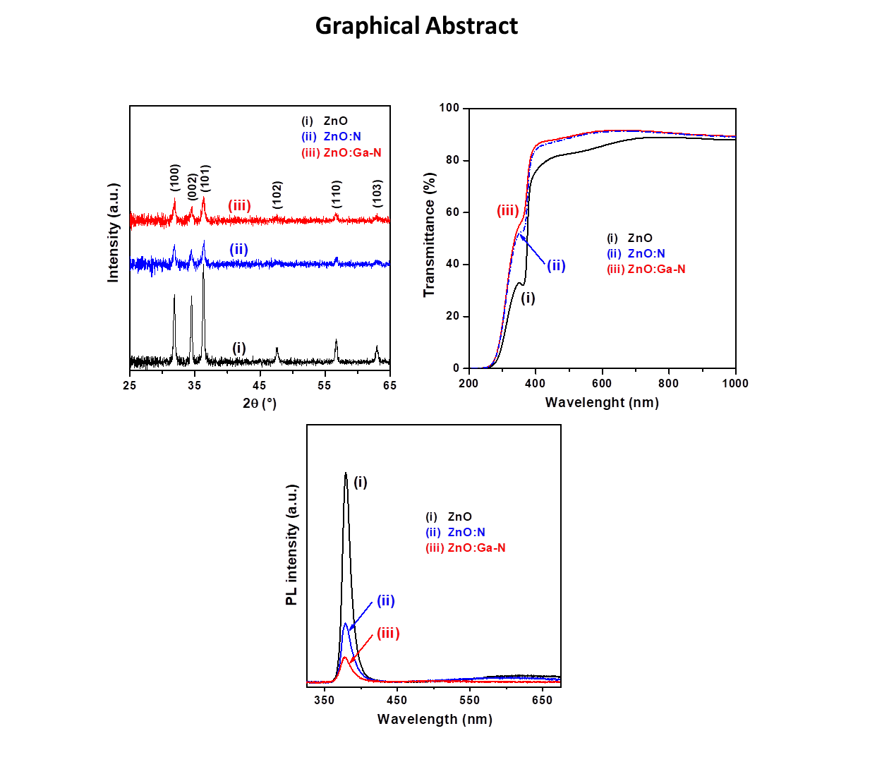
The results of the XRD examination, shown in
Figure 1, indicate that the three kinds of ZnO-based thin films were polycrystalline in nature. The intense sharp diffraction peaks suggested that the pure ZnO thin film had better crystallinity (pattern (i) in
Figure 1) than those of the two impurity-doped ZnO thin films. Previous studies reported that the crystalline quality of oxide thin films would be degraded by impurity doping [
10,
26,
27]. Comparison of collected XRD patterns (in 2θ range from 25° to 65°) with the standard JCPDS file of ZnO crystal (JCPDS No. 36-1451) indicated the hexagonal wurtzite phase in the ZnO-based thin films. In addition, no X-ray diffraction signals related to other crystal phases, such as GaN, Ga
2O
3, and Zn
3N
2, were detected from the set of thin film samples, indicating the formation of a single phase.
A preferential orientation may occur due to nucleation, horizontal growth of the nuclei and vertical growth of the closed layer. As shown in
Figure 1, we not only confirmed that these as-prepared ZnO thin films had a predominance of hexagonal wurtzite phase but also observed that they achieved a favorable orientation along the (101) plane. The relative intensities of
I(101)/
I(1000) + (002) + (101) for the ZnO, ZnO:N, and ZnO:Ga–N samples were 0.422, 0.406, and 0.387, respectively. The calculated results reveal that the relative diffraction intensity of the undoped sample (0.422) was significantly smaller than that of the relative intensity (0.497) obtained from the standard JCPDS database; incorporation of N and Ga–N into the ZnO changed the growth rate of the (101) plane such that the three main diffraction planes had close growth rates. It is noted that the diffraction signals of the (102) and (103) planes were very weak for the two impurity-doped samples, implying an apparent decrease in crystallinity. According to the above discussion, we found that these sol-gel-derived ZnO-based thin films had no preferential orientation; impurity doping favored random growth of crystallites and caused degradation of the crystallinity. The average crystallite sizes of the thin film samples were quantified from the full widths at half-maximum and the Bragg diffraction angles of the three major diffraction peaks, (100), (002), and (101), with Scherrer’s formula and are presented in
Table 1.
Table 1 summarizes our examined and calculated results on the structural features and optical properties. The average crystallite sizes for the undoped, N doped and Ga–N co-doped ZnO thin films were 26.9, 20.4, and 17.0 nm, respectively. It was determined that all the obtained ZnO-based thin films consisted of nanocrystals; N doping significantly inhibited the crystal growth rate due to lattice distortion, and the Zn:Ga–N samples had the smallest average crystallite size.
Figure 2 shows the cross-sectional FE-SEM micrographs of ZnO-based thin films deposited onto glass substrates, which revealed good thickness uniformity. It can be seen that these oxide thin films possessed significantly granular microstructures, had homogeneous particle size distributions, and exhibited nano-sized pores inside the sol-gel-derived ZnO-based thin films. In addition, it was significantly observed that the mean particle size of the N-doped thin film was smaller than that of the undoped thin film, and the Ga–N co-doped thin film possessed the finest grade of particles. The microstructural features of the developed thin films, observed by FE-SEM, were consistent with the results of the XRD examination. The thickness of each thin film sample was estimated from the corresponding cross-sectional FE-SEM micrograph. The mean film thicknesses of the undoped, N-doped, and Ga–N co-doped ZnO thin films were found to be 85, 45, and 40 nm, respectively. The difference in film thickness between the three kinds of ZnO-based thin films can be ascribed to the variation in the viscosities of the coating solutions with the concentration of solute (metallic salts). The corresponding plane-view FE-SEM micrographs are shown in
Figure S1. In that figure, it is clearly shown that the free surfaces of the films were flat, with no visible pores or cracks in the observation area.
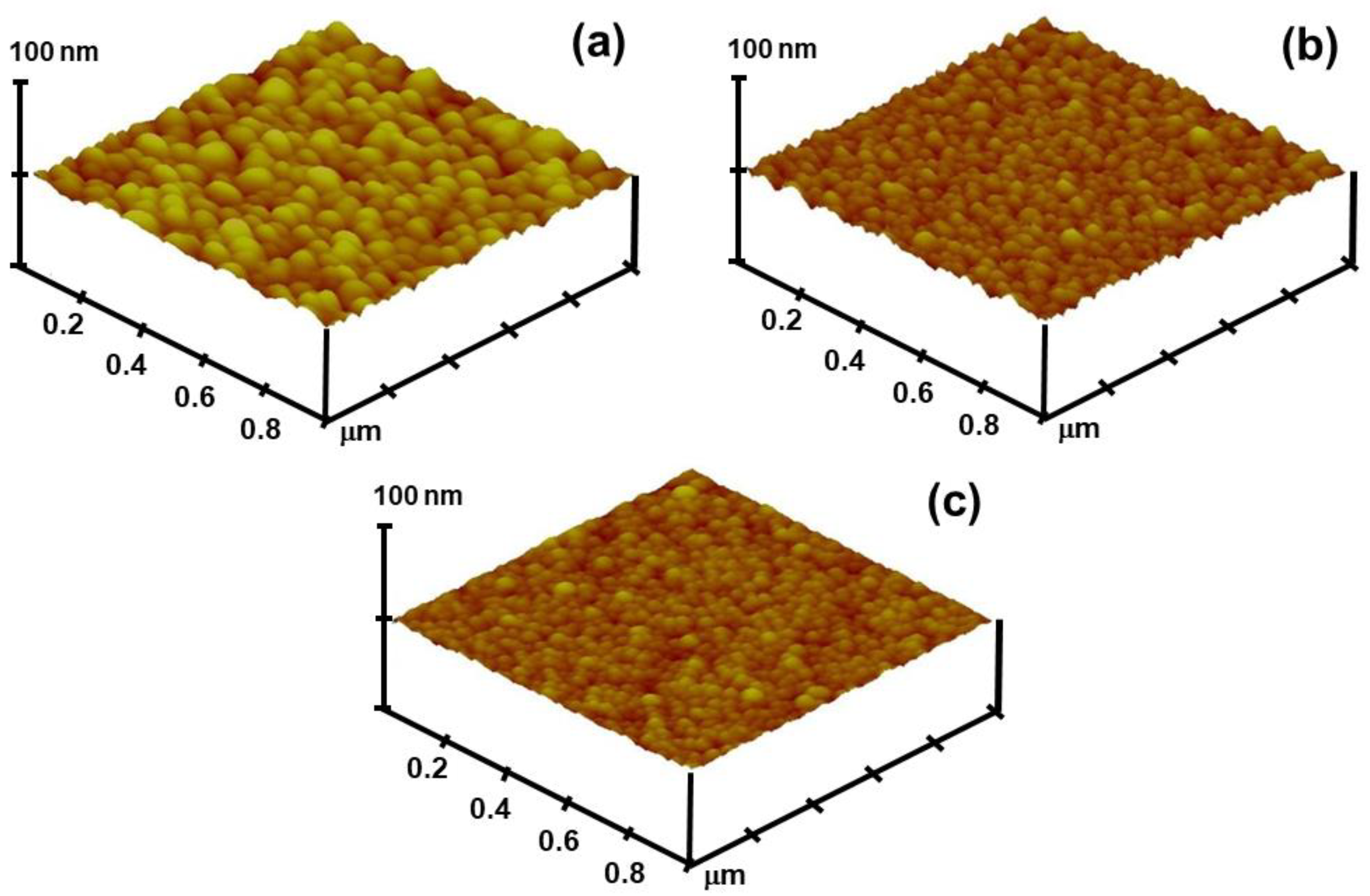
The topographic features of each thin film sample were examined by SPM to study the surface morphology and measure the root-mean-square (RMS) roughness. SPM images of the sol-gel-derived ZnO-based thin films deposited on glass substrates are presented in
Figure 3. Those images show a uniformly granular morphology and dense surface. The significant differences between the three SPM images were the particle size and surface flatness. It was observed that the co-doped sample had the smallest particles and exhibited a flat surface morphology. The average particle sizes of the ZnO, ZnO:N, and ZnO:Ga–N thin films, as estimated from the corresponding 2D SPM images (
Figure S2) in ImageJ software, were 77.3, 46.2, and 39.3 nm, respectively. The observation of surface morphological characteristics of the thin film samples by SPM had a good agreement with the XRD results.
Table 1 lists the values of RMS roughness of the ZnO, ZnO:N, and ZnO:Ga–N thin film samples, which were 3.6, 2.7, and 1.1 nm, respectively. As noted above, the impurity doping reduced the particle (crystallite) size and thereby decreased the surface roughness.
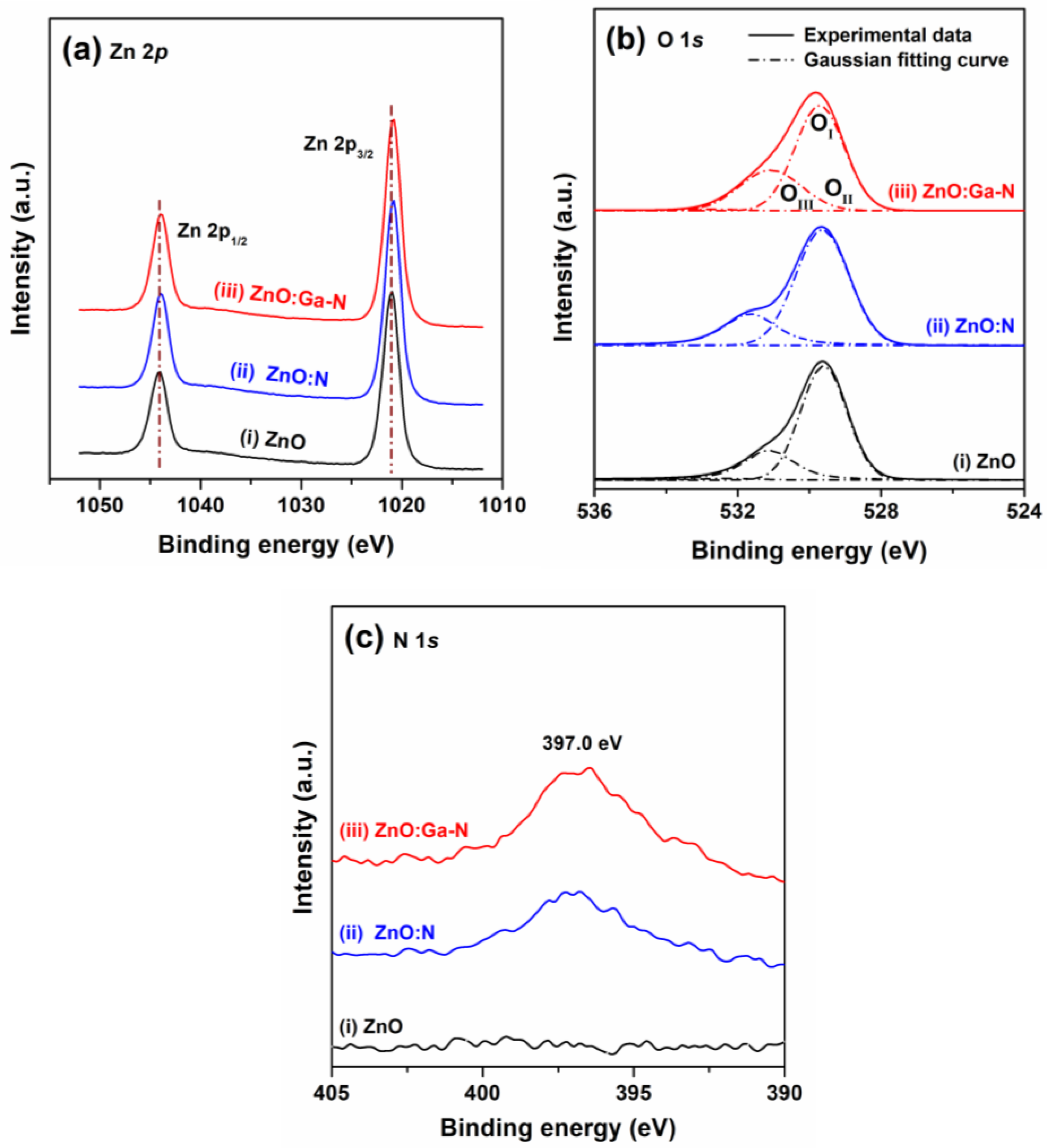
XPS examinations were performed to determine the elements responsible and identify the chemical bonding states of the ZnO-based thin films produced in this study. The narrow scan XPS spectra of Zn, O, and N regions of ZnO-based thin films are presented in
Figure 4. The core level peaks of Zn 2
p are presented in
Figure 4a; they revealed similar XPS spectra for the three samples. The peaks of binding energies at 1021.0 and 1044.2 eV for the ZnO sample corresponded to the Zn 2
p3/2 and Zn 2
p1/2 components, respectively (spectrum (i) in
Figure 4a). The electronic state of Zn 2
p3/2 is associated with the Zn
2+ ions in the ZnO lattice [
7,
28]. In addition, the Zn 2
p XPS spectra of the two impurity-doped samples showed slight shifts toward the lower binding region due to changes in the strength of the metal–oxygen bond energy because of the incorporation of N and Ga–N dopants into the ZnO nanocrystals.
As shown in
Figure 4b, the recorded O 1
s spectra were obviously broad and asymmetric on the high binding energy side (solid lines). Each O 1
s spectrum was deconvoluted to three distinct sub-curves (dashed lines) by Gaussian curve fitting and denoted with O
I, O
II, and O
III for representing three types of oxygen levels in oxide thin film samples [
29,
30]. The low binding energy component (O
I) exhibited the strongest intensity, was centered at 529.6 eV, and was associated with O
2− ions bonded with metal ions (Zn
2+ and/or Ga
3+), such as Zn–O bonds, in the ZnO lattice. The component at the middle binding energy (O
II) was centered at 531.1 eV, usually associated with the loosely bound oxygen, and related to the oxygen vacancy concentration. The component at the high binding energy region (O
III), with a weak signal, was ascribed to chemisorbed or dissociated oxygen species, such as hydroxyl groups (–OH) bonded to the surfaces and/or the grain boundaries of the polycrystalline oxide films. The calculated O
II/O
total intensity ratios for the ZnO, ZnO:N, and ZnO:Ga–N nanostructured thin films were 20.44%, 21.30%, and 27.46%, respectively. Such intensity ratios are suggested for evaluating the relative concentrations of oxygen vacancies between the oxide thin film samples. The calculated results reveal that the co-doped ZnO thin film had a higher O
II/O
total ratio than those of the un-doped and single-doped ZnO thin films, indicating that weaker metal–oxygen bonds formed in the former sample than in the latter samples. The reduced strength in the metal–oxygen bonds can be attributed to the Ga doping in ZnO:N crystals, which in turn led to a significant increase in the oxygen vacancy concentration in the ZnO:Ga–N thin film.
Figure 4c shows the N 1
s XPS core level spectra and the single peak centered at about 397.0 eV, which was related to the formation of the No–Zn bond [
23,
31] and indicated that N ions were incorporated into the ZnO lattices of the N doped and Ga–N co-doped thin films. It was also demonstrated that Ga–N co-doping enhanced the solubility of the acceptor dopant (N) in ZnO nanocrystals (spectrum (iii) in
Figure 4c. Ravichandran et al. suggested that the presence of N in the energy region, about 397.3 eV, is indicative of p-type conductivity [
32]. In addition, the Ga 2
p spectrum of the Ga–N co-doped sample is presented in
Figure S3. The peak spectrum located at 1117.4 eV corresponds to the electrical state of Ga 2
p3/2 and is ascribed to Ga
3+ in gallium(III) oxide [
33]. The actual contents of N and Ga + N in the ZnO:N and ZnO:Ga–N thin film samples were estimated by XPS analysis to be 0.52 at.%, and 1.1 at.% + 0.76 at.%. The examined results confirm that the N and Ga + N were successfully substituted into the ZnO nanocrystals and the solubility of desirable accept dopant (N) was enhanced through co-doping of Ga and N.
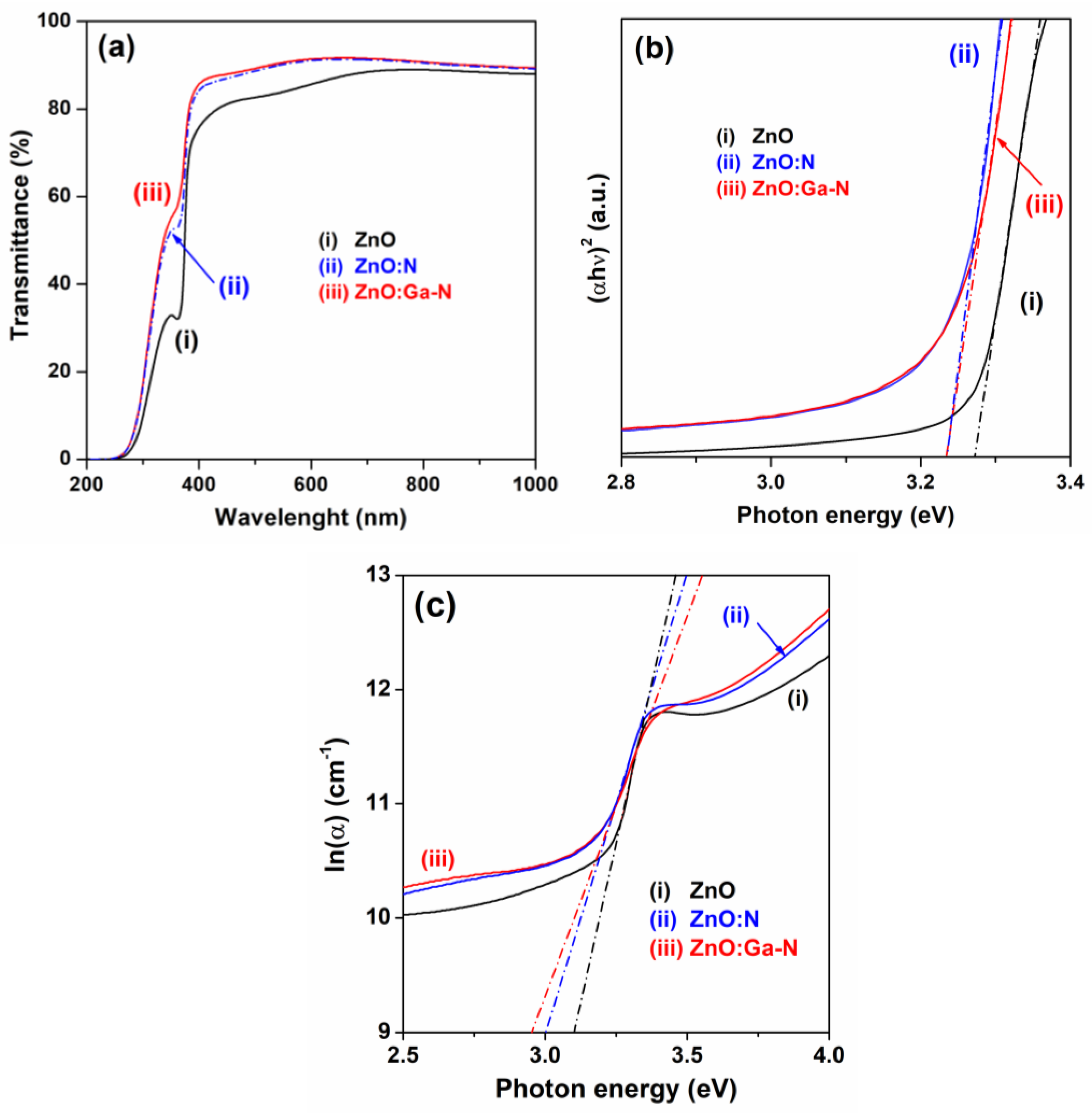
The effects on the optical characteristics of the incorporation N and Ga–N in ZnO thin films were investigated by optical transmission measurement.
Figure 5a shows three typical optical transmittance spectra, which were recorded from the samples of glass/oxide thin films in the wavelength range of 200–1000 nm. These transmittance spectra exhibited high transparency (>85.0%) in the visible region and displayed an abrupt increase in absorption in the near-UV spectral range. The character of the optical absorption edge (band-edge absorption) is related to direct optical excitation from the valence band to the conduction band and the magnitude of the bandgap energy. The slight shift toward the short wavelength region of the absorption edge in the two impurity-doped thin film samples may be associated with the finer microstructures.
The recorded optical transmittance spectra indicated that the ZnO:N and ZnO:Ga–N samples exhibited a similar transmission characteristic and had higher transparency than the ZnO sample, covering the visible light region due to the former (impurity-doped samples) being thinner and having a flatter free surface (see
Figure 2 and
Figure 3) compared with the latter (undoped sample). The average transmittances of undoped and impurity-doped ZnO thin film samples in the visible region (400 to 800 nm) were about 85.0% and approached 90.0% (the fourth column in
Table 1). It is known that the optical transmittance of functional oxide thin films is strongly affected by film thickness, surface roughness, densification, crystallinity, and structural homogeneity.
The absorption coefficient (α), one of the intrinsic optical parameters of functional oxide films, can serve as a rough estimation from measured transmittance data with the Beer–Lambert law (α = [ln(1/T)]/d
f), where d
f is the thickness of the examined thin film sample, by assuming reflectance to be negligible (
R = 0). The calculated results are listed in
Table 1. These results reveal that the average absorption coefficient of the undoped sample approached 1.9 × 10
4 cm
−1 in the visible region and that an abrupt increase in the absorption coefficient (>26.3%) occurred in the two impurity-doped samples due to the microstructural changes and crystallinity degradation as well as impurity band formation. For optoelectronic materials, the relationship between the absorption coefficient (α) and optical bandgap (
Eg) can be expressed as the following relation [
34]:
where h is Planck’s constant, ν is the frequency of incident photons, the coefficient
A is an energy-independent proportionality constant related to the band tailing states, and the exponent
n varies according to the energy-band structure of the examined optoelectronic material. For direct allowed transitions, the value of
n is 1/2.
Figure 5b shows the plot of variation of (αhν)
2 with the photon energy (eV) (namely, the Tauc plot), which was acquired from the optical transmittance spectra. A Tauc plot is used to determine the optical bandgap energy in semiconductors by extrapolating the straight-line portion near the onset of the absorption edge of the absorption curve to intercept the photon energy axis. The estimated optical bandgap energy of the impurity-doped ZnO thin films was 3.24 eV, which was slightly narrower than that of the undoped ZnO thin film (3.27 eV). Narrowing of the optical bandgap has been reported for ZnO:N, ZnO:Al–N, and ZnO:In–N thin films. That feature can be explained by the change in crystallite size and the formation of shallower impurity (acceptor and donor) states.
The Urbach energy (
EU) width has been considered for the study of the structural disorder and band-tail states of semiconductor thin films with impurity doping [
22,
35]. It can be estimated by the following expression [
36]:
where α
0 is a constant. We determined the Urbach energy from the plot of ln (α) versus photo energy (hν) (
Figure 5c) from the inverse of the slope of the linear segment of the optical absorption spectrum and found that the
EU values increased from 89.2 meV (ZnO) to 123.8 meV (ZnO:N) and 148.5 meV (ZnO:Ga–N). These changes demonstrated that the crystallinity degraded with increases in the dopant species.
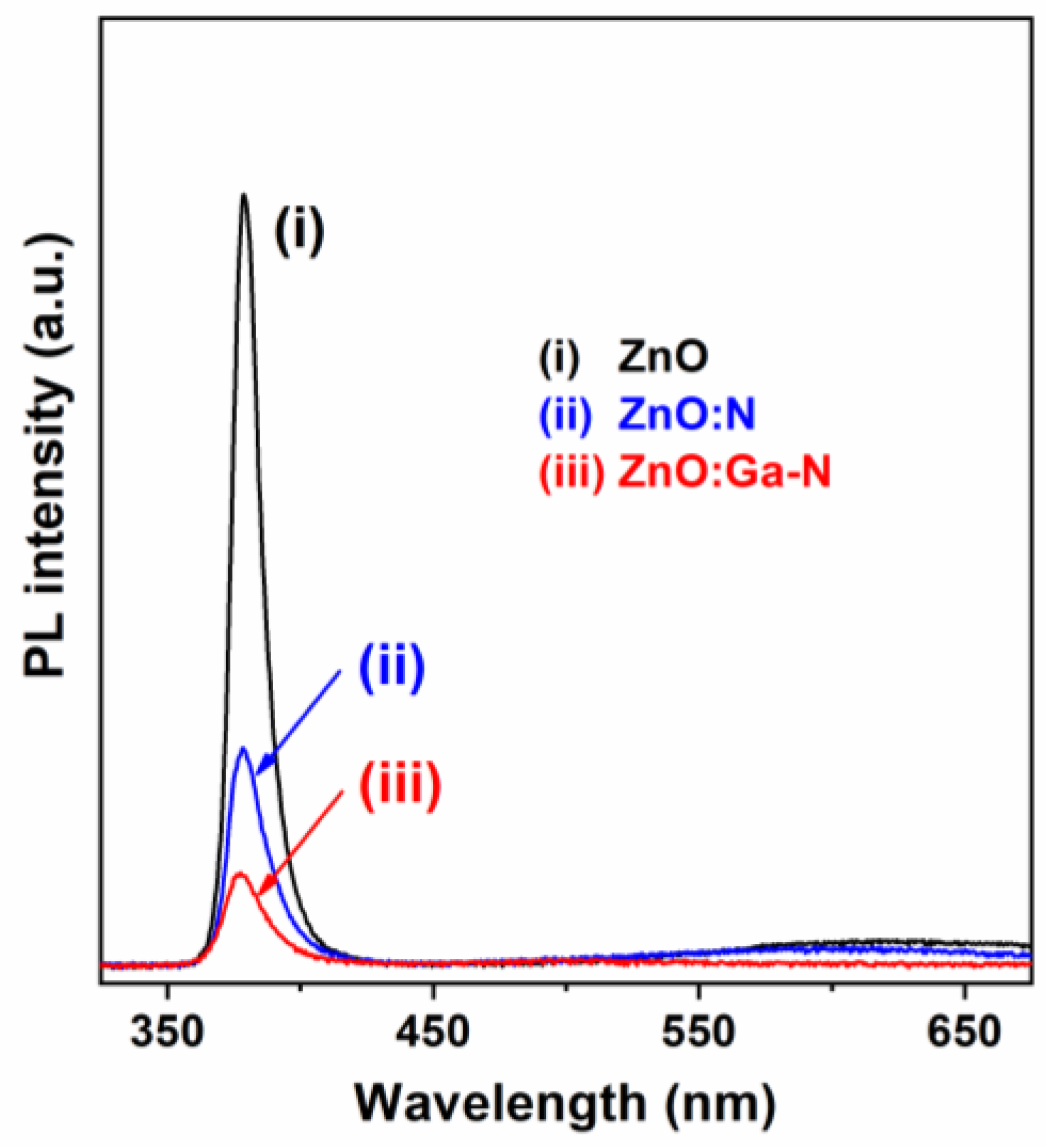
Polycrystalline ZnO thin films exhibit strongly stimulated emissions through excitons even at room temperature, which is one of their unique optical properties [
37]. Two emission signals appeared in each RT PL spectrum (
Figure 6), including a sharp and intense UV emission peak centered at around 379 nm and a weak broad emission band in the visible region. The near-band-edge (NBE) UV emission is created by excitonic emission. A similar UV emission peak (380 nm) has been reported for ZnO thin films deposited on sapphire by sol-gel technique [
32]. It is well known that the broad emission in the visible region is due to deep-level emission related to intrinsic defects such as Zn interstitials and O vacancies. It is worth noting that the decrease in the intensity of NBE emission after doping with N and Ga–N indicated the degeneration of the films’ crystallinity and was ascribed to the increment of non-radiative recombination due to effects induces by N [
22,
24]. The N and Ga–N doping also led to a slight shift in the NBE emission peak as noted in the optical transmittance spectra in the near-UV spectral region. Moreover, the suppression of the visible emission may be attributed to the compensation of intrinsic defects by the acceptor dopants (spectra (ii) and (iii) in
Figure 6). This feature confirmed the greater solubility and stability of the N dopant incorporated in the co-doped ZnO thin film.
Various electrical parameters, including the carrier type, carrier concentration, Hall mobility, and electrical resistivity, of the ZnO-based semiconductor thin films, measured by Hall-effect measurement, are presented in
Table 2. It was confirmed that the pure ZnO thin films had n-type characteristics with a mean electron concentration of 3.19 × 10
15 cm
−3, a mean carrier mobility of 20.77 cm
2/V·s, and a mean resistivity of 94.32 Ω·cm. The measurement results also indicate that the as-prepared ZnO:N thin films exhibited a mean hole concentration of 1.83 × 10
15 cm
−3, a mean hole mobility of 8.85 cm
2/V·s, and a mean resistivity of 385.4 Ω·cm. This change in conductivity type from n to p was related to the incorporation of N dopant into ZnO, which induced shallow acceptors of N
O. However, the hole concentration and resistivity should be improved to achieve device-quality p-type oxide films. It is noted that the mean hole concentration of the p-type ZnO:Ga–N thin films approached 4.0 × 10
17 cm
−3; this magnitude is comparable to those in previous reports on sol-gel-derived Al–N and In–N co-doped p-type ZnO thin films [
22,
24]. In addition, the mobility of the co-doped sample was only about 3.0 cm
2/V·s, possibly due to the formation of the Ga–2N complex; this low mobility caused carrier scattering and restricted the hole mobility. Thus, the hole mobility of the p-type ZnO semiconductor thin films for device applications should be improved in future work.
Ye et al. summarized the electrical properties of several types of group III (B, Al, Ga, and In)–N co-doped p-type ZnO thin films and found that the hole concentration density, Hall mobility, and electrical resistivity were in the ranges of 3 × 10
16 to 5 × 10
18 cm
−3, 0.1 to 15 cm
2/V·s, and 0.015 to 2 × 10
2 Ω·cm, respectively [
7]. The main considerations of the acceptor-donor co-doping method for achieving p-type conduction in ZnO thin films are to lower the ionization energy of acceptors and donors, enhance the solubility of acceptor dopants [
38], and reduce the self-compensation effect to create shallower acceptor levels (falling within the range of 0.1–0.2 eV above the valence-band maximum (VBM)).
For verification of the electrical stability of the p-type oxide thin films, the electrical characteristics were measured in time frames of two to four weeks with periods of 7 days (
Table 2). We found that these p-type ZnO:N thin films reverted to n-type over time. The Ga–N co-doped ZnO thin films exhibited more stable p-type conductivity at 3 weeks than did the N-doped ZnO thin films (<three weeks) due to the formation of the Ga
Zn–N
O pairs, which could offer more efficient incorporation of N dopants and activation of acceptors, and hence the creation of impurity bands above the VBM of ZnO, which increased the hole concentration. A comparison of the electrical characteristics in previous reports on solution-processed group III element (B, Al, In, and Ga)–N co-doped p-type ZnO thin films with those of the developed ZnO:Ga–N thin films in this work is provided in
Table 3. It was found that the electrical properties of ZnO-based thin films fabricated by spray pyrolysis technique are better than those of oxide films prepared by sol-gel process.
The authors examined the optical and electrical properties of the three kinds of sol-gel-derived ZnO-based thin films and connected them with the structural characteristics. Besides comparing the physical properties of the oxide thin films, our experimental investigations clarified the stability of p-type ZnO:N and ZnO:Ga–N thin films. Our study indicates that the p-type ZnO:Ga–N semiconductor thin films exhibited good electrical stability, without significant degeneration of the electrical characteristics, for at least three weeks. We have successfully fabricated Ga–N co-doped ZnO transparent semiconductor thin film, which may be applicable as a stable p-type layer in the development of ZnO-based homojunction or heterojunction electronic and optoelectronic devices.


