
Review of Wafer Surface Defect Detection Methods

Abstract
:1. Introduction
2. Wafer Surface Defect Patterns
3. Wafer Surface Defect Detection Based on Image Signal Processing
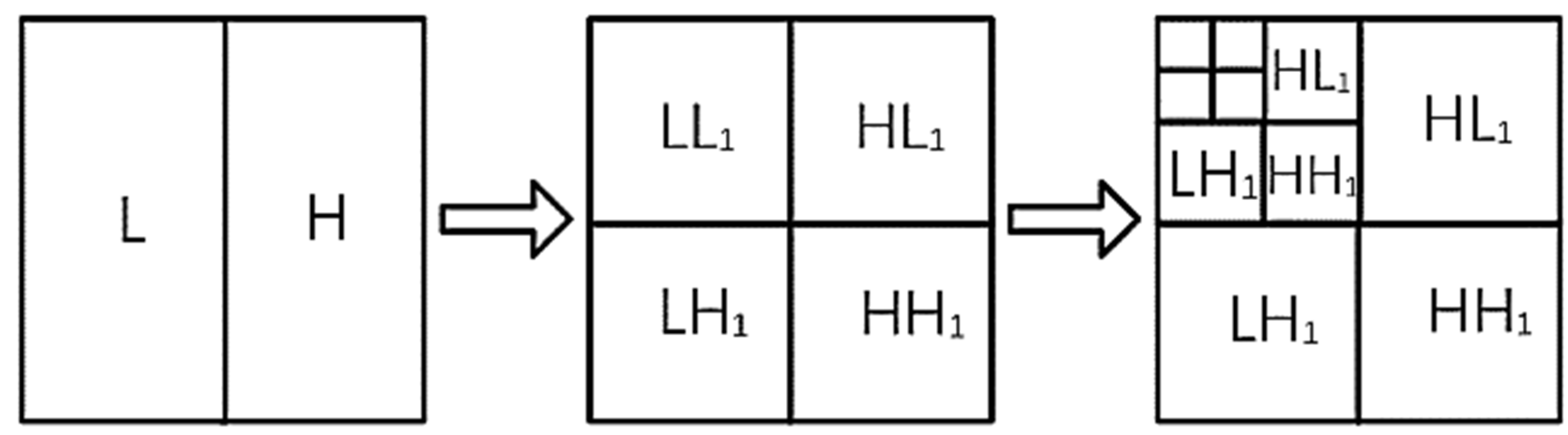
3.1. Wavelet Transform
3.2. Spatial Filtering
3.3. Template Matching
4. Wafer Surface Defect Detection Based on Machine Learning
4.1. Supervised Learning
4.2. Unsupervised Learning
4.3. Semi-Supervised Learning
5. Wafer Surface Defect Detection Based on Deep Learning
5.1. Classification Network
5.2. Object Detection Network
5.3. Segment Network
6. Conclusions and Outlook
- There are few public datasets of wafer defects. Due to the high cost of wafer production and labeling, there are very few high-quality public datasets, and the few datasets are not enough to support training. It is possible to consider creating a synthetic wafer defect database and performing data augmentation on the existing dataset to provide more accurate and comprehensive data samples for neural networks. Due to the versatility of defect types in gradient features, such problems can be addressed using transfer learning, mainly to solve problems such as negative transfer and model inappropriateness in transfer learning [72]. A flexible and efficient migration model does not currently exist. Using transfer learning to solve the problem of a few samples in wafer surface defect detection is a difficult topic for future research.
- During the wafer fabrication process, new defects are continuously generated, and the number and types of defect samples are continuously accumulated. Using incremental learning [73] can improve the recognition accuracy of the network model for new defects and the ability to maintain the classification of old defects. It can also be used as a research direction for the expanded sample method.
- With the rapid development of technological progress, the chip feature size is becoming smaller and more complex, resulting in multiple defect types in a wafer, and the defects are folded with each other, resulting in non-uniform and inconspicuous defect features. increase the difficulty of detection. Multi-step, multi-method hybrid models have become the mainstream method for detecting hybrid defects. How to optimize the performance of the deep network model and maintain a high detection efficiency is a problem that needs to be further solved.
- During the wafer fabrication process, wafer patterns for different purposes will produce different defects. Currently, a network model trained on a single data set is not sufficient to identify defects in all wafers for different purposes. How to design a universal network model to detect all defects, thereby avoiding the waste of resources caused by designing a training model separately for all wafer defect data sets, is a direction worth thinking about in the future.
- The majority of defect detection models are offline models, which are unable to meet the real-time requirements of industrial production. To address this issue, an autonomous learning model system needs to be established, which enables the model to rapidly learn and adapt to new production environments, thereby achieving more efficient and accurate defect detection.
Author Contributions
Funding
Data Availability Statement
Conflicts of Interest
References
- Gao, Y.; Li, X.; Wang, X.V.; Wang, L.; Gao, L. A review on recent advances in vision-based defect recognition towards industrial intelligence. J. Manuf. Syst. 2021, 62, 753–766. [Google Scholar] [CrossRef]
- Zhu, Y.; Ling, Z.; Zhang, Y. Research progress and Prospect of machine vision technology. J. Graph. 2020, 41, 871–890. [Google Scholar]
- Kim, T.; Behdinan, K. Advances in Machine Learning and Deep Learning Applications towards Wafer Map Defect Recognition and Classification: A Review. J. Intell. Manuf. 2022, 33, 1805–1826. [Google Scholar] [CrossRef]
- Thomas, N.; Wong, H.S.P. The End of Moore’s Law: A New Beginning for Information Technology. Comput. Sci. Eng. 2017, 19, 41–50. [Google Scholar]
- Zhu, J.; Liu, J.; Xu, T.; Yuan, S.; Zhang, Z.; Jiang, H.; Gu, H.; Zhou, R.; Liu, S. Optical Wafer Defect Inspection at the 10 nm Technology Node and Beyond. Int. J. Extrem. Manuf. 2022, 12, 2631–8644. [Google Scholar] [CrossRef]
- McLaughlin, M.P.; Mennell, P.; Stamper, A.; Barber, G.; Paduano, J.; Benn, E.; Linnane, M.; Zwick, J.; Khatumria, C.; Isaacson, R.L.; et al. Improved Color Defect Detection with Machine Learning for After Develop Inspections in Lithography. IEEE Trans. Semicond. Manuf. 2022, 35, 418–424. [Google Scholar] [CrossRef]
- Chen, S.H. Research on Machine Learning and Intelligent Classification and Identification of Wafer Defect Patterns in Microelectronics Manufacturing. Ph.D. Thesis, Jiangsu University, Zhenjiang, China, 2021. [Google Scholar]
- Hansen, M.H.; Nair, V.N.; Friedman, D.J. Monitoring wafer map data from integrated circuit fabrication processes for spatially clustered defects. Technometrics 1997, 39, 241–253. [Google Scholar] [CrossRef]
- Jeong, Y.-S.; Kim, S.J.M. Automatic Identification of Defect Patterns in Semiconductor Wafer Maps Using Spatial Correlogram and Dynamic Time Warping. IEEE Trans. Semicond. Manuf. 2008, 21, 625–637. [Google Scholar] [CrossRef]
- Mirza, A.I.; O’Donoghue, G.; Drake, A.W.; Graves, S.C. Spatial yield modeling for semiconductor wafers. In Proceedings of the SEMI Advanced Semiconductor Manufacturing Conference and Workshop, Cambridge, MA, USA, 13–15 November 1995; pp. 276–281. [Google Scholar]
- Wu, M.J.; Jang, J.S.R.; Chen, J.L. Wafer Map Failure Pattern Recognition and Similarity Ranking for Large-Scale Data Sets. IEEE Trans. Semicond. Manuf. 2014, 28, 1–12. [Google Scholar]
- Kim, Y.; Cho, D.; Lee, J.H. Wafer map classifier using deep learning for detecting out-of-distribution failure patterns. In Proceedings of the 2020 IEEE International Symposium on the Physical and Failure Analysis of Integrated Circuits (IPFA), Singapore, 20–23 July 2020; pp. 1–5. [Google Scholar]
- Kang, S.; Cho, S.; An, D.; Rim, J. Using wafer map features to better predict die-level failures in final test. IEEE Trans. Semicond. Manuf. 2015, 28, 431–437. [Google Scholar] [CrossRef]
- Saqlain, M.; Jargalsaikhan, B.; Lee, J.Y. A voting ensemble classifier for wafer map defect patterns identification in semiconductor manufacturing. IEEE Trans. Semicond. Manuf. 2019, 32, 171–182. [Google Scholar] [CrossRef]
- Shim, J.; Kang, S.; Cho, S. Active learning of convolutional neural network for cost-effective wafer map pattern classification. IEEE Trans. Semicond. Manuf. 2020, 33, 258–266. [Google Scholar] [CrossRef]
- Feng, L. Research on Wafer Defects in Semiconductor Lithography. Master’s Thesis, Tianjin University, Tianjin, China, 2021. [Google Scholar]
- Caiazzo, F.; Gao, R.; Teti, R. Machine learning-based image processing for on-line defect recognition in additive manufacturing. CIRP Ann. 2019, 68, 451–454. [Google Scholar]
- Zhang, H. Research on the Optimizing Process of the Basic Image Processing Algorithms. In Proceedings of the International Conference on Cyber Security Intelligence and Analytics, Shenyang, China, 21–22 February 2019; pp. 212–217. [Google Scholar]
- Rajeswari, J.; Jagannath, M. Advances in biomedical signal and image processing—A systematic review. Inform. Med. Unlocked 2017, 8, 13–19. [Google Scholar]
- Guo, T.; Zhang, T.; Lim, E.; Lopez-Benitez, M.; Ma, F.; Yu, L. A Review of Wavelet Analysis and Its Applications: Challenges and Opportunities. IEEE Access 2022, 10, 58869–58903. [Google Scholar] [CrossRef]
- Wang, F.; Liu, Q.; Hu, D.; Wang, Y.; Zheng, T. Research of the image restoration algorithm based on boundary pre-processing in the space domain and fast computing in the frequency domain. In Proceedings of the Fifth Symposium on Novel Optoelectronic Detection Technology and Application, Xi’an, China, 12 March 2019; Volume 11023, pp. 143–154. [Google Scholar]
- Prasath, V.B.S.; Thanh, D.N.H.; Hung, N.Q.; Hieu, L.M. Multiscale gradient maps augmented fisher information-based image edge detection. IEEE Access 2020, 8, 141104–141110. [Google Scholar] [CrossRef]
- Yeh, C.H.; Wu, F.C.; Ji, W.L.; Huang, C.Y. A wavelet-based approach in detecting visual defects on semiconductor wafer dies. IEEE Trans. Semicond. Manuf. 2010, 23, 284–292. [Google Scholar] [CrossRef]
- Yang, W.R. Short-time discrete wavelet transform for wafer microcrack detection. In Proceedings of the 2009 IEEE International Symposium on Industrial Electronics, Seoul, Republic of Korea, 5–8 July 2009. [Google Scholar]
- Villa, J.; González, E.; Moreno, G.; de la Rosa, I.; Flores, J.L.; Alaniz, D. Fringe pattern denoising using spatial oriented gaussian filters. Opt. Commun. 2020, 457, 124704. [Google Scholar] [CrossRef]
- Allen, J.; Brewster, C.; Slone, D. Spatially explicit ecological models: A spatial convolution approach. Chaos Solitons Fractals 2001, 12, 333–347. [Google Scholar] [CrossRef]
- Kuan, D.T.; Sawchuk, A.A.; Strand, T.C.; Chavel, P. Adaptive noise smoothing filter for images with signal-dependent noise. IEEE Trans. Pattern Anal. Mach. Intell. 1985, 221, 165–177. [Google Scholar] [CrossRef]
- Zhang, B.; Allebach, J.P. Adaptive bilateral filter for sharpness enhancement and noise removal. IEEE Trans. Image Process. 2008, 17, 664–678. [Google Scholar] [CrossRef] [PubMed]
- Ohshige, T.; Tanaka, H.; Miyazaki, Y.; Kanda, T.; Ichimura, H.; Kosaka, N.; Tomoda, T. Defect inspection system for patterned wafers based on the spatial-frequency filtering. In Proceedings of the 1991 Proceedings Eleventh IEEE/CHMT International Electronics Manufacturing Technology Symposium, San Francisco, CA, USA, 16–18 September 1991. [Google Scholar]
- Wang, C.H. Recognition of semiconductor defect patterns using spatial filtering and spectral clustering. Expert Syst. Appl. 2008, 34, 1914–1923. [Google Scholar] [CrossRef]
- Zarinbal, M.; Zarandi, M.F.; Turksen, I. Relative entropy fuzzy c-means clustering. Inf. Sci. 2014, 260, 74–79. [Google Scholar] [CrossRef]
- Jia, H.; Ding, S.; Xu, X.; Nie, R. The latest research progress on spectral clustering. Neural. Comput. Appl. 2014, 24, 1477–1486. [Google Scholar] [CrossRef]
- Chen, S.H.; Kang, C.H.; Perng, D.B. Detecting and measuring defects in wafer die using gan and yolov3. Appl. Sci. 2020, 10, 8725. [Google Scholar] [CrossRef]
- Briechle, K.; Hanebeck, U.D. Template matching using fast normalized cross correlation. In Optical Pattern Recognition XII; SPIE: Bellingham, WA, USA, 2001; Volume 4387, pp. 95–102. [Google Scholar]
- Brunelli, R. Template Matching Techniques in Computer Vision: Theory and Practice; John Wiley & Sons: Hoboken, NJ, USA, 2009. [Google Scholar]
- Han, H.; Gao, C.; Zhao, Y.; Liao, S.; Tang, L.; Li, X. Polycrystalline silicon wafer defect segmentation based on deep convolutional neural networks. Pattern Recognit. Lett. 2020, 130, 234–241. [Google Scholar] [CrossRef]
- Khalaj, B.H.; Aghajan, H.K.; Kailath, T. Digital image processing techniques for patterned-wafer inspection. In Proceedings of the SPIE’S 1993 Symposium on Microlithography, San Jose, CA, USA, 4 August 1993; Volume 1926, pp. 508–516. [Google Scholar]
- Kotsiantis, S.B.; Zaharakis, I.; Pintelas, P. Supervised machine learning: A review of classification techniques. Emerg. Artif. Intell. Appl. Comput. Eng. 2007, 160, 3–24. [Google Scholar]
- Kotsiantis, S.B.; Zaharakis, I.D.; Pintelas, P.E. Machine learning: A review of classification and combining techniques. Artif. Intell. Rev. 2006, 26, 159–190. [Google Scholar] [CrossRef]
- Yuan, T.; Kuo, W.; Bae, S.J. Detection of spatial defect patterns generated in semiconductor fabrication processes. IEEE Trans. Semicond. Manuf. 2011, 24, 392–403. [Google Scholar] [CrossRef]
- Piao, M.; Jin, C.H.; Lee, J.Y.; Byun, J.Y. Decision tree ensemble-based wafer map failure pattern recognition based on radon transform-based features. IEEE Trans. Semicond. Manuf. 2018, 31, 250–257. [Google Scholar] [CrossRef]
- Burges, C.J. A tutorial on support vector machines for pattern recognition. Data Min. Knowl. Discov. 1998, 2, 121–167. [Google Scholar] [CrossRef]
- Xie, L.; Li, D.; Simske, S.J. Feature dimensionality reduction for example-based image super-resolution. J. Pattern Recognit. Res. 2011, 6, 130–139. [Google Scholar] [CrossRef] [PubMed] [Green Version]
- Song, H.; Choi, K.K.; Lee, I.; Zhao, L.; Lamb, D. Adaptive virtual support vector machine for reliability analysis of high-dimensional problems. Struct. Multidiscip. Optim. 2013, 47, 479–491. [Google Scholar] [CrossRef]
- Baly, R.; Hajj, H. Wafer classification using support vector machines. IEEE Trans. Semicond. Manuf. 2012, 25, 373–383. [Google Scholar] [CrossRef]
- Xie, L.; Huang, R.; Gu, N.; Cao, Z. A novel defect detection and identification method in optical inspection. Neural Comput. Appl. 2014, 24, 1953–1962. [Google Scholar] [CrossRef]
- Barlow, H.B. Unsupervised learning. Neural Comput. 1989, 1, 295–311. [Google Scholar] [CrossRef]
- Huang, C.J. Clustered defect detection of high quality chips using self-supervised multilayer perceptron. Expert Syst. Appl. 2007, 33, 996–1003. [Google Scholar] [CrossRef]
- Jin, C.H.; Na, H.J.; Piao, M.; Pok, G.; Ryu, K.H. A novel DBSCAN-based defect pattern detection and classification framework for wafer bin map. IEEE Trans. Semicond. Manuf. 2019, 32, 286–292. [Google Scholar] [CrossRef]
- Di Palma, F.; De Nicolao, G.; Miraglia, G.; Pasquinetti, E.; Piccinini, F. Unsupervised spatial pattern classification of electrical-wafer-sorting maps in semiconductor manufacturing. Pattern Recognit. Lett. 2005, 26, 1857–1865. [Google Scholar] [CrossRef]
- Xiaoxi, W.; Wenjun, W.; Feng, Y.; Pengbo, S.; Xuanyi, Z.; Yanhua, Z. Pseudo-label based semi-supervised learning in the distributed machine learning framework. High Technol. Lett. 2022, 28, 172–180. [Google Scholar]
- Li, K.S.M.; Jiang, X.H.; Chen, L.L.Y.; Wang, S.J.; Huang, A.Y.A.; Chen, J.E.; Liang, H.C.; Hsu, C.L. Wafer Defect Pattern Labeling and Recognition Using Semi-Supervised Learning. IEEE Trans. Semicond. Manuf. 2022, 35, 291–299. [Google Scholar] [CrossRef]
- Kong, Y.; Ni, D. A semi-supervised and incremental modeling framework for wafer map classification. IEEE Trans. Semicond. Manuf. 2020, 33, 62–71. [Google Scholar] [CrossRef]
- Albawi, S.; Mohammed, T.A.; Al-Zawi, S. Understanding of a convolutional neural network. In Proceedings of the 2017 International Conference on Engineering and Technology (ICET), Antalya, Turkey, 21–23 August 2017; pp. 1–6. [Google Scholar]
- Cheng, K.C.C.; Chen, L.L.Y.; Li, J.W.; Li, K.S.M.; Tsai, N.C.Y.; Wang, S.J.; Huang, A.Y.A.; Chou, L.; Lee, C.S.; Chen, J.E.; et al. Machine learning-based detection method for wafer test induced defects. IEEE Trans. Semicond. Manuf. 2021, 34, 161–167. [Google Scholar] [CrossRef]
- Wright, R.E. Logistic Regression. 1995. Available online: https://psycnet.apa.org/record/1995-97110-007 (accessed on 5 February 2023).
- Chen, Y.; Zhou, X.S.; Huang, T.S. One-class SVM for learning in image retrieval. In Proceedings of the 2001 International Conference on Image Processing (Cat. No. 01CH37205), Thessaloniki, Greece, 7–10 October 2001; Volume 1, pp. 34–37. [Google Scholar]
- Song, Y.Y.; Ying, L. Decision tree methods: Applications for classification and prediction. Shanghai Arch. Psychiatry 2015, 27, 130. [Google Scholar] [PubMed]
- Ma, W.; Lu, J. An equivalence of fully connected layer and convolutional layer. arXiv 2017, arXiv:1712.01252 2017. [Google Scholar]
- Wang, J.; Xu, C.; Yang, Z.; Zhang, J.; Li, X. Deformable convolutional networks for efficient mixed-type wafer defect patternrecognition. IEEE Trans. Semicond. Manuf. 2020, 33, 587–596. [Google Scholar] [CrossRef]
- Kyeong, K.; Kim, H. Classification of mixed-type defect patterns in wafer bin maps using convolutional neural networks. IEEE Trans. Semicond. Manuf. 2018, 31, 395–402. [Google Scholar] [CrossRef]
- Nakazawa, T.; Kulkarni, D.V. Wafer map defect pattern classification and image retrieval using convolutional neural network. IEEE Trans. Semicond. Manuf. 2018, 31, 309–314. [Google Scholar] [CrossRef]
- Girshick, R.; Donahue, J.; Darrell, T.; Malik, J. Rich feature hierarchies for accurate object detection and semantic segmentation. In Proceedings of the IEEE Conference on Computer Vision and Pattern Recognition, Washington, DC, USA, 23–28 June 2014; pp. 580–587. [Google Scholar]
- Ren, S.; He, K.; Girshick, R.; Sun, J. Faster r-cnn: Towards real-time object detection with region proposal networks. Adv. Neural Inf. Process. Syst. 2015, 39, 1137–1149. [Google Scholar] [CrossRef] [Green Version]
- Redmon, J.; Divvala, S.; Girshick, R.; Farhadi, A. You only look once: Unified, real-time object detection. In Proceedings of the IEEE Conference on Computer Vision and Pattern Recognition, Las Vegas, NV, USA, 27–30 June 2016; pp. 779–788. [Google Scholar]
- Redmon, J.; Farhadi, A. YOLO9000: Better, faster, stronger. In Proceedings of the IEEE Conference on Computer Vision and Pattern Recognition, Honolulu, HI, USA, 21–26 June 2017; pp. 7263–7271. [Google Scholar]
- Redmon, J.; Farhadi, A. Yolov3: An incremental improvement. arXiv 2018, arXiv:1804.02767 2018. [Google Scholar]
- Yu, J.; Liu, J. Two-dimensional principal component analysis-based convolutional autoencoder for wafer map defect detection. IEEE Trans. Ind. Electron. 2020, 68, 8789–8797. [Google Scholar] [CrossRef]
- Shinde, P.P.; Pai, P.P.; Adiga, S.P. Wafer Defect Localization and Classification Using Deep Learning Techniques. IEEE Access 2022, 10, 39969–39974. [Google Scholar] [CrossRef]
- Nakazawa, T.; Kulkarni, D.V. Anomaly detection and segmentation for wafer defect patterns using deep convolutional encoder–decoder neural network architectures in semiconductor manufacturing. IEEE Trans. Semicond. Manuf. 2019, 32, 250–256. [Google Scholar] [CrossRef]
- Nag, S.; Makwana, D.; Mittal, S.; Mohan, C.K. A light-weight network for classification and segmentation of semiconductor wafer defects. Comput. Industry 2022, 142, 103720. [Google Scholar] [CrossRef]
- Torrey, L.; Shavlik, J. Handbook of Research on Machine Learning Applications and Trends: Algorithms, Methods, and Techniques; Information Science Reference: Hershey, PA, USA, 2010. [Google Scholar]
- Castro, F.M.; Marín-Jiménez, M.J.; Guil, N.; Schmid, C.; Alahari, K. End-to-end incremental learning. In Proceedings of the European Conference on Computer Vision (ECCV), Munich, Germany, 8–14 October 2018; pp. 233–248. [Google Scholar]


| Model Algorithm | Innovation | Limitation |
|---|---|---|
| Wavelet transform [12,20,21,22,23,24] | The image can be decomposed into multiple resolutions and presented as local sub-images with different spatial frequencies. Anti-grain. | The selection of the threshold is very dependent and the adaptability is poor. |
| Spatial filtering [25,26,27,28,29,30,31,32,33] | Based on spatial convolution, remove high-frequency noise, and perform edge enhancement. | Performance depends on the threshold parameter. |
| Template matching [11,17,34,35,36] | The template matching algorithm has strong anti-noise ability and fast calculation speed. | Sensitive to feature object size. |
| Classification | Algorithm | Innovation | Limitation |
|---|---|---|---|
| Supervised learning [38,39,40,41,42,43,4445,46] | KNN | Insensitive to abnormal data and highly accurate. | High complexity and computation intensity. |
| Decision Tree-Radon | Apply Radon to form new defect features. | Overfitting is highly proficient. | |
| SVM | SVM efficiently classifies multivariate, multi-modal, and indivisible data points. | It is not friendly to multiple samples, and the kernel function is difficult to locate. | |
| Unsupervised learning [47,48,49,50] | Multilayer Perceptron-Clustering Algorithm | The multilayer perceptron is used to enhance the feature extraction capability. | Depends on the choice of activation function. |
| DBSCAN | Outliers can be selectively removed based on defect pattern characteristics. | The sample density is not uniform or the sample is too large, the convergence time is long, and the clustering effect is poor. | |
| SOM | High-dimensional data can be mapped to a low dimensional space and the structure of the high-dimensional space can be maintained. | The objective function is not easy to determine. | |
| Semi-supervised learning [51,52,53] | A semi-supervised framework for augmented labeling | A semi-supervised model is built by combining supervised ensemble learning and unsupervised SOM. | Training is time-consuming and time-consuming. |
| Semi-Supervised Increment-al Modeling Framework | Improve model performance by actively learning and labeling samples to enhance them. | Performance depends on the amount of data tagged. |
| Algorithm | Innovation | Acc |
|---|---|---|
| DC-Net [60] | The sampling area is focused on the defect feature area, which is very robust to mixed defects. | 93.2% |
| CNN-Based Combined Classifier [61] | Separately design classifiers for each defect, strong adaptability to new defect modes. | 97.4% |
| Classification Retrieval Method Based on CNN [62] | Simulated datasets can be generated to account for data imbalances. | 98.2% |
| Algorithm | Innovation | Acc | Ap |
|---|---|---|---|
| PCACAE [68] | Automatic coding of concatenated roll types based on two-dimensional principal component analysis. | 97.27% | \ |
| YOLOv3-GAN [33] | GAN enhances the diversity of defect patterns and improves the versatility of YOLOv3. | \ | 88.72% |
| YOLOv4 [69] | Updated backbone network, enhanced with CutMix and Mosaic data. | 94.0% | 75.8% |
| Algorithm | Innovation | Acc |
|---|---|---|
| FCN [62] | Replacing fully connected layers with convolutional layers to output 2D heatmaps. | 97.8% |
| SegNet [62] | Combining encoder–decoder and pixel-level classification layers. | 99.0% |
| U-net [36] | Copy and crop the feature maps in each encoder layer to the corresponding decoder layer. | 98.9% |
| WaferSegClassNet [70] | Simultaneous classification and Segmentation using shared encoders. | 98.2% |
Disclaimer/Publisher’s Note: The statements, opinions and data contained in all publications are solely those of the individual author(s) and contributor(s) and not of MDPI and/or the editor(s). MDPI and/or the editor(s) disclaim responsibility for any injury to people or property resulting from any ideas, methods, instructions or products referred to in the content. |
© 2023 by the authors. Licensee MDPI, Basel, Switzerland. This article is an open access article distributed under the terms and conditions of the Creative Commons Attribution (CC BY) license (https://creativecommons.org/licenses/by/4.0/).
Share and Cite
Ma, J.; Zhang, T.; Yang, C.; Cao, Y.; Xie, L.; Tian, H.; Li, X. Review of Wafer Surface Defect Detection Methods. Electronics 2023, 12, 1787. https://doi.org/10.3390/electronics12081787
Ma J, Zhang T, Yang C, Cao Y, Xie L, Tian H, Li X. Review of Wafer Surface Defect Detection Methods. Electronics. 2023; 12(8):1787. https://doi.org/10.3390/electronics12081787
Chicago/Turabian StyleMa, Jianhong, Tao Zhang, Cong Yang, Yangjie Cao, Lipeng Xie, Hui Tian, and Xuexiang Li. 2023. "Review of Wafer Surface Defect Detection Methods" Electronics 12, no. 8: 1787. https://doi.org/10.3390/electronics12081787
APA StyleMa, J., Zhang, T., Yang, C., Cao, Y., Xie, L., Tian, H., & Li, X. (2023). Review of Wafer Surface Defect Detection Methods. Electronics, 12(8), 1787. https://doi.org/10.3390/electronics12081787