1. Introduction
Plasma is an ionized gas, into which sufficient energy is provided to free electrons from atoms or molecules. It sometimes allow species, ions, and electrons to coexist [
1]. The most important thing is that plasmas are the high common state of matter in the universe and even on earth. Plasma is a gas that has been energized to the point that some of the electrons break free from, but travel with, their nucleus. Gases can become plasmas in several ways, but all include pumping the gas with energy. A spark in a gas will create plasma. Plasma is an electrically inoffensive medium of unbound positive and negative particles. Although they are not ‘free’ in the sense of not experiencing forces. Moving charged particles generate an electric current within a magnetic field, and any movement of a charged plasma particle affects and is affected by the fields created by the other charges. In turn, this governs collective behavior with many degrees of variation [
2,
3].
Basically, plasma is generated artificially in the laboratory or industry by the application of an electric or magnetic field through a gas. Although there are several means for plasma generation, in all cases, there must be a plasma power source to produce and sustain it [
4]. Plasma can apply a voltage, and subsequently ionization can occur, as shown in
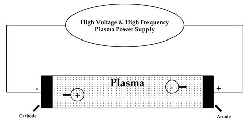
Figure 1, which presents a discharge tube as a simple example. The potential difference and subsequent electric field pull the bound electrons toward the anode, while the cathode pulls the nucleus [
5]. As the voltage is increased, the current stresses the material by increasing electric polarization. Once the polarization exceeds the dielectric limit, electrical breakdown occurs, where the material transforms from being an insulator to a conductor. The underlying fundamental process is called an avalanche, where collisions between electrons and neutral gas atoms produce more ions and electrons.
Plasma requires high voltage high frequency (HVHF) switching power supply as a source. HVHF is being used for many industrial applications [
6,
7,
8], such as water purification, static charge removers, fluorescent tubes, plasma arc welding, plasma cutting, textiles, surface modification [
9,
10], biomedical applications [
11,
12,
13], plasma displays, radicals, plasma needles [
14], corona discharges [
15], medical applications, and ozone generators [
16]. Medical uses are an exciting new area for plasma applications that can be used in the treatment of diseases and cancer. In essence, the ozone generator is used for sterilization [
17] and imprinting plastic and metal items, and involves the ionization of air. Ozone is produced in nature in two ways: corona discharge and ion propulsion method. A corona discharge in nature is called a lightning strike caused by a high voltage DC discharge of electricity. Ion propulsion is another interesting method in near future plasma applications, because it allows spacecraft to travel vast distances.
Various power sources, such as DC, RF, and microwave, are being developed in laboratories and industries to generate electrical current by applying very high voltage high frequency electric fields through a gas. On the other hand, the operation of plasma sources has different requirements according to the applications. Therefore, in most cases, to match with the application requirements, different voltages and different frequency pulsating DC systems are being developed for generating required electric filed to produce electric current. In the present study, a high voltage high frequency plasma power supply was presented, which produces the essential plasma source for water purification in industrial applications [
18,
19,
20]. In this design, we use a modulation index technique that controls the amplitude and frequency.
According to review [
21], Weltmann and Woedtke designed the plasma source for sterilizing medical devices. They developed a high voltage and high frequency plasma source using a pulsed sinusoidal voltage of 10 kV/20 kHz. A high voltage and high frequency power supply was designed for an ozone generator, which is one of the plasma applications, for use in air and water disinfection [
22]. This laboratory-built power supply using a high voltage ferrite transformer and a PLC microcontroller was used to energize a dielectric barrier discharge ozone generator. Cui jiuxia et al. designed a high voltage power supply for electro curtain applications [
23]. The developed circuits achieved a high power factor, high efficiency, rapid fault response, and low ripple systems. For plasma torch applications, a high power converter circuit was designed, including a rectifier and filter system, and a converter circuit was designed using ferrite material with high frequency and output voltage with a rapid time [
24]. For plasma immersion ion implantation applications, they designed pulsed modulators with a high voltage system. A PLC-based pulse modulator and PLC driving system is presented, and the PLC system is very powerful for optimizing ion-implantation. The protection circuit was also designed for short circuits [
25]. The other proposal is for surface treatment by plasma immersion ion implantation. This design consists of three basic circuits: pulse forming network, hard-tube pulsar, and Blumlein line [
26].
The authors of [
27] demonstrate the advantages of parallel and series configuration of flyback converters for pulsed power applications. Thus, the concept is to increase the voltage level and rise time of the generated pulses while emphasizing the modularity concept. There are two kinds of experimental sections that occured, one is 4 kV output voltage and other is 20 kV output voltage, while the repetition rate of frequency is 1 kHz. On other hand, the authors of [
28] demonstrate how the proposed topology operates independently from the load while preserving high repetition rate. The control algorithm is designed in a way that it can prevent from any possible faults and protect the system from the over-voltage. The designed system is between 1 kV and 3 kV with different circumstances. We presented high voltage high frequency plasma power supply with 10 kV, 5 kW, and 25 kHz; repetition rate of frequency is high. We presented both voltage and current protection circuits to prevent the system from having any issues. Mainly, this plasma power supply presents the line regulation circuit to maintain a stable output regardless of changes in the input voltage, load, or connected device.
In the work of [
29], the experimentations have been conducted based on a high-voltage DC power supply and a high-voltage pulse generator for point-to-point and point-to-plane geometries. In addition to the employed geometry, the ambient also plays an important role on electric field formation. Thus, the electric field distribution was simulated for both aforementioned geometries in air–water medium. In this case, the high electric field strength for both geometries appears across the point electrode. This is because of the fact that the water conductivity makes the electric field distribution for both geometries almost similar. Here, the water conductivity was selected to be 200 µS/cm, the same as the tap water used in the experimentation phase. In this research paper, gas can produce an electric or a magnetic field in plasma. We presented the plasma power supply with 10 kV
p-p, which is applied to the plasma load for water purification. The pros of the design are simplicity, cost-efficiency, and quick purifying of the water. The cons of the system are heat, explosion risk, and its time-consuming nature.
The plasma has requirements based on the applications. For example, the helicon plasma will work at 13.56 MHz with radio frequency levels up to 120 kW; microwaves at 28 GHz, which requires up to 30 kW; and ion cyclotron heating operates at 7–9 MHz, which will work until 30 kW [
30]. This paper presented a fully analog-controlled high voltage high frequency (HVHF) plasma switching power supply. The developed HVHF topology applies for water purification in industry. Water purification is the kind of removing dust particles, undesirable chemicals, suspended solids, and gases from water. The goal is to produce water for a specific purpose. Most water is disinfected for human consumption, but water purification may also be designed for a variety of other purposes, including fulfilling the requirements of medical, pharmacological, chemical, and industrial applications.
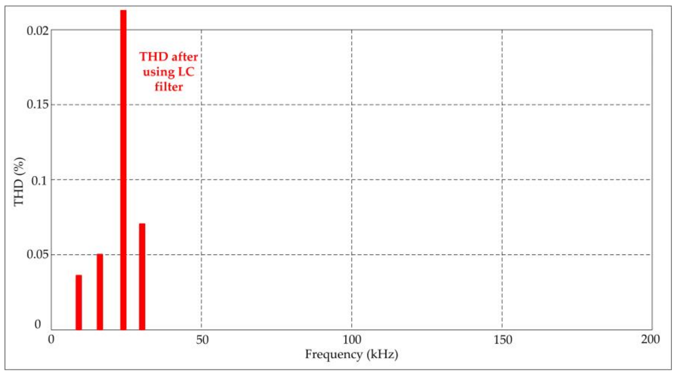
There are some plasma technologies that are regularly used for water purification, such as ozone, electron beam, and electrical discharge. We presented the electrical discharge technique, which generates ions and electrons with very high energy as active species. The active species will remove the dust particles and unwanted waste particles. Because of their physical and chemical properties, the substantial amount used for the electrodes affects the chemical process of plasma in water, necessitating a study of difference in electrode substantial in plasma discharge used in organic solution removal. The objective of this work is explained on water purification by plasma technology has been presented and experimentally verified. A plasma power supply with an output voltage of 10 kV was connected to the plasma load to start the electrical discharge. In this design, the input of 200 V AC to 240 V AC is applied to the plasma power supply and will generate 10 kVp-p alternating current. This high voltage of AC is connected to the plasma load, which is applied to the water. The effects of variable modulation index on the total harmonic distortion (THD) content of the resulting inverter output are studied.
The 10 kV, 5 kW presented 4T analog MOS control HVHF plasma switching power supply was developed in the laboratory and a generated high frequency electric field was applied, which produces the required electric power for plasma.
Section 2 presents a detailed explanation of the HVHF power supply, which is a combination of diode bridge rectifier, high voltage and high frequency PWM inverter, high frequency transformer, filter design, and line-regulation. The modulation technique is explained in
Section 3. The experimental setup of the HVHF power supply and practical work are reported in
Section 4. The experiment results and discussion on the HVHF with the power conversion efficiency of design are presented in
Section 5. Finally,
Section 6 reports the conclusions on research and development of the system.
2. High Voltage High Frequency Plasma Power Supply
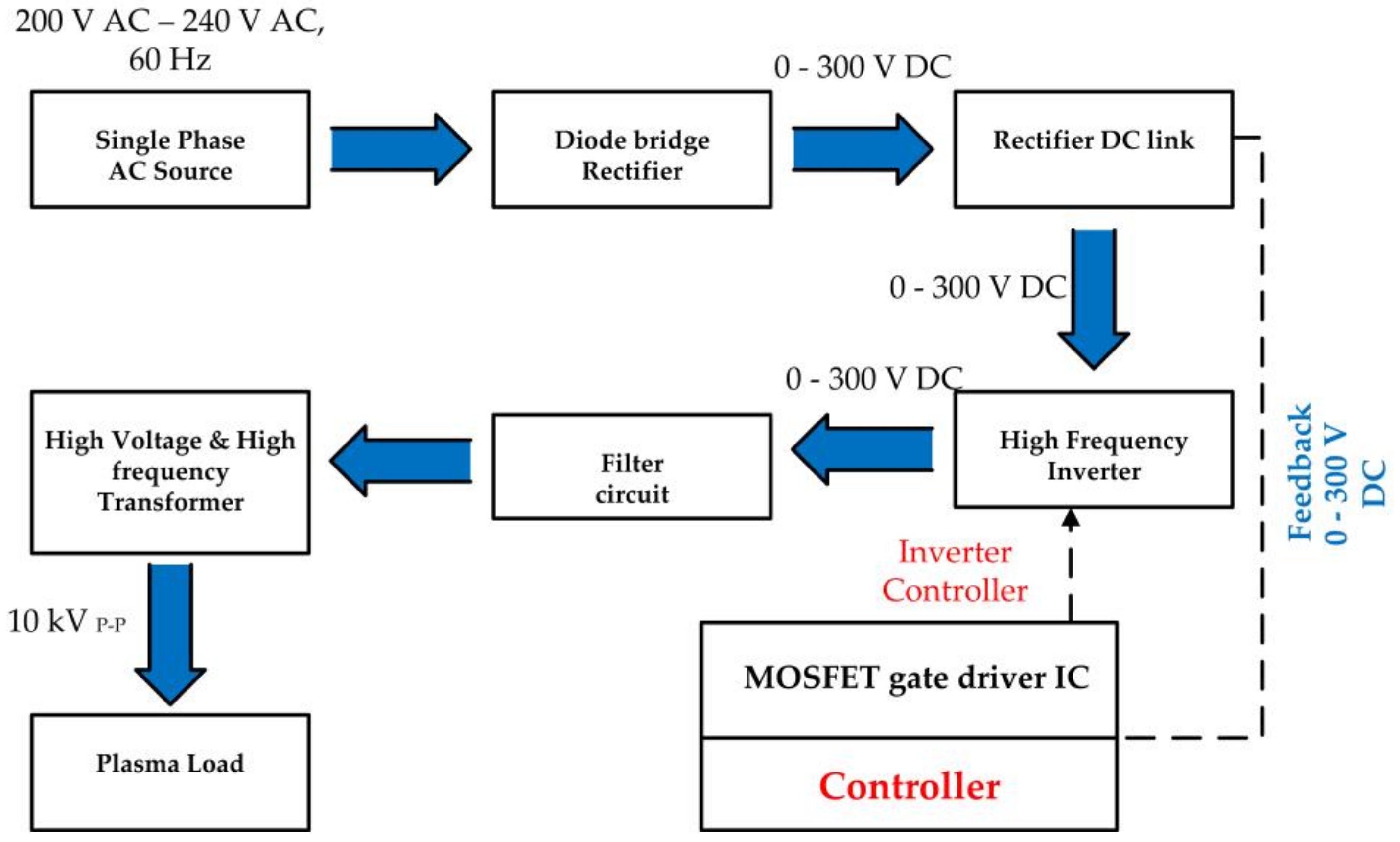
The block diagram of the HVHF plasma switching power supply is shown in
Figure 2. A single phase AC source was applied as the input to the designed power supply. A diode full bridge rectifier circuit was designed as the initial stage of the plasma power supply. The circuit rectifies the 220 V AC voltage to DC output voltage [
31,
32,
33,
34,
35,
36,
37,
38,
39], which can be adjusted from 0 V to 300 V. A high frequency inverter circuit was designed and located, following by the rectifier DC link capacitor, which receives the DC voltage from the rectifier and converts it to a high frequency pulsating DC output voltage. The full-bridge PWM topology with high switching frequency was developed as an inverter circuit for the designed plasma power supply. A high voltage and high frequency transformer was designed and placed at the output of the inverter side. The high frequency pulsating DC output was connected to the primary side of the transformer. The transformer was designed with a ferrite PL-13 U core that could transform 290–300 V to 10 kV high voltage. The secondary side of the transformer that transformed the high voltage was connected to the plasma source, which was designed with titanium, quartz tube, and metal.
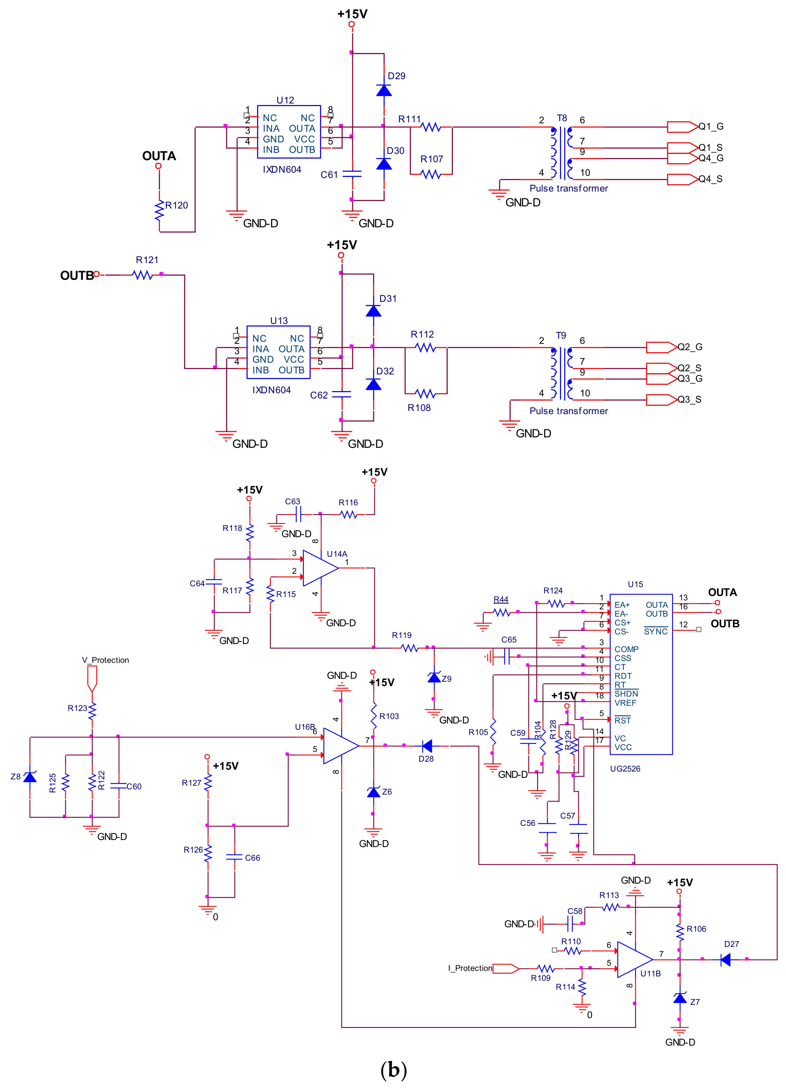
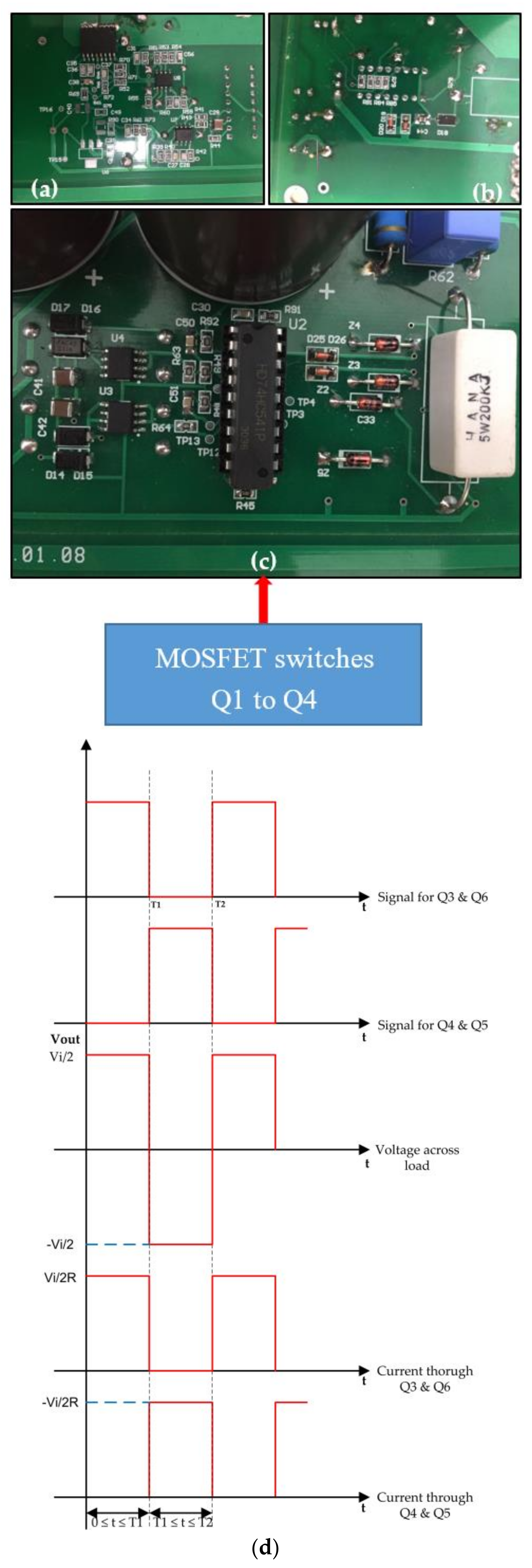
Figure 3 shows the schematic diagram of 4T analog MOS control plasma switching power supply. The single phase AC voltage was applied to the circuit. The GBJ2506 bridge rectifier was used along with the DC link capacitors. The designed rectifier full bridge consisted of four diodes that were arranged as shown in
Figure 3.
2.1. High Voltage High Frequency PWM Inverter
A high switching frequency high power PWM inverter circuit was designed and placed followed by the rectifier of the plasma power supply, as shown in
Figure 3. The IXFK64N50P MOSFET was used as a switching device in the PWM full bridge inverter. The chosen MOSFET allowed a 500 V and 64 A maximum. This has a lower drain source resistance (85 m ohms) and fast intrinsic diode. An inverter driver circuit was designed along with a regulating pulse width modulator IC (UC2526) to operate the full bridge PWM inverter as shown in
Figure 3b. The driver circuit generates two complementary PWM signals operating at 25 kHz with a 0.5 μs dead band. The MOSFET driver IXDN604SIA is dual high speed gate drivers are especially well suited for driving the MOSFETs and IGBTs. Each of the two outputs can source and sink 4 A of peak current while producing voltage rise and fall times of less than 10 ns. The input of each driver is virtually immune to latch up, and proprietary circuitry eliminates cross conduction and current shoot through. The pulse width modulator IC UC2526 is designed for fixed frequency. When the Q1, Q4 MOSFET switches ON and the Q2, Q3 MOSFET switches off, a positive DC voltage is obtained at the output. When the Q2, Q3 MOSFET switches ON and the Q1, Q4 MOSFET switches off, a negative DC voltage is obtained at the output. The MOSFET switches are switched alternately with a controlled duty ratio to convert input DC voltage into high frequency AC voltage suitable for exciting the plasma load. The PWM driver circuit was designed using 4 A dual low side ultrafast MOSFET drivers (IXDN604SIA). The 25 kHz inverter circuit can generate up to a 640 V peak to peak square wave voltage. The designed plasma power supply consisted of an over voltage, over current, and over temperature protection circuit. These protection circuits shut down both the phase controller and PWM controller in any unusual circumstances.
The switching sequence is designed so that switches Q1 and Q4 are ON for the time duration 0 ≤ t ≤ T1 and switchs Q2 and Q3 are ON for the time duration T1 ≤ t ≤ T2. When switch Q1 and Q4 are turned ON,
When switches Q2 and Q3 only are turned ON,
The waveform of the output voltage and switch currents for a load are shown in
Figure 1.
The rms value of the output voltage is Vout is
The instantaneous output voltage (Vout) is rectangular in shape. The instantaneous value of Vout can be expressed in Fourier series as follows:
As a result of the quarter wave symmetry along the time axis (
Figure 4d), the values of a
0 and a
n are zero. The value of b
n is given by
Substituting the value of b
n from Equation (5) into Equation (4),
The current through the load (iL) is given by
2.2. Filter Design
This filter contains two components. An inductor connected in series with the capacitor, which is why this low pass is also referred to as an LC low pass filter. The primary side of transformer voltage Vo is employed parallel to the capacitor. The output frequency of the plasma power supply is 25 kHz. The inductor L is more approachable to the surge of frequency. As the frequency rises, the inductive reactance of the coil XL increases, while the capacitance XC of the capacitor drops.
The formula for computing the LC filter is
In this design, L is the inductor and C is the capacitor.
The inductive resistance XL rises with frequency while the capacitive reactance XC is inversely proportional to it and it falls down as the frequency increases. The cutoff frequency is the frequency at which XC = XL. Thus, at a frequency greater than the cutoff frequency, XC is less than XL. At a lower frequency, XC is greater than XL.
The L–C Circuit Damping Method
The loads connected to the PWM inverter circuit may damage the L–C filter circuit by providing some damping. The load effects on the L–C filter can be enlightened from the energy point of view.
The voltage (and current) that spins around inside L–C circuits can be greater that the initial voltage that ‘kick starts’ the alternating capacitor charge and discharge and inductor ‘discharge and charge’ (via its magnetic field). In an inductor, the voltage across it is proportional to the rate of change of current flowing through it.
The constant of proportionality, L, is the inductance that we associate with the coil. Thus, a rapidly discharging capacitor connected in parallel with the inductor can increase voltage level higher than the initial voltage across the capacitor.
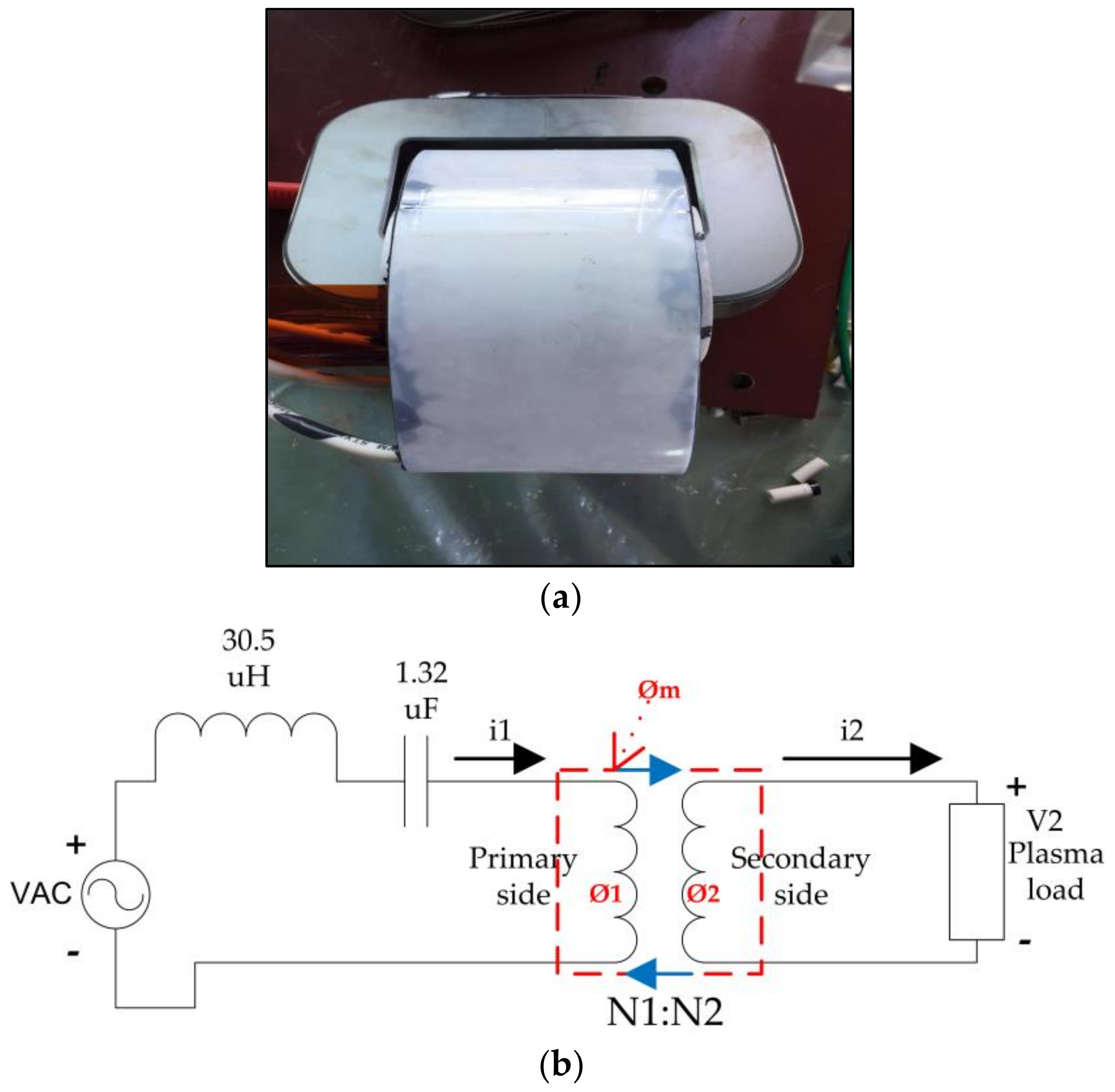
2.3. High Voltage High Frequency Transformer
A high voltage high frequency step-up transformer [
40] was designed in the laboratory, as shown in
Figure 5. The transformer step-up the inverter output voltage to a 10 kV peak to peak voltage and achieve galvanic isolation. A 100 nf capacitor is connected as a high pass filter between the inverter output and the primary winding of the high voltage transformer. It obtains the sine wave current waveform from the square wave voltage. The secondary side of the transformer output was connected to a quartz tube (plasma source), which was made of metal and titanium. The three high voltage capacitors were connected in parallel as a DC link with a value of 2040 μF, 450 V.
The necessity of the transformer is mainly for a high voltage value at the secondary side, a specific shape for industrial applications. The high voltage high frequency transformer was designed for the plasma power supply, and has the following electrical specifications: output voltage Vout = 10 kV; output power Pout = 5 kW. As per design, high switching frequency will decrease the height and size of the transformer. However, further reduction by higher frequency switching cannot be achieved because of the insulation requirement. The natural resonant frequency of the high voltage transformer is also a restriction. Additionally, high frequency switching will require high driving power. As a compromise, fs = 25 kHz is selected as the switching frequency.
2.3.1. Turns Ratio
The DC link voltage is approximately 300 V DC, which is obtained by the rectifier. The output voltage is 10 kV. So the output–input ratio should be 33.33. Both the turn’s ratio of the transformer and plasma power supply contribute to the final voltage boost. Thus, in practice, the step-up coefficient of the plasma power supply is used as design margin and the turn’s ratio of the high voltage transformer is selected as 33.33.
2.3.2. Magnetic Selection
Power ferrites are employed as the magnetic material due to the high resistivity and low eddy current losses under high frequency. PL-13, UU120 is designated to accommodate the big winding turns and to fulfill the insulation requirement.
The turn’s number of the primary and the secondary side winding, n1 and n2, can be calculated by (11) and (12), respectively, which yields n1 = 23, n2 = 770.
2.3.3. Wire and Wiring Design
The secondary winding plays a main role in the output voltage side. In practice, the secondary winding is wounded into five slots, each slot contains five layers. This assembly can limit the voltage across each slot and decrease the layer-to-layer voltage. Primary side used Ritz wire and secondary side high voltage Copper wire is used and results in a small leakage inductance. Considering the skin effect and the current value, the wire specifications and the current density are as follows: primary winding—0.2 mm Ritz wire, 3 A/mm2; Secondary winding—AWG16 high voltage cable copper wire, 1 A/mm2.
Primary and secondary windings have resistances, which means that the source voltage VAC is not the same as the induced primary voltage e
1; that is, VAC ≠ e
1. Similarly, V
2 ≠ e
2. The source voltage of primary side of transformer is coming from inverter output side. In deriving the equivalent circuit for the two-winding transformer of
Figure 5b, the characteristics of an actual transformer described earlier need to be modeled.
Consider the primary circuit. A voltage equation around the loop may be written as
where
2.4. Advantages and Disadvantages of the Circuit
Advantages:
- ➢
The power supply circuit has a smaller size.
- ➢
It is lightweight.
- ➢
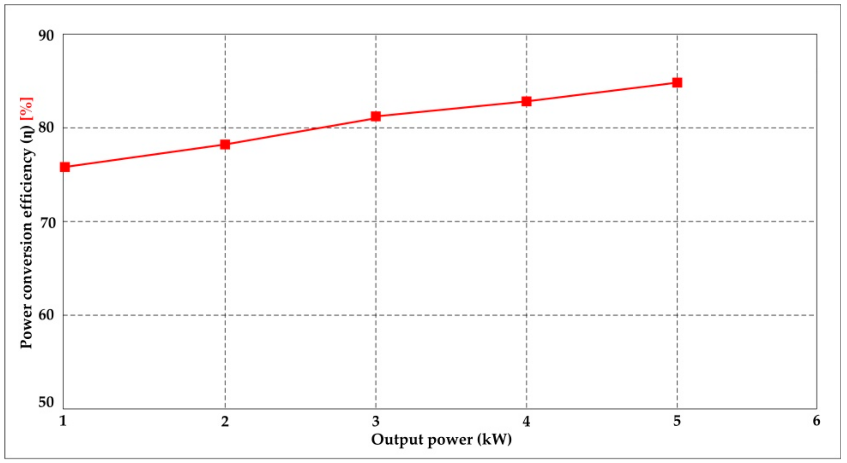
It has excellent power conversion efficiency from 75% to 85%.
- ➢
This design has high output range.
- ➢
Less heat produced in plasma power supply design.
- ➢
Simple application.
Disadvantages:
- ➢
This design has only one output range.
- ➢
It causes harmonic distortion.
- ➢
High frequency noise.
- ➢
More complex.
5. Results and Discussion
The HVHF plasma switching power supply design and workings are discussed below based on the experimental results. The experiments are made by applying output voltage 10 kV peak to peak. To verify the circuit, the experiments were carried out with a variable AC voltage and different input power.
Figure 7 shows the shows the DC voltage converted from the single phase AC sine wave with different input power.
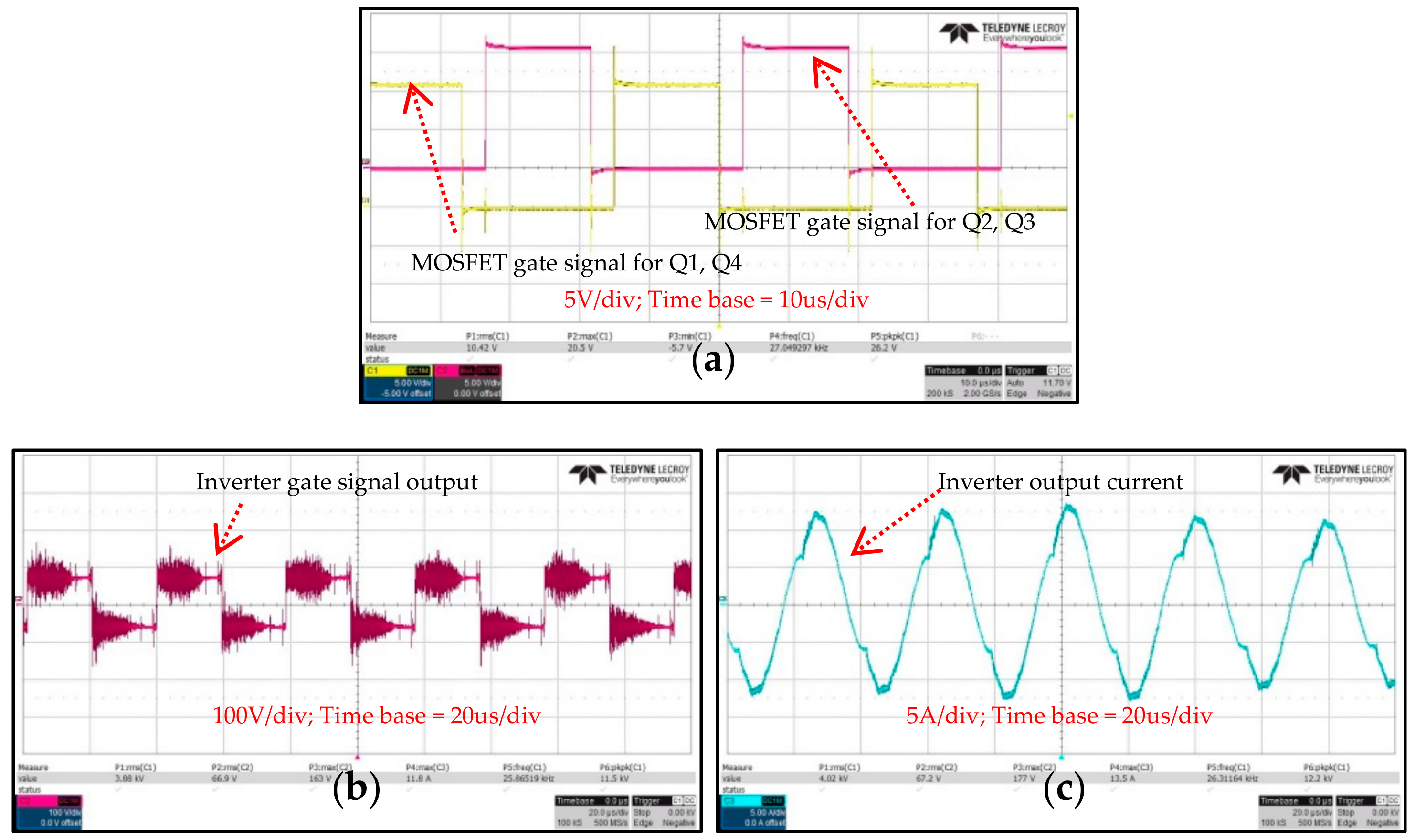
The high frequency PWM inverter output waveforms and gate signals are shown in
Figure 8. The inverter output and high frequency square wave voltages were obtained from the DC input voltage from the bridge rectifier circuit.
Figure 8a shows the two complementary 50% duty cycle PWM signals produced by the analog PWM controller. The two complementary PWM control signals synchronized with each other and consist of dead band, which avoids short circuit in full bridge. The controlled PWM signals were applied to the gate terminal of the MOSFET switches to switch the MOSFET on and off.
Figure 8b presents the output voltage of inverter waveforms at various input voltages and
Figure 8c presents output current waveform (5 A/div) of the inverter, respectively.
Figure 9 presents the HVHF plasma switching power supply output waveforms.
Figure 9a shows the output voltage waveform of the transformer secondary side with the 10 kV.
Figure 9b shows the output current waveform of inverter (5 A/div). The respective output current (500 mA/div) waveforms of the transformer secondary side that flow through the plasma source, as shown in
Figure 9c. The output current of the inverter side was changed to a sinewave because of the series connected filter.
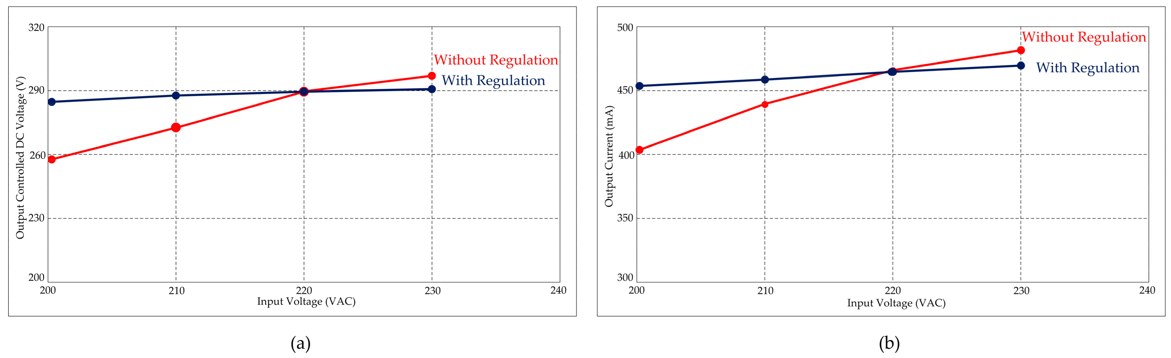
Figure 10 shows the HVHF plasma power supply characteristics waveforms with and without regulation.
Figure 10a presents the input voltage versus output DC controllable voltage and
Figure 10b exhibits the input voltage versus output current. This comparison graph results are reported with and without regulation. When different AC input voltages were applied (200 V AC to 230 V AC) to the proposed HVHF plasma power supply, the DC output voltage also varied from 259 V to 310 V. The large saturation in output voltage will affect the plasma source and lead to damage. Therefore, a line regulation circuit was designed to avoid this saturation in the output. The low cost line regulation achieved low output changes (282 V to 291 V) for the input voltage saturation from 200 V to 240 V, as shown in
Figure 10a. An output current of 407 mA to 484 mA was generated without regulation, whereas 455 mA to 472 mA was generated with regulation, as shown in
Figure 10b. Therefore, the proposed HVHF plasma power supply achieves a reliable output voltage and current for the plasma power source and assured safe operation.
Efficiency Optimization
Figure 11 shows the power conversion efficiency. The MOSFET switches are used for high repetition rates (25 kHz), and excellent output power conversion efficiency is achieved from 75% to 85%, as shown in
Figure 11. In order to examine the applied properties of the pulse generation arrangement, a set of prototypes was constructed. Basic experiments were plasma power supply design based on a topology depicted in
Figure 3a (As in manuscript). The power supplied with an initial voltage is 200 VAC to 240 VAC and the DC initial voltage is 300 V DC. Capacitors were implemented using high voltage type with the value of C1 = C2 = C3 = 680 μF each. The overall the output voltage of system is 10 kV
p-p. All the electrical waveforms were recorded using Teledyne Lecroy (350 MHz, 2 GS/s). Voltage pulse was measured by Teledyne Lecroy HighVoltage probe. Current was measured by a current monitor.
The capacitance is chosen at the outside side, namely C13 = 1.32 μF. The efficiency given below was calculated on the basis of energy balance of the DC link capacitors. This was measured using the half period voltage and current product.


