Pulsed Laser Deposition of Thin Films: Recent Advances and Challenges (Closed)

A topical collection in Coatings (ISSN 2079-6412). This collection belongs to the section "Laser Coatings".

Viewed by 34816

Editors


E-Mail Website
Guest Editor
Center for Advanced Laser Technologies (CETAL), National Institute for Laser, Plasma and Radiation Physics (INFLPR), 077125 Măgurele, Romania
Interests: laser processing of biomaterials; surface nanostructuring; biomimetic materials; tissue engineering; laser synthesis of bioactive coatings; biointerfaces; microfluidic platforms; lab-on-a-chip devices; 3D bioprinting

E-Mail Website
Guest Editor
Lasers Department, National Institute for Lasers, 409A Atomistilor street, 077125 Magurele, Ilfov, Romania
Interests: biomaterials; nanostructures and pharmacophores; laser applications in nanostructures for controlled drug administration; implants and tissue engineering
Special Issues, Collections and Topics in MDPI journals

Topical Collection Information

Dear Colleagues,

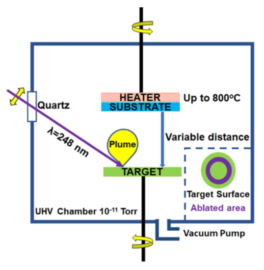
Since its first introduction several decades ago, Pulsed Laser Deposition (PLD), proved a powerful technique for the synthesis of a broad spectrum of functional thin films. Indeed, with respect to other conventional physical vapor deposition techniques, PLD exhibits several advantages, such as control of stoichiometry especially for materials with complex composition, adherent coatings, easy to obtain multi-layered thin films and combinatorial maps, good versatility of experimental design, and morphology and crystallinity control, to mention a few. Moreover, tailoring the composition-structure-properties relationship of the coatings is possible by adjusting the deposition conditions.

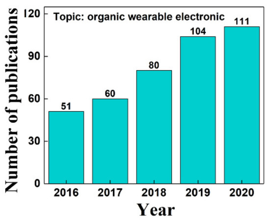
Matrix-assisted pulsed laser evaporation (MAPLE) is a complementary deposition technique derived from PLD, extensively explored for the deposition of thin organic nanoparticle and composite coatings. High experimental versatility allows synthesis of delicate compounds such as proteins or polymers, without impeding the stability of their functional characteristics. Although initially designed for polymers, MAPLE evolved into various applications in biomimetic coatings, energy, sensing, wearable electronics, and photonic devices.

In view of creating a knowledge platform devoted to laser-based deposition technologies, we kindly invite you to submit your recent work to our Special Issue entitled “Pulsed Laser Deposition of Thin Films: Recent Advances and Challenges.”

This Special Issue is devoted to recent advances and further challenges of PLD and its derivate MAPLE techniques applied but not limited to:

  • Biomimetic coatings (bioactive Calcium Phosphates, bio-glasses, biopolymers, and drug delivery systems)
  • Sensors and biosensors
  • Oxides and Transparent Conductive Oxides (TCO)
  • Organic and inorganic solar cells layers and multilayers
  • Smart windows and efficient energy coatings
  • Catalysts and energy storage devices
  • Hard carbides, nitrides and carbo-nitrides coatings
  • Coatings for extreme enviroments
  • Novel composites thin-films synthesis via material blending or multilayer assembling
  • Modelling and/or theoretical studies devoted to laser-matter interactions and thin films growth leading to innovative functionalities

Dr. Emanuel Axente
Dr. Gabriel Socol
Guest Editors

Manuscript Submission Information

Manuscripts should be submitted online at www.mdpi.com by registering and logging in to this website. Once you are registered, click here to go to the submission form. Manuscripts can be submitted until the deadline. All submissions that pass pre-check are peer-reviewed. Accepted papers will be published continuously in the journal (as soon as accepted) and will be listed together on the collection website. Research articles, review articles as well as short communications are invited. For planned papers, a title and short abstract (about 100 words) can be sent to the Editorial Office for announcement on this website.

Submitted manuscripts should not have been published previously, nor be under consideration for publication elsewhere (except conference proceedings papers). All manuscripts are thoroughly refereed through a single-blind peer-review process. A guide for authors and other relevant information for submission of manuscripts is available on the Instructions for Authors page. Coatings is an international peer-reviewed open access monthly journal published by MDPI.

Please visit the Instructions for Authors page before submitting a manuscript. The Article Processing Charge (APC) for publication in this open access journal is 2600 CHF (Swiss Francs). Submitted papers should be well formatted and use good English. Authors may use MDPI's English editing service prior to publication or during author revisions.

Keywords

  • laser-matter interactions
  • biomimetic coatings
  • organic, inorganic and hybrid thin films
  • pulsed laser deposition (PLD)
  • matrix assisted pulsed laser evaporation (MAPLE)
  • combinatorial laser technologies
  • surface micro-processing
  • tissue engineering
  • drug delivery
  • sensors
  • solar cells

Published Papers (9 papers)

2022

Jump to: 2021, 2020

13 pages, 2847 KiB  
Article
Thin Film Fabrication by Pulsed Laser Deposition from TiO2 Targets in O2, N2, He, or Ar for Dye-Sensitized Solar Cells
by Dorel F. Albu, Jeanina Lungu, Gianina Popescu-Pelin, Cristian N. Mihăilescu, Gabriel Socol, Adrian Georgescu, Marcela Socol, Alexandra Bănică, Victor Ciupina and Ion N. Mihailescu
Coatings 2022, 12(3), 293; https://doi.org/10.3390/coatings12030293 - 22 Feb 2022
Cited by 10 | Viewed by 3183
Abstract
Active semiconductor layers of TiO2 were synthesized via pulsed laser deposition in He, N2, O2, or Ar to manufacture DSSC structures. As-prepared nanostructured TiO2 coatings grown on FTO were photosensitized by the natural absorption of the N719 [...] Read more.
Active semiconductor layers of TiO2 were synthesized via pulsed laser deposition in He, N2, O2, or Ar to manufacture DSSC structures. As-prepared nanostructured TiO2 coatings grown on FTO were photosensitized by the natural absorption of the N719 (Ruthenium 535-bis TBA) dye to fabricate photovoltaic structures. TiO2 photoanode nanostructures with increased adsorption areas of the photosensitizer (a combination with voluminous media) were grown under different deposition conditions. Systematic SEM, AFM, and XRD investigations were carried out to study the morphological and structural characteristics of the TiO2 nanostructures. It was shown that the gas nature acts as a key parameter of the architecture and the overall performance of the deposited films. The best electro-optical performance was reached for photovoltaic structures based on TiO2 coatings grown in He, as was demonstrated by the short-circuit current (Isc) of 5.40 mA, which corresponds to the higher recorded roughness (of 44 ± 2.9 nm RMS). The higher roughness is thus reflected in a more efficient and deeper penetration of the dye inside the nanostructured TiO2 coatings. The photovoltaic conversion efficiency (η) was 1.18 and 2.32% for the DSSCs when the TiO2 coatings were deposited in O2 and He, respectively. The results point to a direct correlation between the electro-optical performance of the prepared PV cells, the morphology of the TiO2 deposited layers, and the crystallinity features, respectively. Full article
Show Figures

Figure 1

2021

Jump to: 2022, 2020

32 pages, 43213 KiB  
Review
Organic Thin Films Deposited by Matrix-Assisted Pulsed Laser Evaporation (MAPLE) for Photovoltaic Cell Applications: A Review
by Marcela Socol, Nicoleta Preda and Gabriel Socol
Coatings 2021, 11(11), 1368; https://doi.org/10.3390/coatings11111368 - 8 Nov 2021
Cited by 10 | Viewed by 2999
Abstract
Human society’s demand for energy has increased faster in the last few decades due to the world’s population growth and economy development. Solar power can be a part of a sustainable solution to this world’s energy need, taking into account that the cost [...] Read more.
Human society’s demand for energy has increased faster in the last few decades due to the world’s population growth and economy development. Solar power can be a part of a sustainable solution to this world’s energy need, taking into account that the cost of the renewable energy recently dropped owed to the remarkable progress achieved in the solar panels field. Thus, this inexhaustible source of energy can produce cheap and clean energy with a beneficial impact on the climate change. The considerable potential of the organic photovoltaic (OPV) cells was recently emphasized, with efficiencies exceeding 18% being achieved for OPV devices with various architectures. The challenges regarding the improvement in the OPV performance consist of the selection of the adequate raw organic compounds and manufacturing techniques, both strongly influencing the electrical parameters of the fabricated OPV devices. At the laboratory level, the solution-based techniques are used in the preparation of the active films based on polymers, while the vacuum evaporation is usually involved in the deposition of small molecule organic compounds. The major breakthrough in the OPV field was the implementation of the bulk heterojunction concept but the deposition of mixed films from the same solvent is not always possible. Therefore, this review provides a survey on the development attained in the deposition of organic layers based on small molecules compounds, oligomers and polymers using matrix-assisted pulsed laser evaporation (MAPLE)-based deposition techniques (MAPLE, RIR-MAPLE and emulsion-based RIR-MAPLE). An overview of the influence of various experimental parameters involved in these laser deposition methods on the properties of the fabricated layers is given in order to identify, in the forthcoming years, new strategies for enhancing the OPV cells performance. Full article
Show Figures

Figure 1

14 pages, 44652 KiB  
Article
Surface Topography of Si/TiO2 Stacked Layers on Silicon Substrate Deposited by KrF Excimer Laser Ablation
by Călin Constantin Moise, Aida Pantazi, Geanina Valentina Mihai, Alin Jderu, Mircea Bercu, Angelo Alberto Messina and Marius Enăchescu
Coatings 2021, 11(11), 1350; https://doi.org/10.3390/coatings11111350 - 2 Nov 2021
Cited by 1 | Viewed by 2070
Abstract
This study investigates the surface topography of the deposited thin films versus the distance between target and substrate (dTS) inside a laser ablation equipment. The profile of the rough surface was obtained by atomic force microscopy data analysis based on [...] Read more.
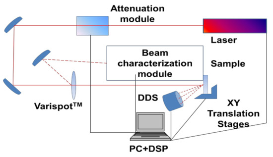
This study investigates the surface topography of the deposited thin films versus the distance between target and substrate (dTS) inside a laser ablation equipment. The profile of the rough surface was obtained by atomic force microscopy data analysis based on power spectral density and the roughness-length scale (RLS) functions. The roughing on the top film is analyzed considering the previous topography of the underneath surface for each consecutive TiO2 and Si deposition onto Si (100) wafer. The buried oxide layer inside of Si/TiO2/c-Si structure, obtained by KrF excimer laser ablation was characterized by complementary techniques as spectral ellipsometry, X-ray reflectometry, and X-ray diffraction. Full article
Show Figures

Figure 1

17 pages, 3105 KiB  
Review
Langmuir Probe Technique for Plasma Characterization during Pulsed Laser Deposition Process
by Stefan Andrei Irimiciuc, Sergii Chertopalov, Jan Lancok and Valentin Craciun
Coatings 2021, 11(7), 762; https://doi.org/10.3390/coatings11070762 - 25 Jun 2021
Cited by 32 | Viewed by 5191
Abstract
The history of pulsed laser deposition (PLD) and transient plasmas generated by laser ablation is intertwined with the development of various techniques for its fundamental understanding. Some diagnostic tools have been developed to better suit the rapid transient nature of the plasma (space [...] Read more.
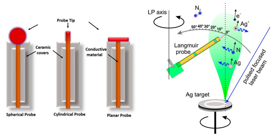
The history of pulsed laser deposition (PLD) and transient plasmas generated by laser ablation is intertwined with the development of various techniques for its fundamental understanding. Some diagnostic tools have been developed to better suit the rapid transient nature of the plasma (space and time dependence of all parameters, fast decay and complex chemistry inside the plasma), whereas others have been adapted from basic plasma physics studies. Langmuir probe method has been used as a real-time in situ diagnostic tool for laser ablation and later for PLD. It remains a useful tool for the PLD community arsenal, which can easily be adapted to the development of new lasers and ablation regimes and new deposition configuration, being one of the most versatile techniques for plasma diagnostics. It is the cornerstone on which charge particles are analyzed and has led to several important discoveries, such as multiple peak distribution, selective acceleration during expansion, plume splitting, plasma turbulences and fluctuations. However, because the Langmuir probe theory adaptation from classical plasma physics is not straightforward, it might lead to misinterpretation and often incorrect analysis of data. This review analyzes the limits and understanding of the technique as a foundation for attaining its full potential, which can impact the way PLD is used. This is especially useful for the pressing need of real-time, in-situ diagnostics and feedback loops for systematic semi-industrial implementation of the PLD technique. Full article
Show Figures

Figure 1

12 pages, 35023 KiB  
Article
Properties of Hafnium and Aluminium Silicates Coatings Obtained by PLD
by Eduard N. Sirjita, Laurentiu Rusen, Simona Brajnicov, Cristina Craciun, Valentin Ion, Mihaela Filipescu and Maria Dinescu
Coatings 2021, 11(7), 753; https://doi.org/10.3390/coatings11070753 - 23 Jun 2021
Cited by 5 | Viewed by 2980
Abstract
We report on the deposition and characterization of hafnium silicate and aluminium silicate thin films for different applications in optics and electronics. Pulsed laser deposition in a controllable oxygen atmosphere was used as a processing technique, with optimized parameters in terms of laser [...] Read more.
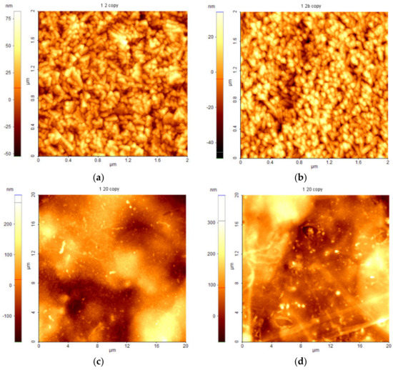
We report on the deposition and characterization of hafnium silicate and aluminium silicate thin films for different applications in optics and electronics. Pulsed laser deposition in a controllable oxygen atmosphere was used as a processing technique, with optimized parameters in terms of laser wavelength, laser fluence and oxygen pressure. The thin films were investigated using atomic force microscopy, spectroscopic ellipsometry, UV–VIS spectroscopy and X-ray photoelectron spectroscopy. The morphological investigations evidenced uniform layers with low roughness (in the order of nanometres). The optical investigations revealed that aluminium silicate layers with low roughness and low absorption in the infrared (IR) range can be obtained at high substrate temperatures (600 °C). The behaviour of the silicate thin films with respect to the nanosecond IR laser irradiation revealed that aluminium silicate layers have higher laser-induced damage threshold values in comparison with hafnium silicate. Full article
Show Figures

Figure 1

23 pages, 44474 KiB  
Review
Laser Coatings via State-of-the-Art Additive Manufacturing: A Review
by Muhammad Arif Mahmood, Alexandra Bănică, Carmen Ristoscu, Nicu Becherescu and Ion N. Mihăilescu
Coatings 2021, 11(3), 296; https://doi.org/10.3390/coatings11030296 - 4 Mar 2021
Cited by 22 | Viewed by 5656
Abstract
Ceramics and ceramic-reinforced metal matrix composites (CMMCs) demonstrate high wear resistance, excellent chemical inertness, and exceptional properties at elevated temperatures. These characteristics are suitable for their utilization in biomedical, aerospace, electronics, and other high-end engineering industries. The aforementioned performances make them difficult to [...] Read more.
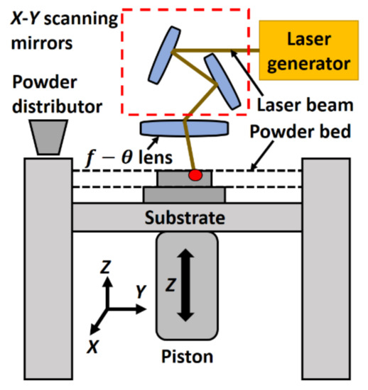
Ceramics and ceramic-reinforced metal matrix composites (CMMCs) demonstrate high wear resistance, excellent chemical inertness, and exceptional properties at elevated temperatures. These characteristics are suitable for their utilization in biomedical, aerospace, electronics, and other high-end engineering industries. The aforementioned performances make them difficult to fabricate via conventional manufacturing methods, requiring high costs and energy consumption. To overcome these issues, laser additive manufacturing (LAM) techniques, with high-power laser beams, were developed and extensively employed for processing ceramics and ceramic-reinforced CMMCs-based coatings. In respect to other LAM processes, laser melting deposition (LMD) excels in several aspects, such as high coating efficiency and lower labor cost. Nevertheless, difficulties such as poor bonding between coating and substrate, cracking, and reduced toughness are still encountered in some LMD coatings. In this article, we review recent developments in the LMD of ceramics and CMMCs-based coatings. Issues and solutions, along with development trends, are discussed and summarized in support of implementing this technology for current industrial use. Full article
Show Figures

Figure 1

10 pages, 3325 KiB  
Article
Direct-ARPES and STM Investigation of FeSe Thin Film Growth by Nd:YAG Laser
by Sandeep Kumar Chaluvadi, Debashis Mondal, Chiara Bigi, Jun Fujii, Rajdeep Adhikari, Regina Ciancio, Alberta Bonanni, Giancarlo Panaccione, Giorgio Rossi, Ivana Vobornik and Pasquale Orgiani
Coatings 2021, 11(3), 276; https://doi.org/10.3390/coatings11030276 - 26 Feb 2021
Cited by 6 | Viewed by 5040
Abstract
Research on ultrathin quantum materials requires full control of the growth and surface quality of the specimens in order to perform experiments on their atomic structure and electron states leading to ultimate analysis of their intrinsic properties. We report results on epitaxial FeSe [...] Read more.
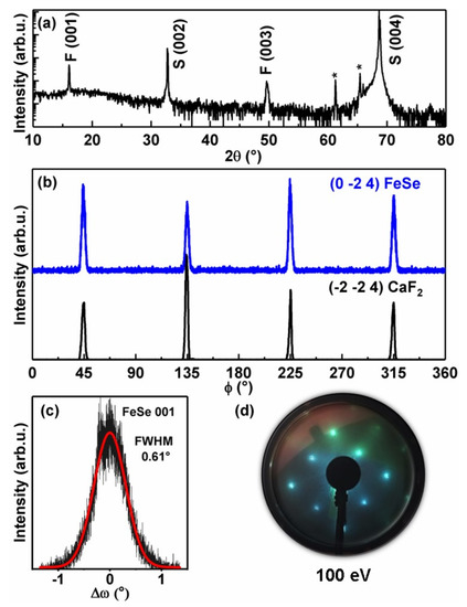
Research on ultrathin quantum materials requires full control of the growth and surface quality of the specimens in order to perform experiments on their atomic structure and electron states leading to ultimate analysis of their intrinsic properties. We report results on epitaxial FeSe thin films grown by pulsed laser deposition (PLD) on CaF2 (001) substrates as obtained by exploiting the advantages of an all-in-situ ultra-high vacuum (UHV) laboratory allowing for direct high-resolution surface analysis by scanning tunnelling microscopy (STM), synchrotron radiation X-ray photoelectron spectroscopy (XPS) and angle-resolved photoemission spectroscopy (ARPES) on fresh surfaces. FeSe PLD growth protocols were fine-tuned by optimizing target-to-substrate distance d and ablation frequency, atomically flat terraces with unit-cell step heights are obtained, overcoming the spiral morphology often observed by others. In-situ ARPES with linearly polarized horizontal and vertical radiation shows hole-like and electron-like pockets at the Γ and M points of the Fermi surface, consistent with previous observations on cleaved single crystal surfaces. The control achieved in growing quantum materials with volatile elements such as Se by in-situ PLD makes it possible to address the fine analysis of the surfaces by in-situ ARPES and XPS. The study opens wide avenues for the PLD based heterostructures as work-bench for the understanding of proximity-driven effects and for the development of prospective devices based on combinations of quantum materials. Full article
Show Figures

Figure 1

2020

Jump to: 2022, 2021

12 pages, 4281 KiB  
Article
Piezoelectric Hybrid Heterostructures PVDF/(Ba,Ca)(Zr,Ti)O3 Obtained by Laser Techniques
by Nicoleta Enea, Valentin Ion, Antoniu Moldovan, Anca Bonciu and Nicu Doinel Scarisoreanu
Coatings 2020, 10(12), 1155; https://doi.org/10.3390/coatings10121155 - 26 Nov 2020
Cited by 2 | Viewed by 2629
Abstract
In this paper we report the development of thin films composed of two piezoelectric materials, namely (Ba(Ti0.8Zr0.2)O3-x(Ba0.7Ca0.3)TiO3 (BCTZ) and polyvinylidene difluoride (PVDF), thus obtaining high piezoelectric hybrid heterostructures for making [...] Read more.
In this paper we report the development of thin films composed of two piezoelectric materials, namely (Ba(Ti0.8Zr0.2)O3-x(Ba0.7Ca0.3)TiO3 (BCTZ) and polyvinylidene difluoride (PVDF), thus obtaining high piezoelectric hybrid heterostructures for making them a viable option for wearable pressure sensors. The piezoelectric output response as a function of different weight percentage of BCTZ ceramic powders (x = 0.50 BCTZ50 and x = 0.55 BCTZ55) in the PVDF matrix was investigated. The highest value of the piezoelectric coefficient d33 and the capacitance, with low dielectric loss was obtained for the heterostructure composed of PVDF/BCTZ50. Full article
Show Figures

Figure 1

12 pages, 3839 KiB  
Article
MAPLE Deposition of Binary and Ternary Organic Bulk Heterojunctions Based on Zinc Phthalocyanine
by Marcela Socol, Nicoleta Preda, Gabriela Petre, Andreea Costas, Oana Rasoga, Gianina Popescu-Pelin, Andreea Mihailescu, Anca Stanculescu and Gabriel Socol
Coatings 2020, 10(10), 956; https://doi.org/10.3390/coatings10100956 - 4 Oct 2020
Cited by 5 | Viewed by 2324
Abstract
Organic bulk heterojunctions (BHJ) based on zinc phthalocyanine (ZnPc), fullerene compounds (C60 fullerene and [6,6]-phenyl C71 butyric acid methyl ester (PC70BM)), and 5,6,11,12-tetraphenylnaphthacene (rubrene) were fabricated through the matrix-assisted pulsed-laser evaporation (MAPLE) technique. Thus, ZnPc:C60 and ZnPc:PC70BM binary BHJ and ZnPc:rubrene:PC70BM ternary BHJ [...] Read more.
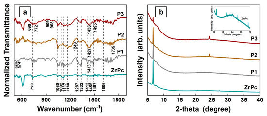
Organic bulk heterojunctions (BHJ) based on zinc phthalocyanine (ZnPc), fullerene compounds (C60 fullerene and [6,6]-phenyl C71 butyric acid methyl ester (PC70BM)), and 5,6,11,12-tetraphenylnaphthacene (rubrene) were fabricated through the matrix-assisted pulsed-laser evaporation (MAPLE) technique. Thus, ZnPc:C60 and ZnPc:PC70BM binary BHJ and ZnPc:rubrene:PC70BM ternary BHJ were deposited as thin films on various substrates. The preservation of the chemical structure of the organic compounds during the MAPLE deposition was confirmed by infrared spectroscopy. The structural, optical, and morphological properties of the deposited layers were investigated by X-ray diffraction (XRD), UV-Vis spectroscopy, photoluminescence (PL), field emission scanning electron microscopy (FESEM), and atomic force microscopy (AFM), respectively. Further, the electrical properties of the developed structures based on ZnPc:C60, ZnPc:PC70BM, and ZnPc:rubrene:PC70BM were evaluated. The J-V characteristics of the organic structures, recorded under illumination, show that an increase in the open-circuit voltage (VOC) is achieved in the case of the ternary blend in comparison with that obtained for the binary blends. The results evidenced that MAPLE-deposited thin films containing binary and ternary organic bulk heterojunctions can find applications in the field of photovoltaic devices. Full article
Show Figures

Figure 1

Back to TopTop