1. Introduction
Renewable energy resources are becoming popular and trendy with the increase in demand and cost of energy. The proper utilization of energy resources is one of the most important issues of the present century. There are various renewable energy resources, including solar, tidal, wind, bio, nuclear and geothermal, with zero pollution emissions. Solar energy is a free, inexhaustible source of energy and is increasingly competitive with other energy sources. This energy is utilized with the help of arrays, consisting of a number of solar panels, connected in series [
1,
2,
3]. In the past, various PV system methods or structures were adopted to minimize the cost to efficiency ratio. In [
4,
5,
6,
7,
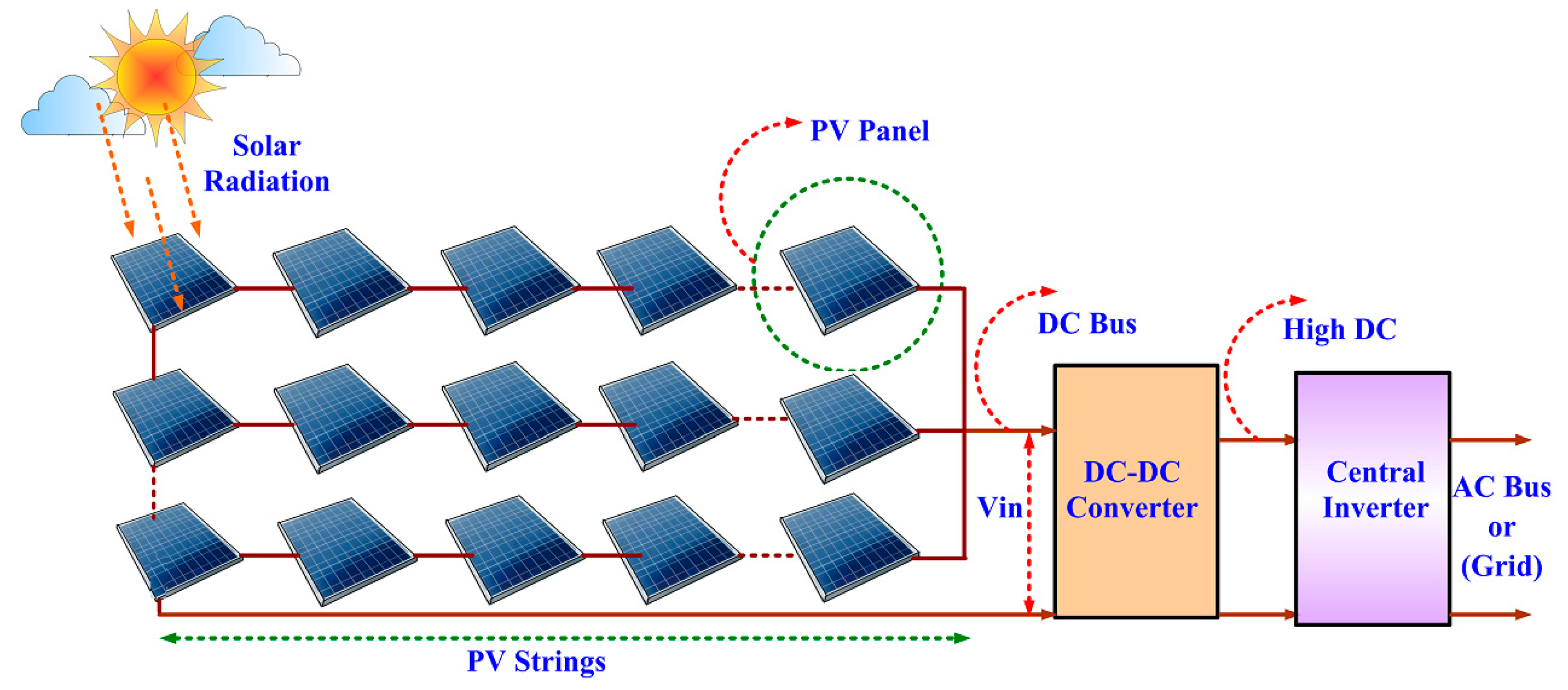
8], a Photovoltaic Central Inverter Structure (PV-CIS) is employed to feed photovoltaic energy to the electric grid. In PV-CIS PV lines are arranged in parallel and connected to one central inverter as shown in
Figure 1. The drawback of CIS are: (i) a large number of panels are required which increases the cost of system; (ii) more number of DC cables with high-voltage rating are needed; (iii) losses in the line; (iv) loss of power due to module mismatch; (v) common Maximum Power Point Tracking (MPPT) is used; (vi) system reliability depends on the single inverter.
In [
4,
5,
6,
7,
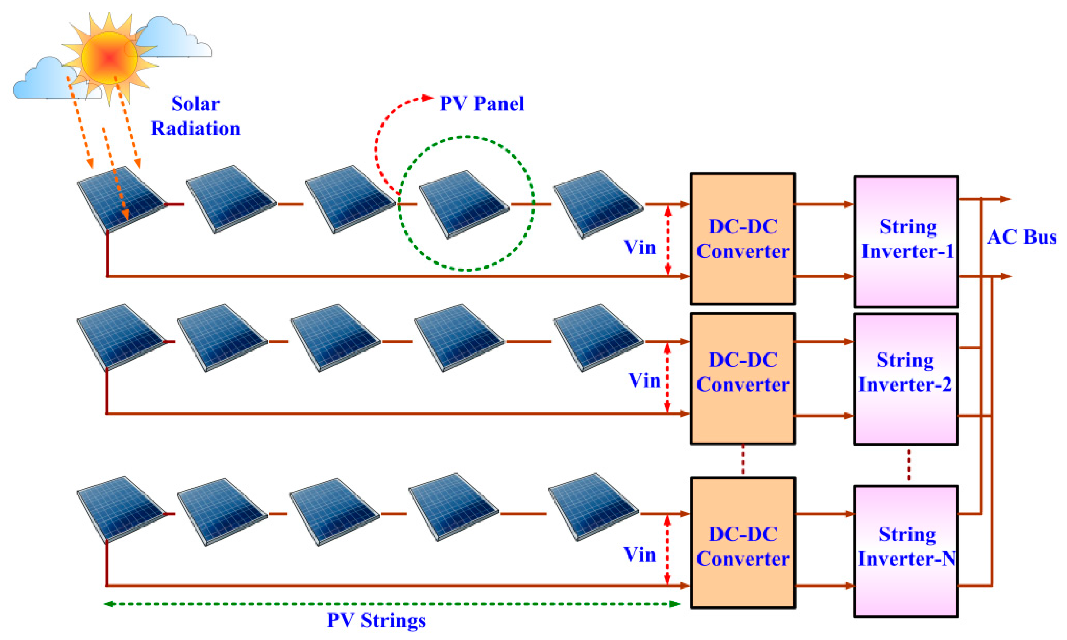
8], a Photovoltaic String Inverter structure (PV-SIS) is employed to feed photovoltaic energy to the electric grid. In PV-SIS, several PV lines are used, which are made up of several series- connected PV panels as shown in
Figure 2. All the PV lines are connected to separate inverters via a DC-DC converter and the inverter outputs are connected in parallel and feed into the electric grid. The drawbacks of the PV-SIS system are: (i) it requires a large number of panels to design a several PV line; (ii) a large number of converters are required to feed the grid; (iii) the cost is high due to the separate MPPT and complex control circuitry is required to synchronize all the inverters.
In [
4,
5,
6,
7,
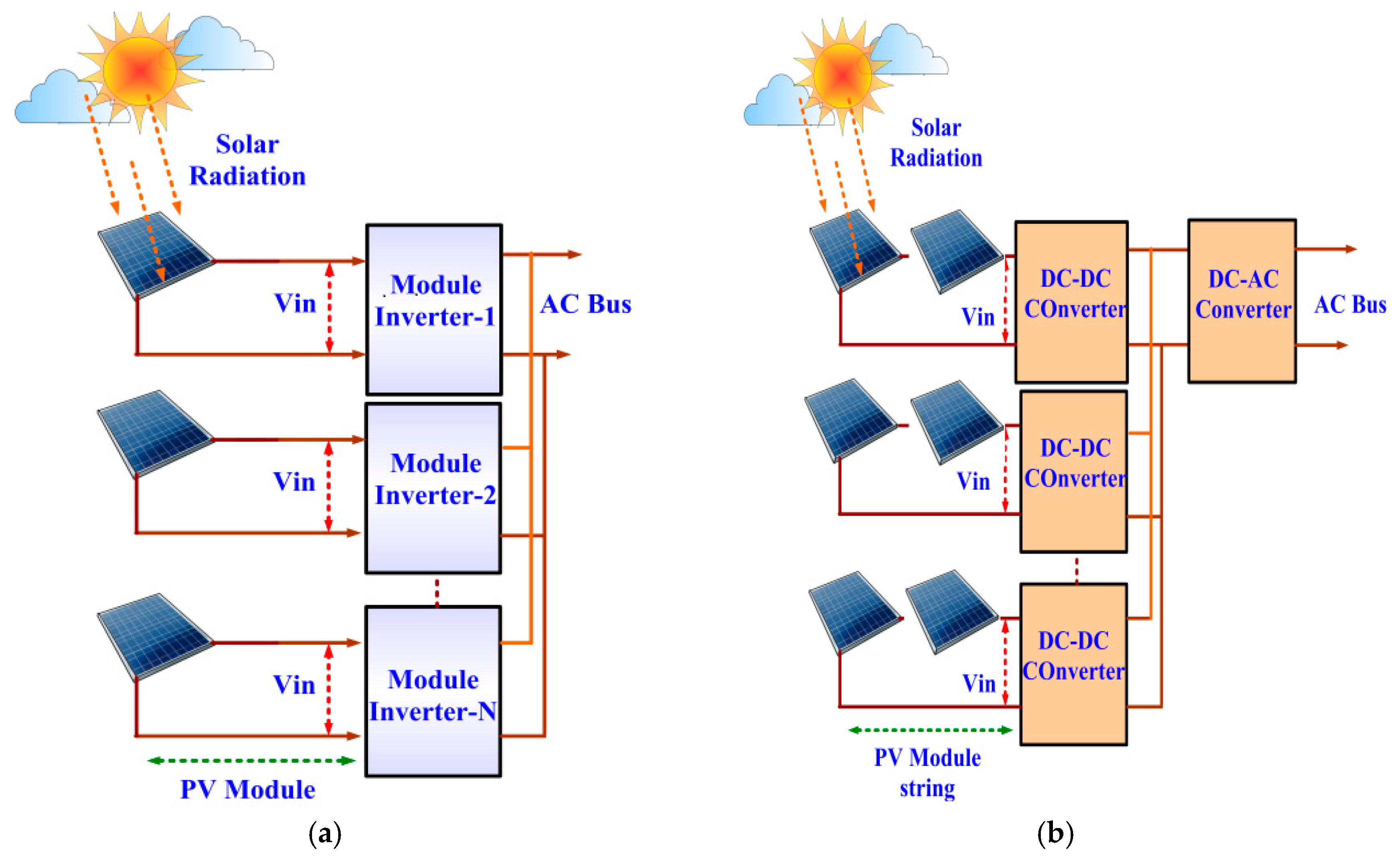
8], Photovoltaic AC Module Structure (PV-ACMS) is discussed to fed photovoltaic energy to the electric grid and it provides a viable solution to overcome the drawbacks of PV-CIS and PV-SIS. In PV-ACMS a single photovoltaic panel is connected to the electric grid via an inverter as shown in
Figure 3a. The drawbacks of PV-ACMS are: (i) it requires several module inverters which increase the cost of the system; (ii) separate MPPT is needed for each panel; (iii) the overall efficiency is low. In [
4,
5,
6,
7,
8], Photovoltaic Multi-String Inverter Structure (PV-MSIS) is discussed to overcome the drawback of PV-CIS, PV-SIS and PV-SIS structures. In PV-MSIS several PV panels are connected to a single inverter connected via several DC-DC converters as shown in
Figure 3b. This structure combines the features of PV-SIS and PV-ACMS. The drawback of the PV-MSIS concept is: (i) it required several DC-DC converters to transfer energy to the inverter; (ii) high cost due to the greater number of converters and separate MPPT.
The output obtained from a photovoltaic cell/array is usually low, so before feeding this voltage to the inverter for practical application purposes, it must be stepped up using a conventional DC-DC boost converter [
1,
2,
3,
4,
5,
6,
7,
8,
9,
10,
11,
12,
13,
14,
15]. With the increase in the duty-cycle of switch and leakage resistance of inductors, the performance of the converter degrades. Due to these practical problems, conventional DC-DC converters are unable to provide doable solutions for step-up voltage applications [
15]. In theory, when a duty cycle approaches 100%, an infinite voltage conversion ratio is achieved with a conventional boost converter, but in practice, the inductor leakage resistance of the inductor limits the voltage conversion of the converter [
16], so the traditional converters cannot be used where the required conversion ratio is four or more [
16]. Furthermore, to achieve a high conversion ratio by using large duty cycle compromises the utilization of high frequency for Pulse Width Modulation (PWM) because of semiconductor control devices’ inherent switching delay. Unluckily, a large reactive network follows the limited switching frequency which is employed to protect from the ripple condition of voltage and current [
17]. The traditional buck-boost converter is not reliable due to its discontinuous input current, which results in low utilization of the input source [
13,
15]. By increasing the switching frequency of the converter, the problem of leakage resistance for certain values of ripple can be overcome. The finite switching time in a normal power device limits the switching frequency if the duty ratio is either too high or too small, so in order to abolish the above problems and simultaneously acquire essential high voltage, isolated converters can be engaged. Many isolated and non-isolated converter topologies have proposed over time, which make use of inductors, coupled inductors and transformers [
16,
17,
18,
19,
20,
21,
22,
23,
24,
25,
26,
27]. The high voltage stress occurring due to the transformer leakage inductance leads to switching losses and electromagnetic interference (EMI) problems, resulting in the reduced efficiency of conventional converters. Hard switching converters are inconvenient to use for high voltage applications due to their circuit complexity, higher voltage stress across the switch and the increased cost of the converter. Hence, for isolated topologies the size, weight and losses of power transformers are limiting factors. Recently, various combinations of coupled inductors, voltage multipliers or switched capacitor multipliers [
23,
24,
25,
26,
27,
28,
29,
30,
31,
32,
33,
34,
35] along with a switched inductor (SI), switched capacitor (SC), voltage lift switched inductor (VLSI) and modified VLSI principles were used to accomplish the necessity [
15,
26].
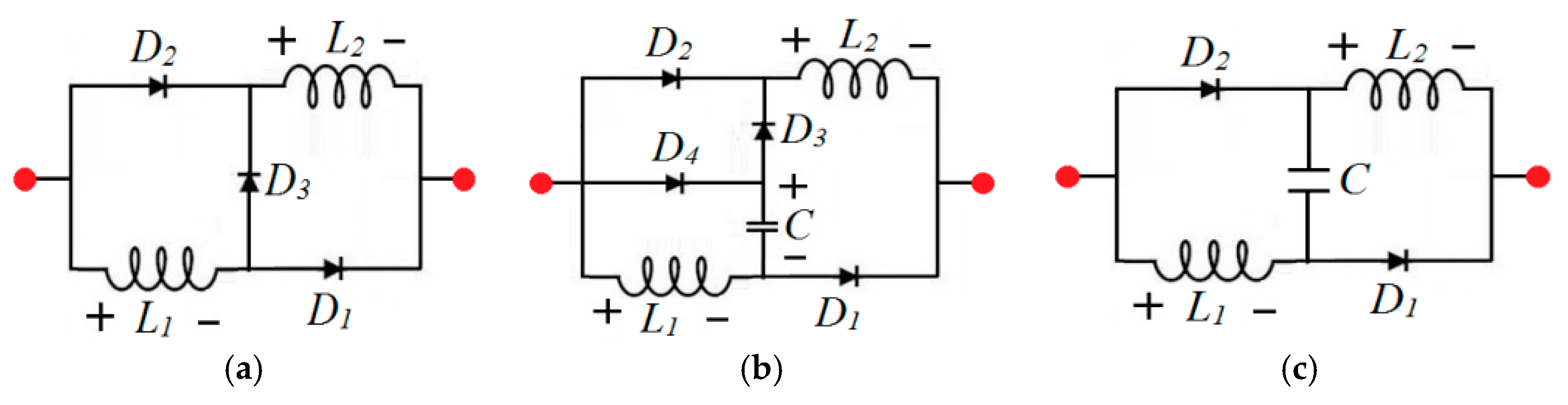
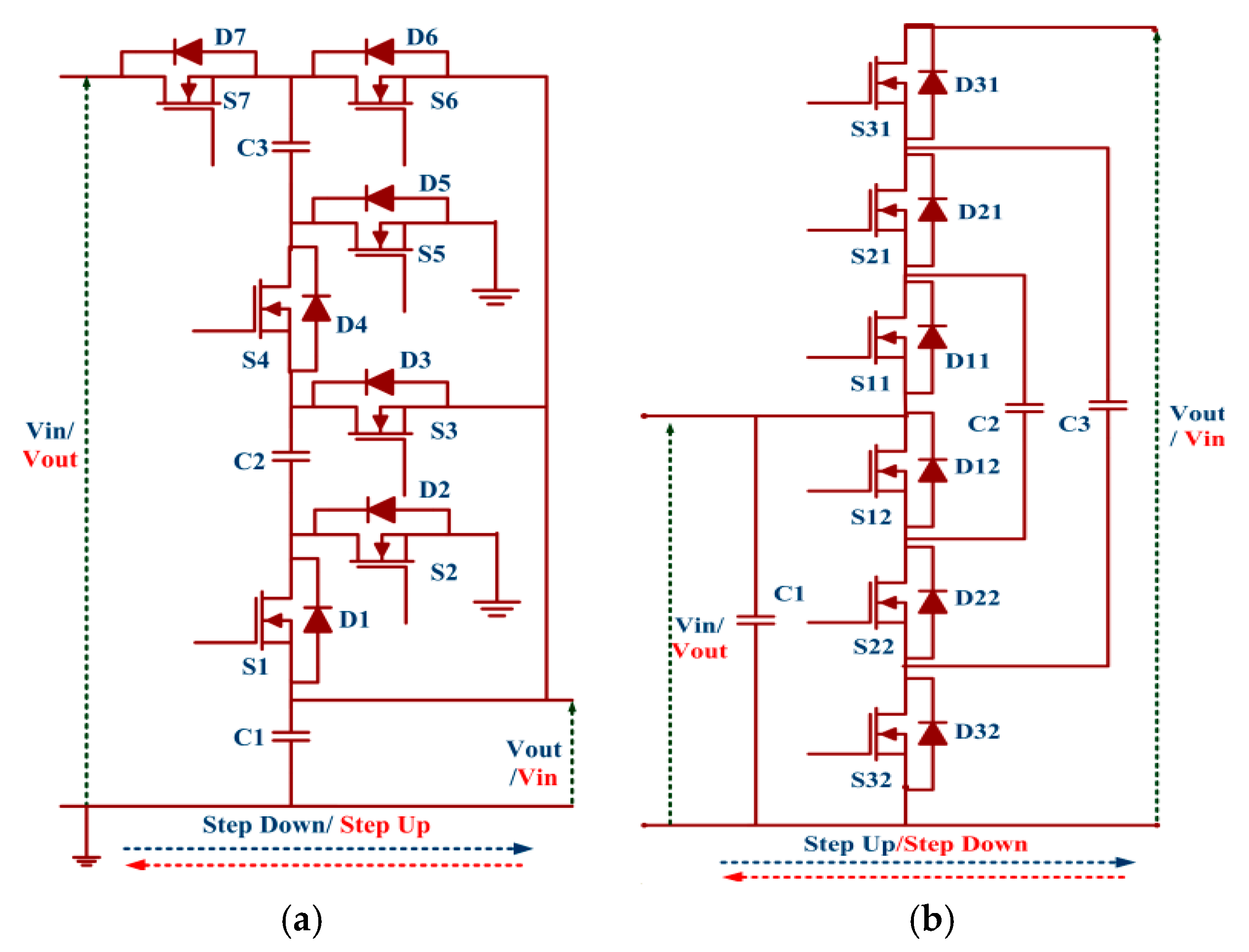
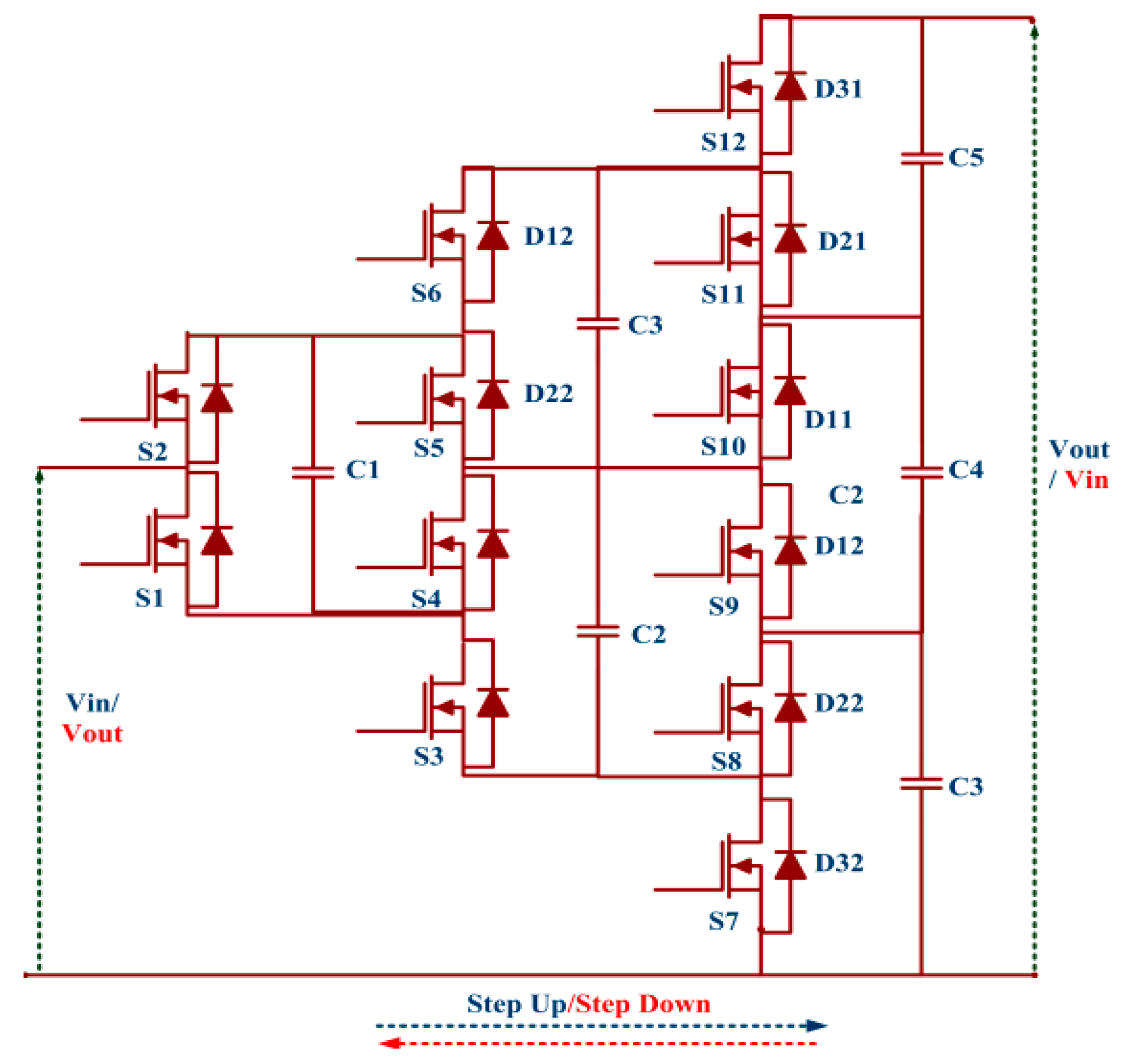
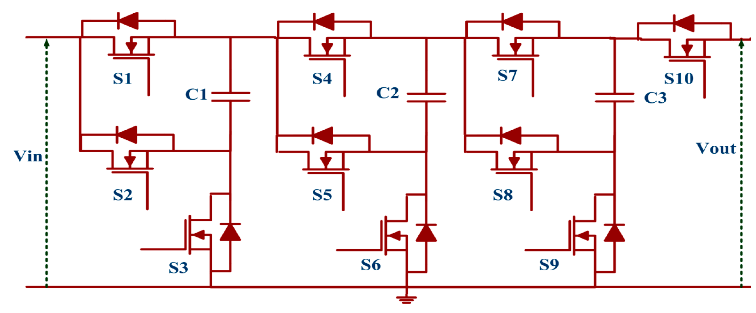
Figure 4a–c shows the recent SI, VLSI and modified VLSI inductive networks. For acquiring a high boost ratio, a cascaded approach is introduced. To design a Cascaded Boost Converter (CBC), a number of inductors are essential, which is the most complex part. In addition, losses and increased current ripple prove to be a barrier to achieve a high conversion ratio and better efficiency [
36,
37,
38]. With an objective of acquiring a high voltage gain just by using a single switch, the Quadratic Boost Converter (QBC) was proposed, though, in a QBC, higher voltage rating switches are required with higher R
DS-ON, as voltage stress raised across the switch is equal to the output voltage [
39,
40,
41]. Multilevel converters provide a suitable solution for power conversion because of the low voltage stress across each device [
42]. High voltage is achieved by multilevel DC-DC converters using capacitors and diode circuitry at the output end and the output voltage level can be increased without actually disturbing the actual circuit. By varying the number of output levels and duty cycle, the voltage gain of multilevel converters can be varied [
43,
44]. For conventional multilevel converters, designing magnetic components like inductors is a complex task, which also induces electromagnetic emission noise. Other than these issues the presence of inductors and transformers in the power circuit degrades the integration capability and increases the cost, weight and size of the converters. Switched Capacitor (SC) power circuits provide good integration ability due to their small volume and weight, since magnetic components like transformers and inductors is not needed to design a SC converter [
33].
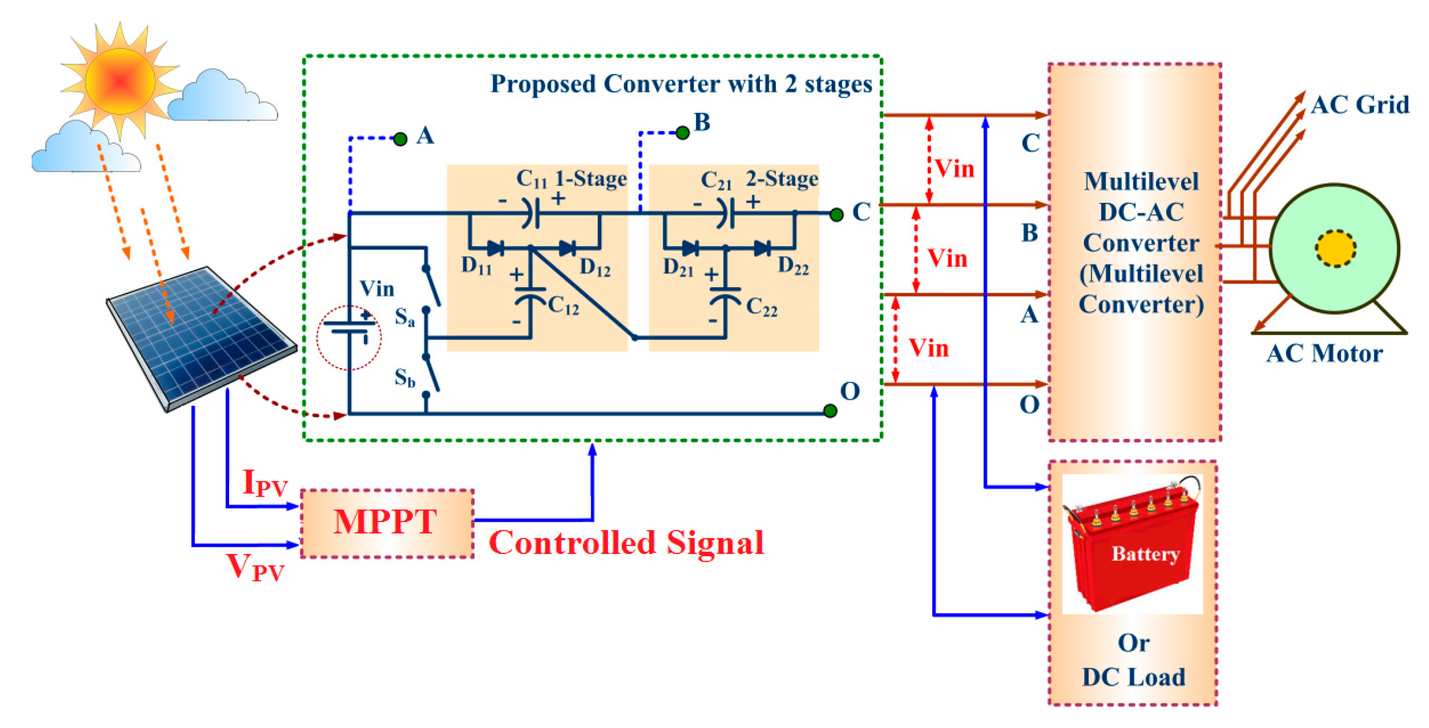
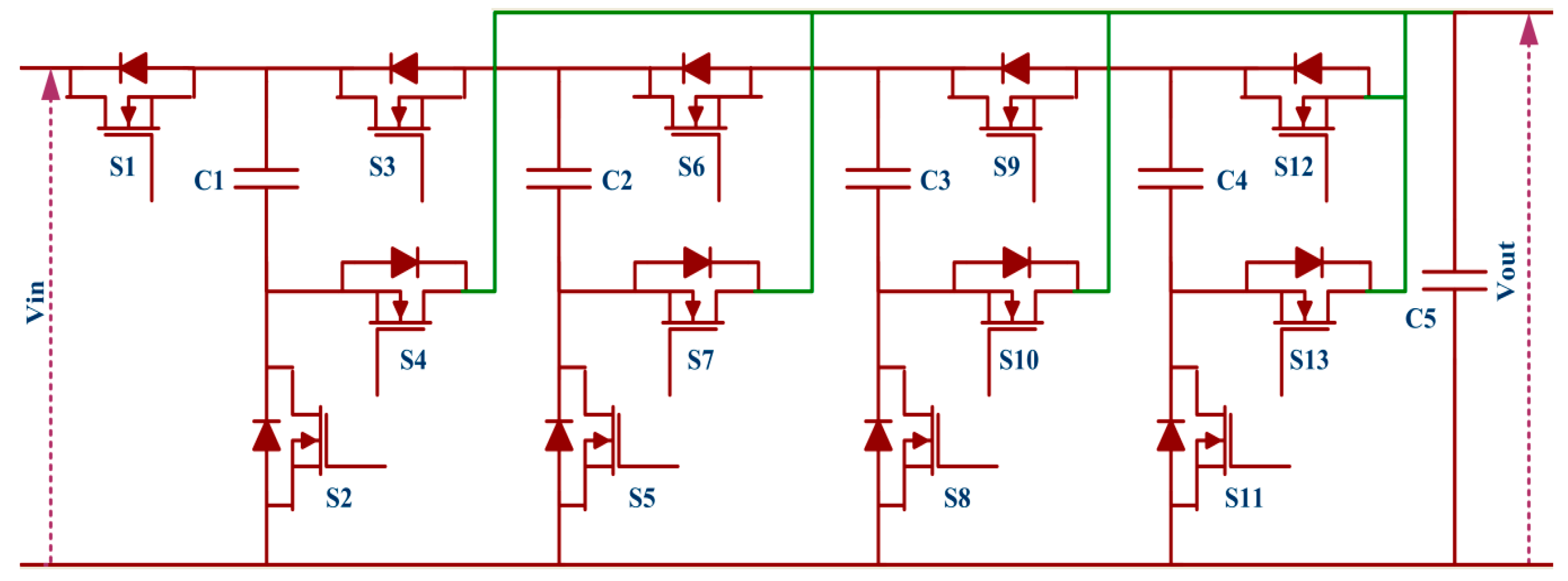
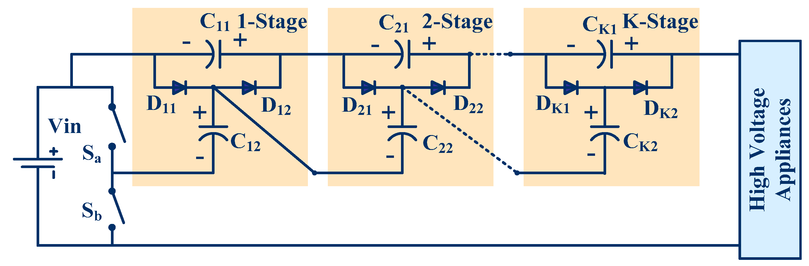
In this article, a new magnetic component-free (transformer-less and inductor-less) DC-DC converter is proposed to overcome the drawbacks of PV-CIS, PV-SIS, PV-ACMS, PV-MSIS and the above discussed converter topology. The proposed converter provides a viable solution for existing photovoltaic application systems where voltage must be stepped up without magnetic components before transferring energy to a multilevel-inverter. The single proposed converter is sufficient to transfer energy to a multilevel inverter as shown in
Figure 5.
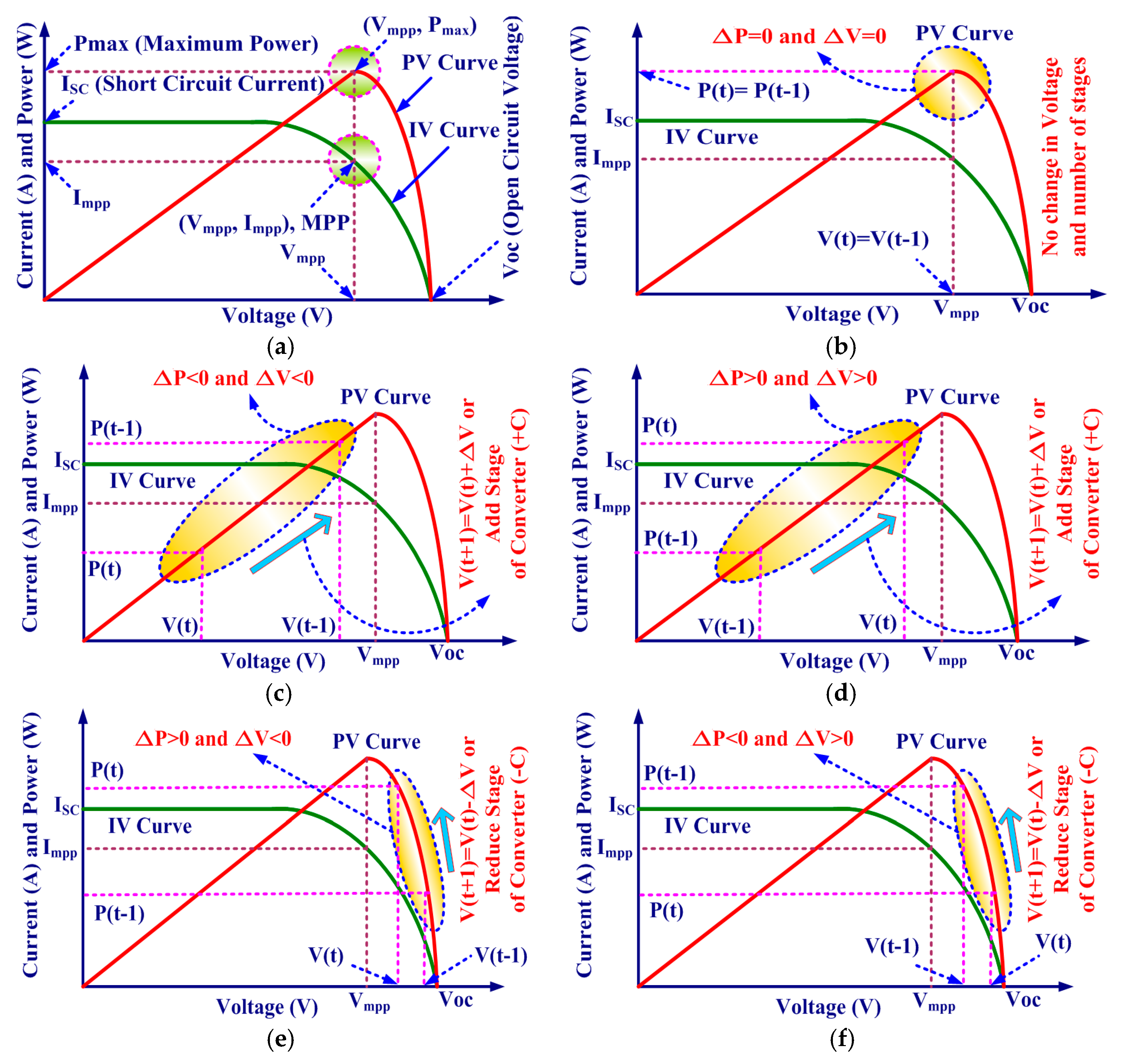
The proposed photovoltaic system (PV System) consists of PV modules, the proposed DC-DC converter, battery and the multilevel inverter (MLI) which converts the battery/proposed DC-DC converter voltage to AC voltage to power AC loads/feed in the electric grid. Some amount of power is lost during the conversion of photovoltaic energy to electric energy. The PV device maximum output power (product of voltage and current) is described by the Maximum Power Point (MPP) and it is also depends on the environmental conditions (generally on temperature and light conditions). A Maximum Power Point Tracker is compulsory to ensure the maximum power output (Pmax) of a solar PV device. The Maximum Power Point Tracker can be used to adjust its input voltage to utilize the maximum photovoltaic output power and then transform this power to supply the varying voltage requirements. When the PV voltage is increased the current will ultimately decrease, and when the PV current is increased the voltage will ultimately decrease. Depending on parameters like irradiance and temperature the MPP of the I-V curve of a PV module changes dynamically. Therefore, the MPP needs to be located by a tracking algorithm as it is not known beforehand.
To achieve the maximum power transfer from the PV module to the load it is necessary to match the load resistance R
L to the best possible output resistance of the PV module R
PV (R
mpp = V
mpp/I
mpp). Characteristic power-voltage and current-voltage graphs or curves are shown in
Figure 6a.
The output power of PV module will be zero when the photovoltaic current (I
PV) is equal to the short circuit current (I
SC) or the photovoltaic voltage (V
PV) is equal to the open circuit voltage (V
OC). Thus, it is possible to track the maximum power point (MPP) of a photovoltaic cell by regulating the operating voltage of V
PV. In [
45] Maximum Power Point Tracking is discussed for a reconfigurable switched-capacitor converter and in [
46] a perturbation and observation (P&O) algorithm is discussed for DC-DC converters connected to photovoltaic generators. The concept to control power of a multistage magnetic component-free DC-DC converter is explained in
Figure 6b–f. Thus, to regulate the operating voltage V
PV, the ON time of the capacitor and number of stages (if the structure is reconfigurable) are two controlled parameters in the proposed system, therefore it forces the MPPT charge controller to extract the maximum power PV module to operate at a voltage close to the maximum power point which causes it to draw the maximum available power from the PV module.
The proposed converter is also suitable for the DC link application in DC-AC systems where capacitor voltage balancing is the main challenge. The proposed converter also provides a viable solution for low power applications, since inductors and transformers are not required to design the proposed converter.
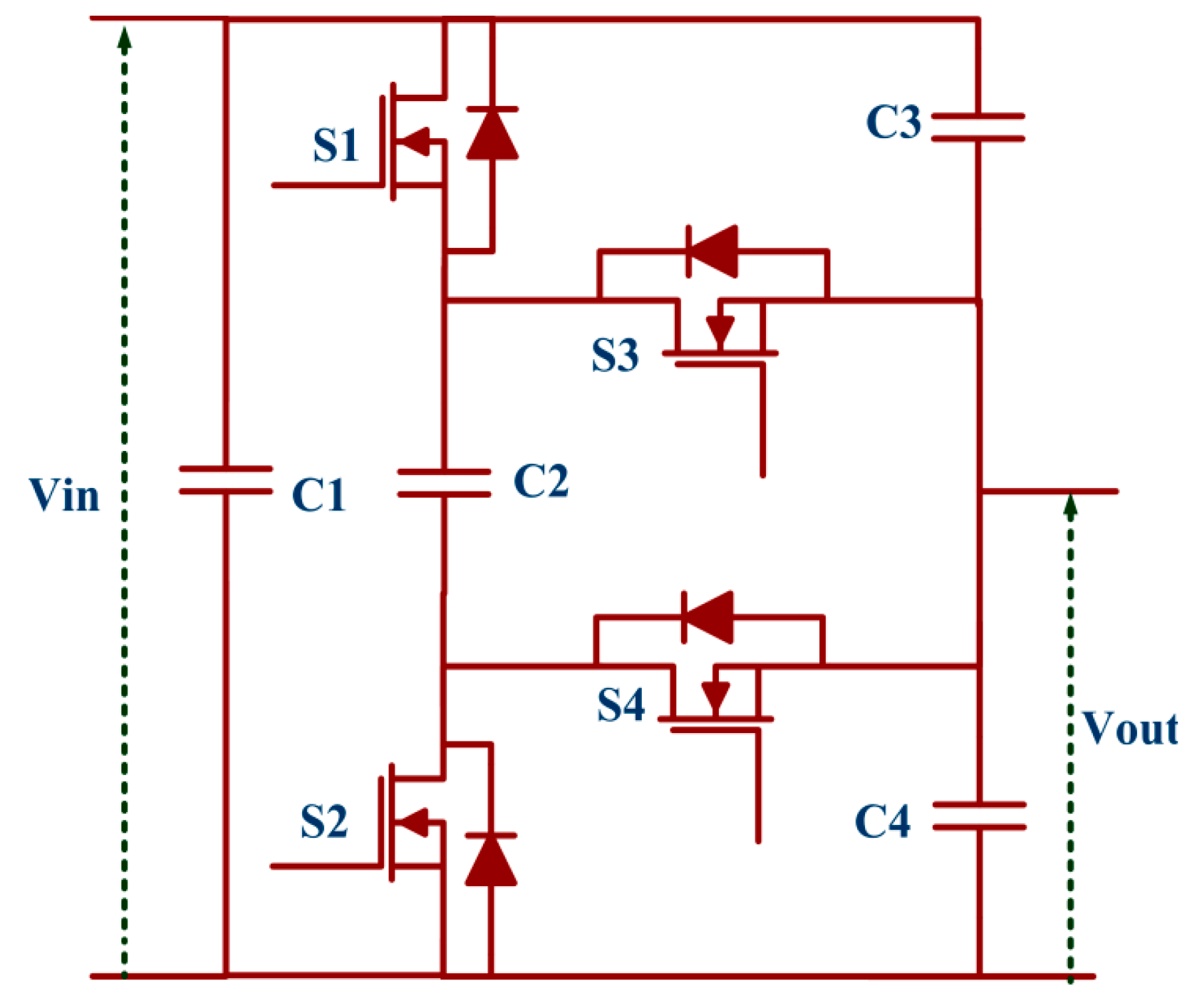
4. Design Calculation of the Capacitors of the Proposed Converter
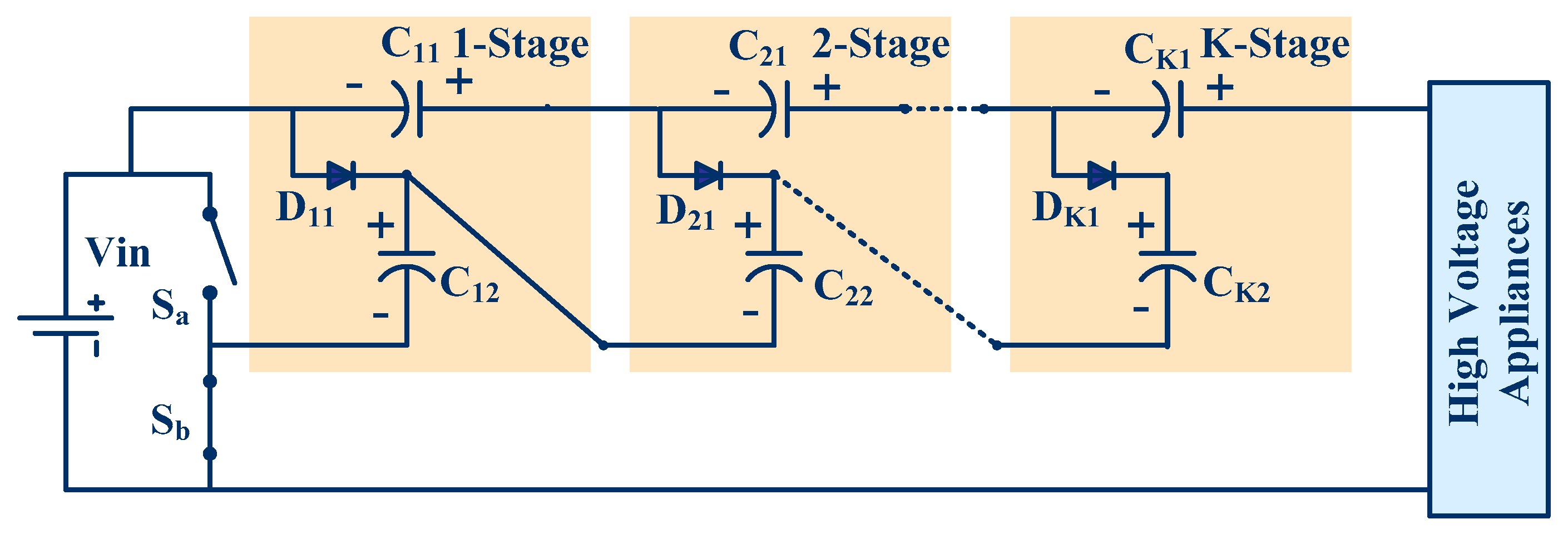
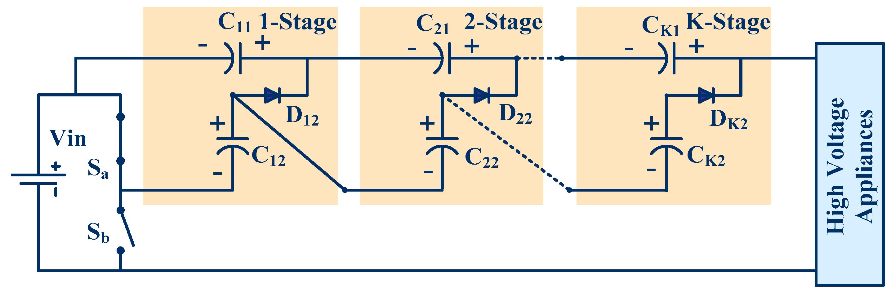
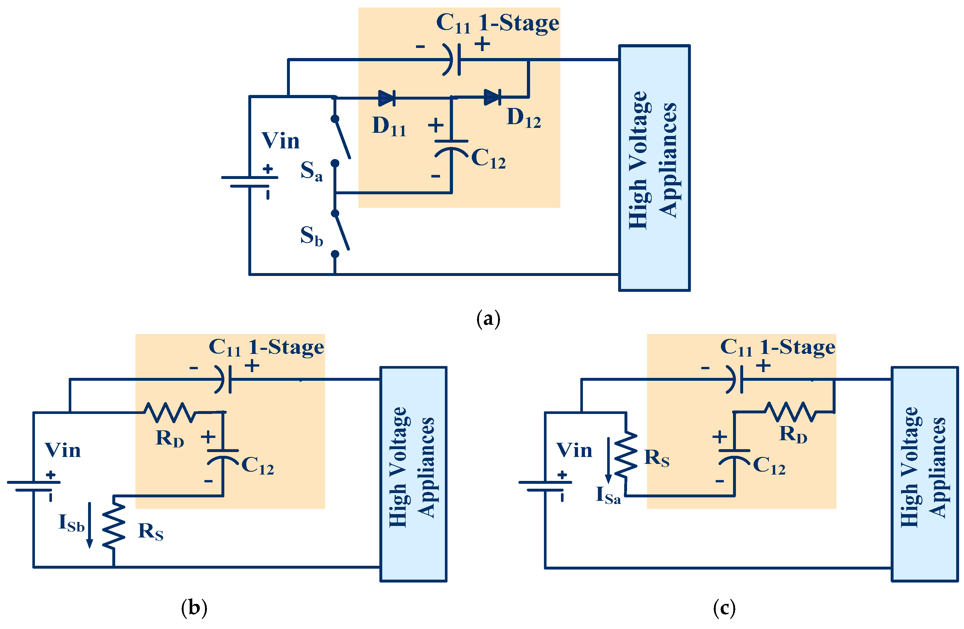
To explain the designed calculation of the proposed converter a 1-stage proposed converter is considered. The power circuit of the 1-stage proposed converter is shown in
Figure 19a. The ON state and OFF state equivalent circuit of the 1-stage proposed converter is depicted in
Figure 19b,c respectively, where R
D is the forward resistance of the diode, R
S is the forward resistance of the switch, I
Sb is the current through the switch S
b and I
Sa is the current through switch S
a.
Initially the voltage across capacitor C
12 and C
11 is zero. Capacitor C
12 is charged through a resistance R
D and R
S from a supply voltage V
in when switch S
b is closed. The voltage across C
12 does not increase to V
in instantaneously, but builds up exponentially and not linearly.
Capacitor C
11 is charged through a resistance R
D and R
S from a capacitor C
12 voltage when switch S
a is closed. Thus, when switch S
a is closed capacitors C
11 and C
12 is charging and discharging, respectively.
In steady state and at high switching frequency, the voltage across capacitor C
11 and C
12 at any instant during charging is cycled as given in Equations (25) and (26) where,
and
is the initial voltage of capacitor C
11 and C
12. If the initial storage voltage of C
11 and C
12 is positive:
If the initial storage voltage of C
11 and C
12 is negative:
The time required for the capacitor C12 to attain any value of VC12 during the charging cycle is given in Equations (27) and (28).
When the initial voltage across the capacitor is positive:
When the initial voltage across the capacitor is negative:
The time required for the capacitor C11 to attain any value of VC11 during the charging cycle is given in Equations (29) and (30).
When the initial voltage across the capacitor is positive:
When the initial voltage across the capacitor is negative:
Voltage and current of all the capacitors are the same during the complete switching cycle. Thus the equal rating of all capacitors is suitable to design the proposed converter whose voltage rating is greater than the input voltage.
6. Experimental and Simulation Results of the Proposed Self-Balanced and Magnetic Component-Free Multistage DC-DC Converter
The proposed self-balanced and magnetic component-free multistage DC-DC converter simulation and experimental results are discussed in this section. The proposed multistage converter has been designed for four stages with rated power 60 W, switching frequency 100 kHz, output voltage is 100 V and the supply voltage is 24 V. Switches Sa (here S1) and Sb (here S2) are operated complementarily with a 50% duty cycle. High switching frequency is used to reduce the rating of the capacitor.
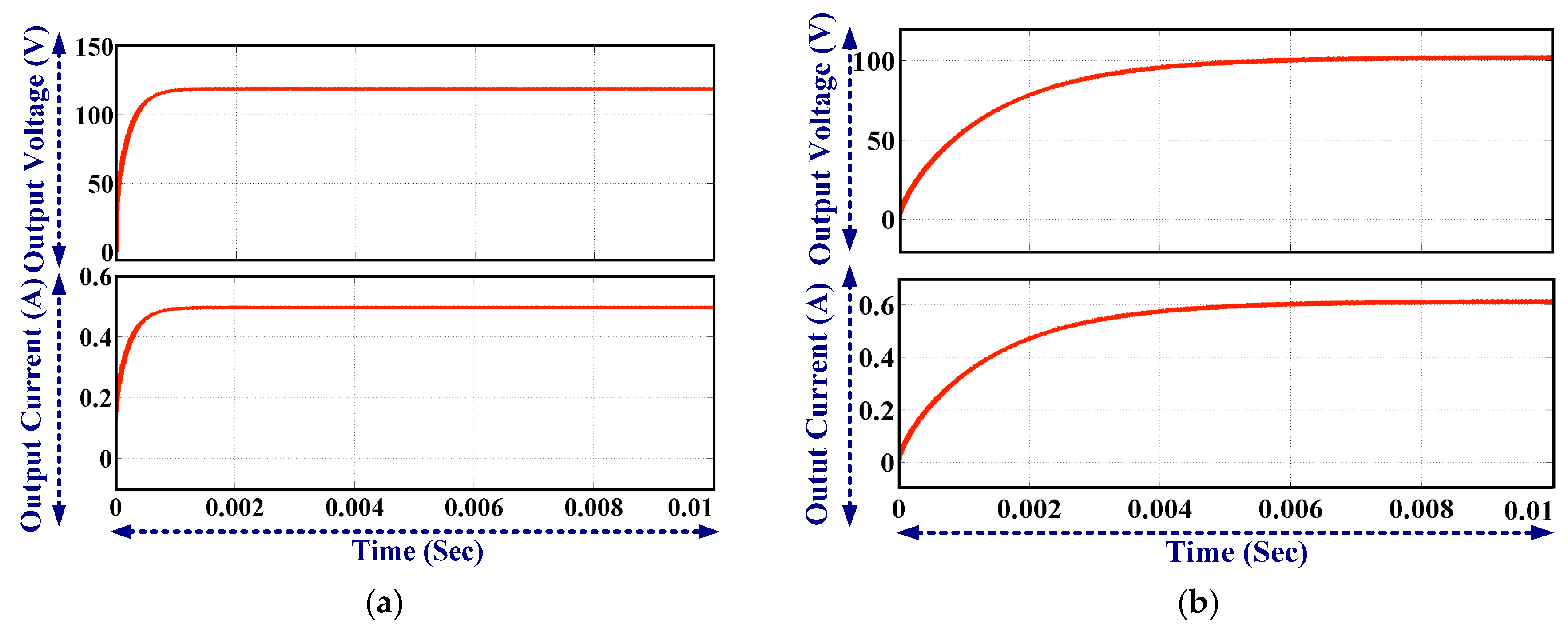
The output voltage and current waveform with ideal components (voltage drop across the switch and the diode is zero) is shown in
Figure 21a. It is observed that the settling time for the output voltage of the proposed converter with ideal components (forward resistance of the diode is 0) is less than 2 ms. The effect of voltage drop across the diode is analyzed in the previous section. The output voltage and current waveform (assuming 1 V voltage drop across the switch and diode) are shown in
Figure 21b.
It is observed that the settling time for the output voltage of the proposed converter with practical components is approximately 4 ms due to the forward resistance of the diode and switch. Thus, the practical waveform differs from the ideal waveform because of the time constant (R
D + R
S) C as explained in
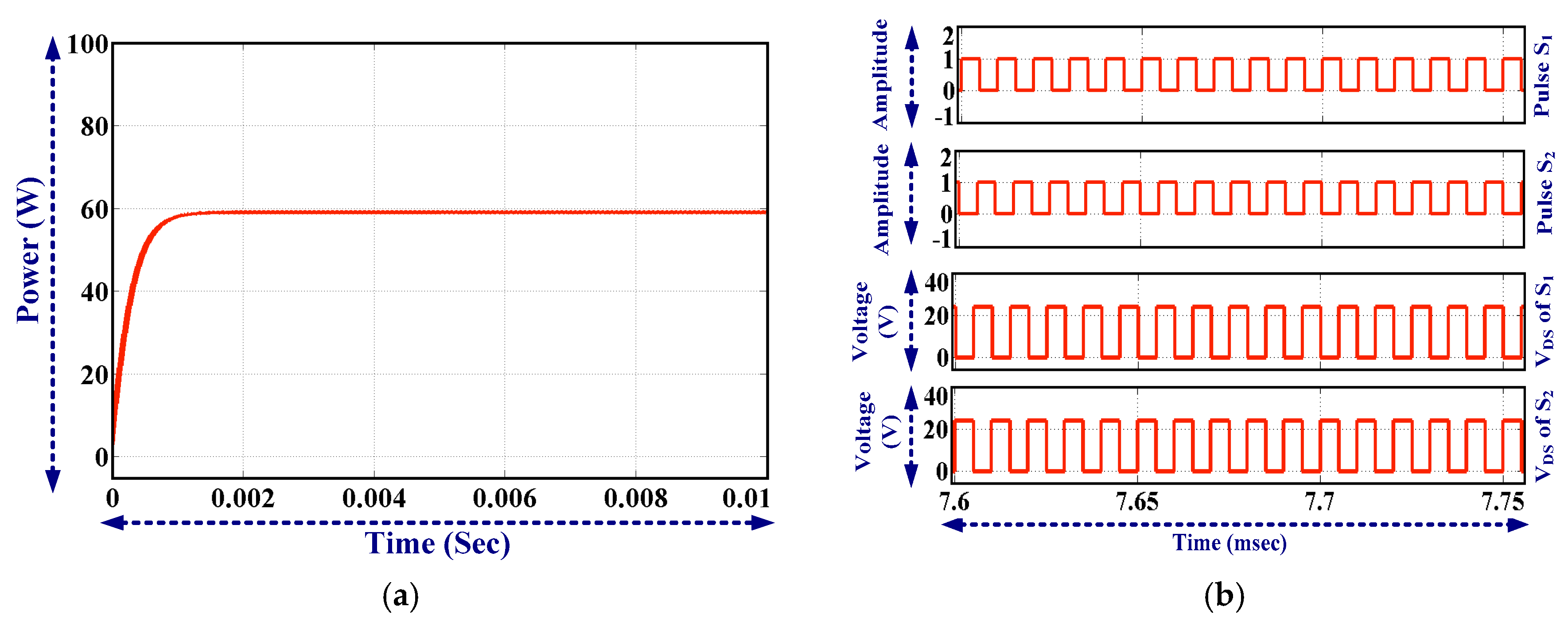
Section 4. The output power waveform and switch voltage are shown in
Figure 22a,b, respectively. The output voltage and input voltage waveform with ideal components (voltage drop across the switch and the diode is zero) are shown in
Figure 22c. The output voltage and input voltage waveform (assuming a 1 V voltage drop across the switch and diode) are shown in
Figure 22d.
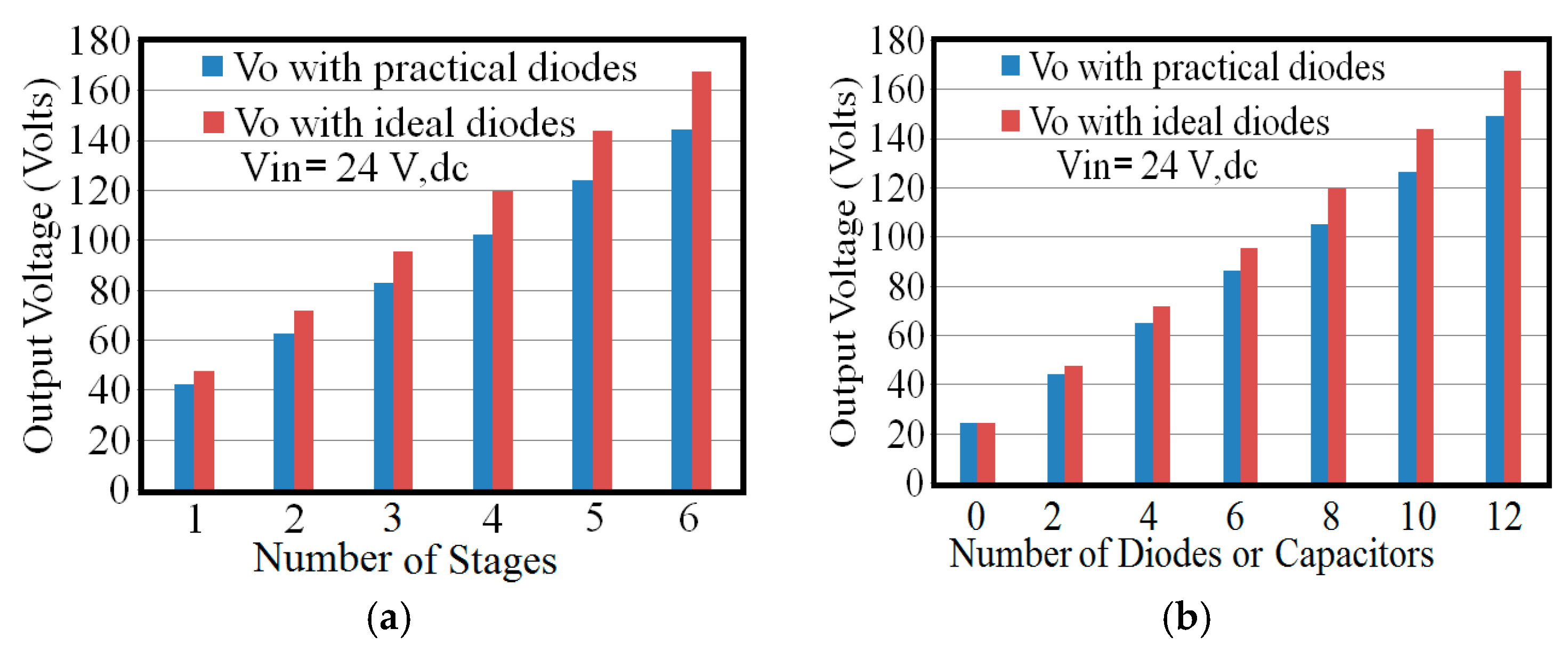
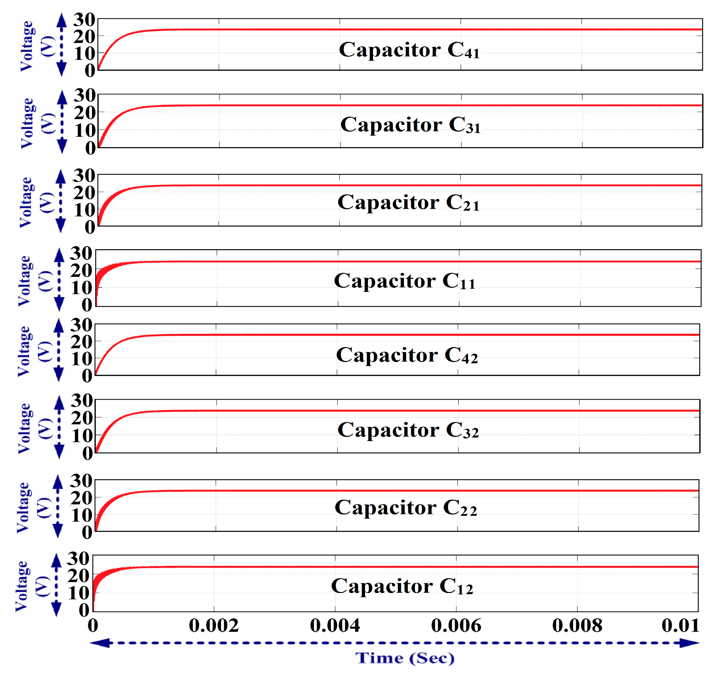
It is observed that 120 V output voltage is achieved from a 24 V input supply. Thus, ideally the voltage gain of the proposed converter is 5, which is equal to the number of stages +1. When the voltage drop across the diode is considered, an output voltage of 100 V is achieved from a 24 V supply. The voltage across the switch is equal to the input supply voltage (24 V). The voltage across all capacitors is same, which is equal to the input supply voltage (24 V) if the voltage drop across the diode is not considered. The voltage across all diodes is same (24 V) when the diode is reverse- biased. The voltage across diodes is shown in
Figure 22e–f. The voltage across the capacitors is shown in
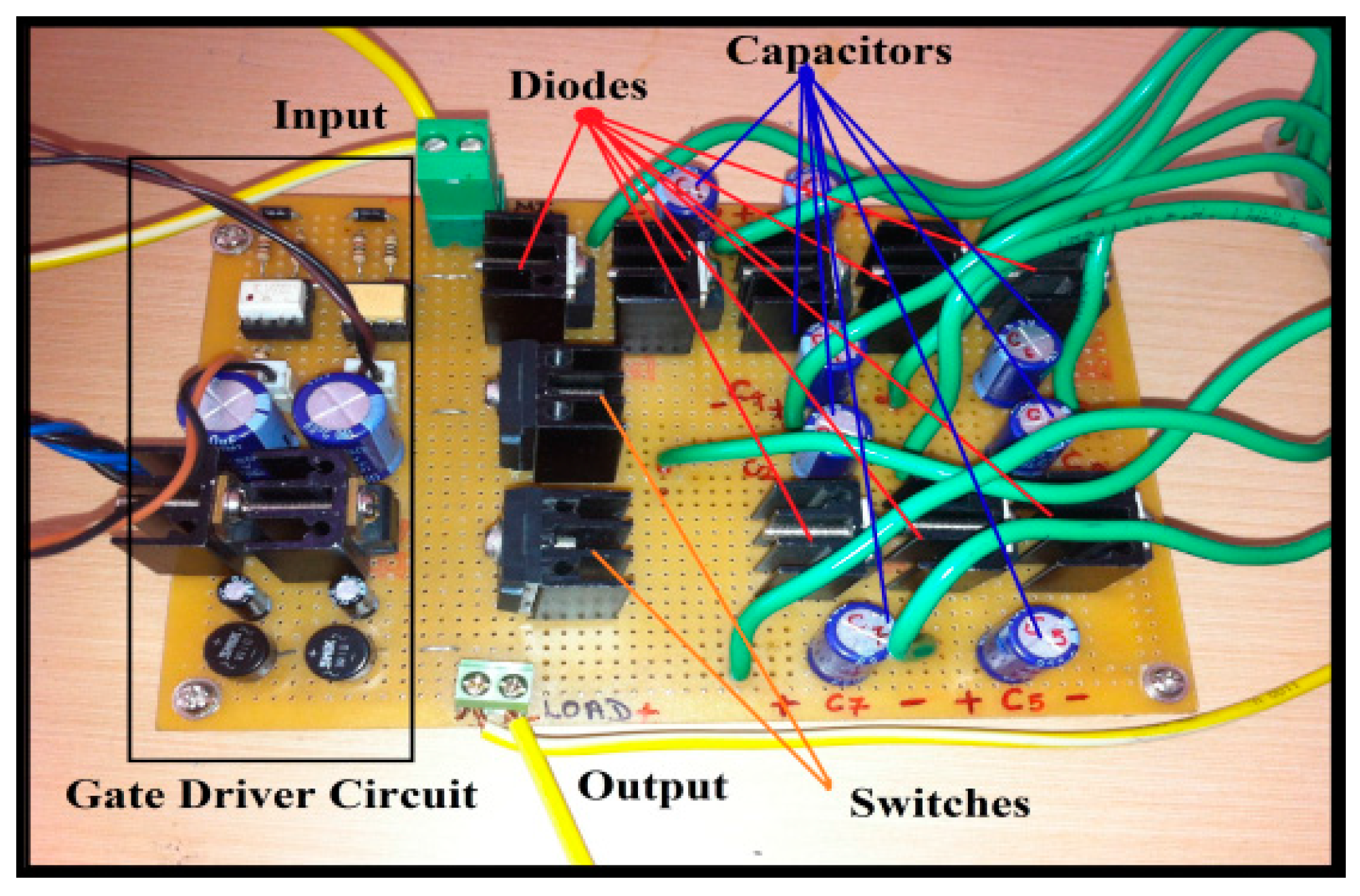
Figure 23. The proposed 4-stage self-balanced and magnetic DC-DC converter is investigated experimentally and the result shows a good match with the simulation results. The hardware components are listed in
Table 7.
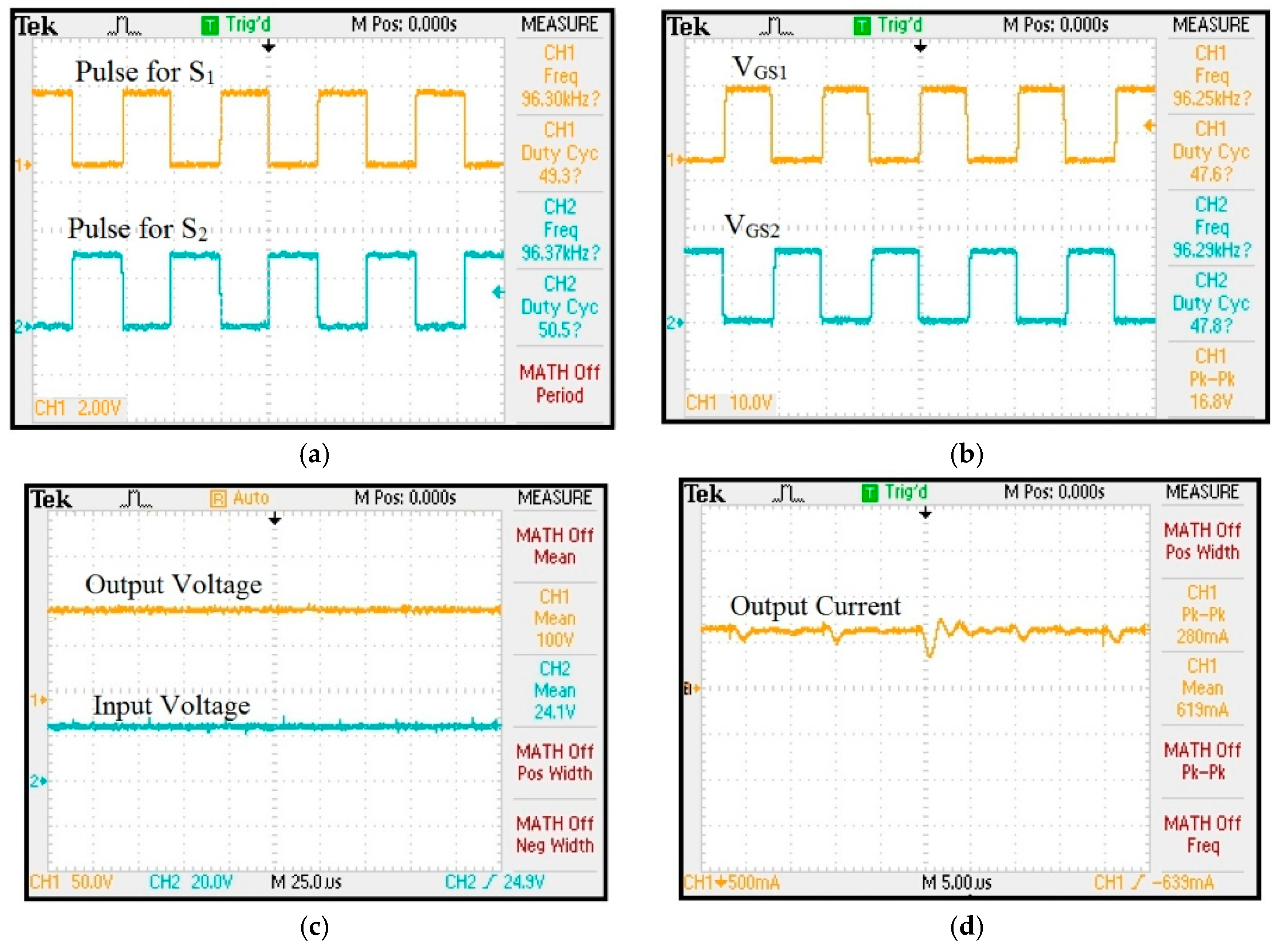
PIC18F45K20 is used to generate pulses and TLP250 is used as driver IC. The hardware prototype of the proposed converter is shown in
Figure 24.
Pulses are generated from a PIC controller and the gate driver output is shown in
Figure 25a,b, respectively. Output voltage and input voltage waveform are shown in
Figure 25c. It is observed that 100 V output is achieved from a 24 V input supply.
The output current waveform is shown in
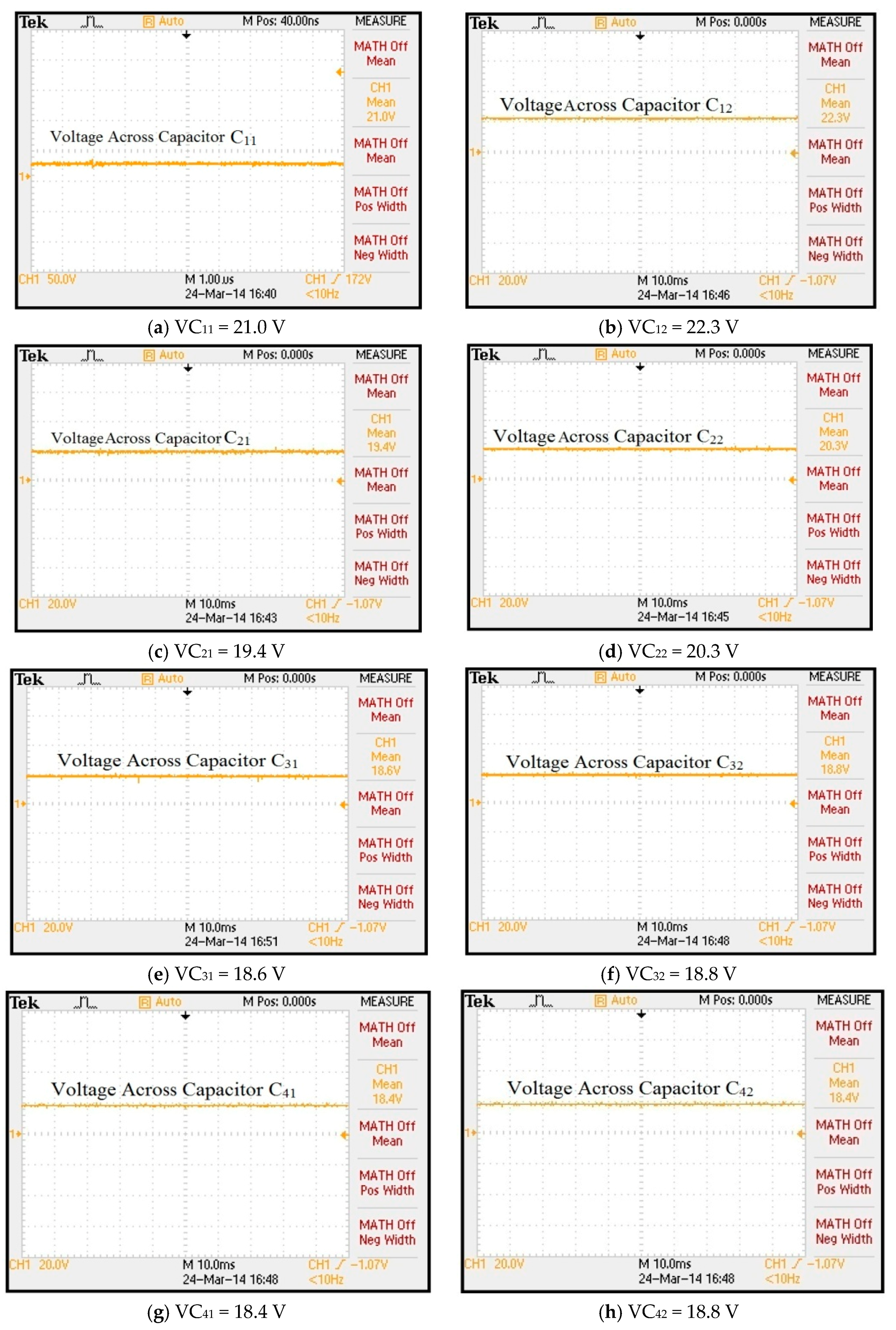
Figure 25d and it is observed that the output current is 0.619 A. The voltage across each capacitor is shown in
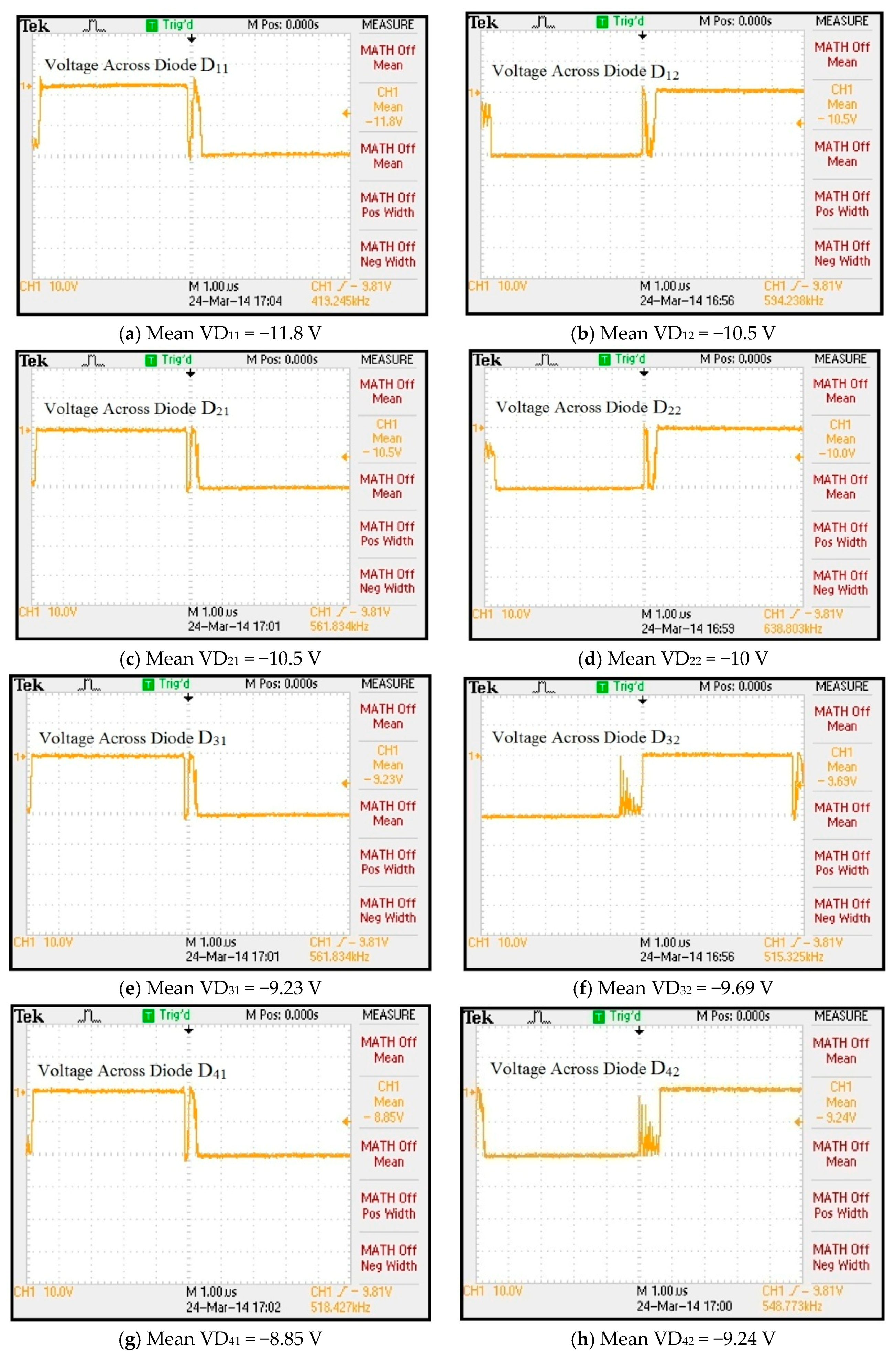
Figure 26a–h. It is observed that the voltage across each capacitor is nearly the same and slightly less than the input voltage 24 V (an effect of the diode). Voltage stress across each diode is shown in
Figure 27a–h. It is observed that the voltage stress across the diode is approximately the same and the peak voltage across the diode is slightly less than the input voltage (24 V) (an effect of the voltage drop). The voltages of all capacitors and all diodes differ slightly due to the forward resistance of the diode and switch. The lower stages (source side) capacitors are charged through the path which contain less diodes whereas as the number of stages increases the path followed for the charging of higher stage (moving towards load) capacitors contain more diodes. Thus, practically a slight difference is observed in the voltage of the capacitors.


