1. Introduction
Antireflection coating plays an important role in the improvement of short-circuit current density and photovoltaic conversion efficiency of silicon solar cells. With antireflection coating, the reflectance can be greatly decreased across the whole absorption band [
1]. To achieve minimum reflection of a normal incident wave of a single wavelength, the antireflection coating may consist of a single layer, which must possess (a) a refractive index equal to the square root of the refractive indices of the materials bounding the coating and (b) a thickness equal to one-quarter of the wavelength within the material of which the coating consists [
1], as shown in Equations (1) and (2). When the design wavelength is 550 nm (
λair), the optimal refractive index and thickness of the single-layer antireflection coating are determined as 1.85 and 74 nm (
nair = 1.00,
nSi = 3.42). Up to now, several materials have been adopted for a single-layer antireflection coating, such as TiO
2, SiO
2, and so on [
2,
3].
However, if one wants to achieve broadband antireflection coatings, additional layers must be added [
1]. For a double-layer antireflection coating, the design can be optimized with Equations (3) and (4) according to the report of Richards [
4]. The refractive indexes are stacked as follows
nSi >
n1st >
n2nd >
nair, where
n1st and
n2nd represent the refractive indexes of the first layer and second layer of the antireflection coating. When the design wavelength is 550 nm (
λair), the optimal refractive indexes and thicknesses of each layer are determined as 2.27 (
n1st), 1.51 (
n2nd), 61 nm (
d1st), and 91 nm (
d2nd). In consideration of the practical materials, Al
2O
3 was combined with TiO
2 [
5], and MgF
2 was combined with ZnS [
6] to construct the double-layer antireflection coating.
According to the report of Bouhafs et al. [
7], the design of a triple-layer antireflection coating on silicon can be optimized with Equations (5)–(7), where
n1st,
n2nd, and
n3rd are the refractive indexes of first layer, second layer, and third layer, respectively. The refractive index decreases in the order
nSi >
n1st >
n2nd >
n3rd >
nair. When the design wavelength is 550 nm (
λair), the optimal refractive indexes and thicknesses of each layer are determined as 2.52 (
n1st), 1.85 (
n2nd), 1.36 (
n3rd), 55 nm (
d1st), 74 nm (
d2nd), and 101 nm (
d3rd). Triple-layer antireflection coatings, e.g., SiO
2/SiO
2-TiO
2/TiO
2 [
1] and SiO
x/SiO
xN
y/SiN
x [
8], were adopted to decrease the reflectance and increase the efficiency of silicon solar cells.
Apparently, the triple-layer antireflection coating shows the lowest reflectance in these three structures [
1]. Therefore, the photovoltaic industry is very willing to adopt the triple-layer structure for a better photovoltaic performance. In spite of the appropriate refractive index (
n = 2.26) as the first layer of a triple-layer antireflection coating, TiO
2 seems not to be the best choice on account of its poor surface passivation capability, which is unbeneficial to the open circuit voltage of a solar cell [
1]. As for SiN
x, on the one hand, its refractive index can be easily tuned from 1.98 to 2.98 in the deposition process with the PECVD (plasma-enhanced chemical vapor deposition) method [
9]. On the other hand, resulting from the high density of fixed positive charges and high hydrogen content, SiN
x possesses outstanding surface passivation ability, which is beneficial for the improvement of an open circuit voltage [
8]. Therefore, in the photovoltaic industry, the antireflection coating is generally made up of three SiN
x layers with different refractive indexes deposited by PECVD, in consideration of the antireflection effect, surface passivation, and simplicity of the process.
Although the surface passivation effect of SiNx can be improved along with the increase of refractive index, the parasitic absorption becomes more severe. Therefore, for balance, the refractive index of the first SiNx layer is usually around 2.37 (n1st). Correspondingly, the optimal refractive indexes of the other two SiNx layers are determined as 1.85 (n2nd) and 1.44 (n3rd) according to Equation (5). When the design wavelength is 550 nm (λair), the optimal thicknesses of each SiNx layer are determined as 58 nm (d1st), 74 nm (d2nd), and 95 nm (d3rd), according to Equation (7).
However, it can be found that the refractive indexes of the second and third layers cannot be achieved by SiN
x [
9]. Therefore, Kuo et al. adopted SiO
xN
y (
n = 1.8) as the second layer and SiO
x (
n = 1.46) as the third layer [
8], both of which can be easily integrated into the SiN
x deposition process with the PECVD method. In actual production of crystalline silicon solar cells, 240 pieces are deposited with antireflection coating in a PECVD tube furnace simultaneously, which means that the control of consistency between each piece is of particular importance. When SiO
xN
y is being deposited, three gases (SiH
4, NH
3, and N
2O) need to be injected into the tube furnace at the same time, which is a big challenge for the control of consistency. Kuo et al. used the calculated optimal thicknesses (59.78, 76.39, and 94.18 nm) as the actual thicknesses of each layer, which resulted in an impressive antireflection effect [
8]. However, the entire thickness was up to 230 nm, which significantly increases the cost of the antireflection coating. In addition, on account of the fire-through silver contact metallization applied, a coating thickness up to 230 nm definitely influences the contact between silver and silicon. Therefore, to balance the cost, electrode contact, and antireflection effect, the entire thickness of the antireflection coating is usually around 80 nm in mass production.
Hence, in this report, in order to seek a more feasible antireflection coating structure with lower reflectance in mass production, SiOx was adopted to replace the third layer of traditional, triple-layer SiNx antireflection coating, preserving the other two layers. This new kind of antireflection coating was applied to improve the efficiency of a monocrystalline silicon PERC (passivated emitter and rear cell) solar cell, which is anticipated to dominate the photovoltaic market in the next few years.
2. Materials and Methods
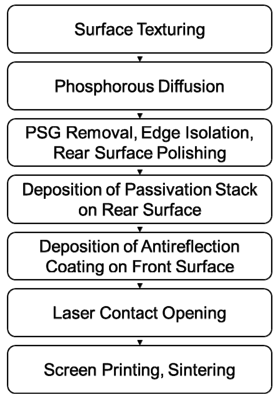
Boron-doped monocrystalline silicon wafers with a length of 156.75 mm, thickness of 180 μm, and resistivity of about 0.8 Ω·cm were adopted. The manufacturing process flow of an industrialized monocrystalline silicon PERC solar cell is shown in
Figure 1.
The as-cut monocrystalline silicon wafers were firstly textured with an alkali-based etching solution. Then, the samples were transferred into a tubular furnace to complete phosphorous diffusion and emitter formation. Subsequently, phosphosilicate glass (PSG) removal, edge isolation, and rear surface polishing were accomplished with a wet etching technique. After that, the aluminum oxide and silicon nitride were deposited by ALD (atomic layer deposition) and PECVD successively to form the passivation stack (Al2O3/SiNx) on the rear surface. Afterwards, the PECVD was still used to deposit the antireflection coating on the front surface. After the Al2O3/SiNx stack was locally opened by laser ablation, the electrode pastes (rear-side silver, rear-side aluminum, and front-side silver) were screen-printed and dried. Finally, the samples were sintered in a mesh belt furnace to complete the metallization and finish the solar cell manufacturing process.
During the deposition of the antireflection coating, the gas sources were changed to adjust the layer composition. For SiNx, silicane (SiH4) and ammonia (NH3) were adopted as the gas sources. And for SiOx, the ammonia was replaced by laughing gas (N2O). In detail, two SiNx layers with different refractive indexes (n = 2.37 and n = 2.09) and one SiOx layer (n = 1.46) were combined to form the triple-layer antireflection coating. As mentioned above, the control of consistency is particularly important because 240 samples are simultaneously fabricated in a tube furnace. The gas flows (SiH4 and N2O), pressure, radio-frequency power, and temperatures of different zones were adjusted and optimized in order to improve the consistency. The results shown below were obtained after the optimization. For comparison, the traditional SiNx triple-layer antireflection coating was also adopted to manufacture solar cells, i.e., employing the SiNx layer with a refractive index of 1.99 as the third layer.
After the completion of the whole manufacturing process flow of the solar cell, the passivation of carrier-induced defects was conducted by current injection to suppress the severe light-induced degradation of the PERC solar cell.
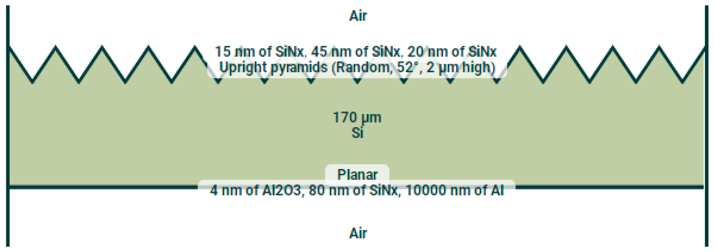
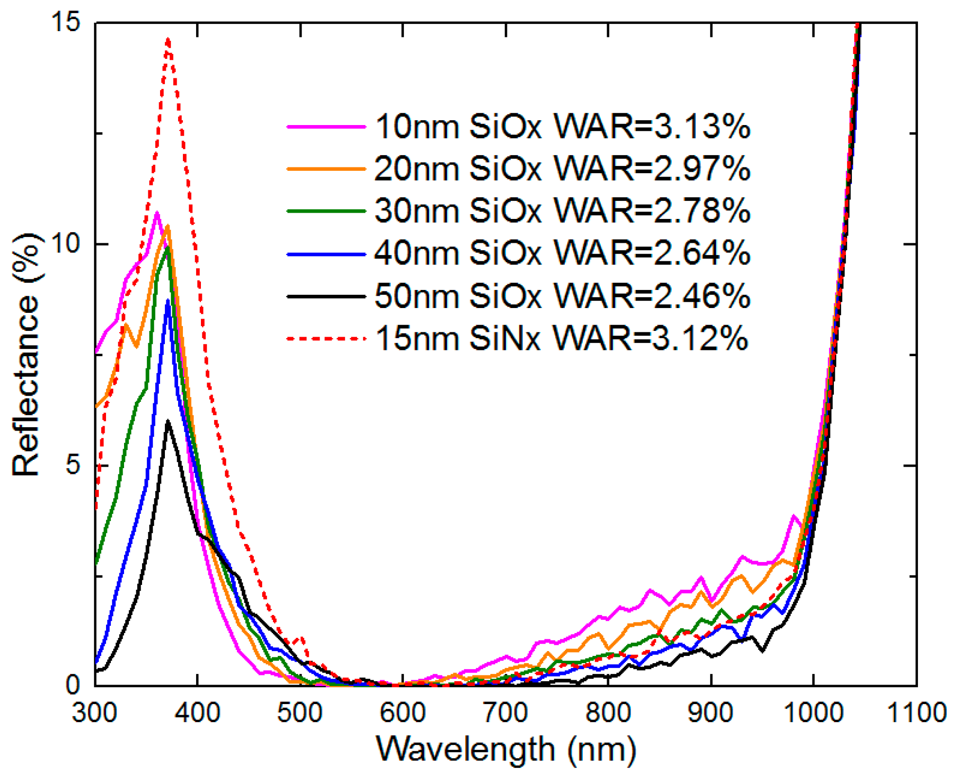
Before the experiment, a theoretical analysis was conducted to explore the optimal thickness of the SiO
x layer. As for textured wafers, the light travels through the antireflection coating obliquely, which will increase the optical path length. Additionally, the fraction of light initially reflected from the surface can hit the surface a second time and has another opportunity to enter the wafer [
10]. Therefore, in view of these differences with planar wafers, a simulation software called SunSolve from PV Lighthouse was adopted, instead of the equations mentioned above, to further improve the accuracy of the theoretical analysis. Combining Monte Carlo ray-tracing with thin-film optics, SunSolve can determine the optical losses in a solar cell or solar module under a chosen spectrum [
11].
As shown in
Figure 2, the simulation structure consisted of a triple-layer antireflection coating, a random upright pyramid texture with a height of 2 μm, a monocrystalline silicon wafer with a thickness of 170 μm, a planar rear surface, an Al
2O
3/SiN
x passivation stack, and an aluminum electrode from top to bottom. The front busbars and fingers were excluded to focus on the antireflection coating.
The simulation parameters of the triple-layer antireflection coating are listed in
Table 1. The parameters of the first SiN
x layer and second SiN
x layer were fixed as 20 nm (
n = 2.37) and 45 nm (
n = 2.09), respectively. The parameters of the third layer were adjusted, including material, refractive index, and thickness.
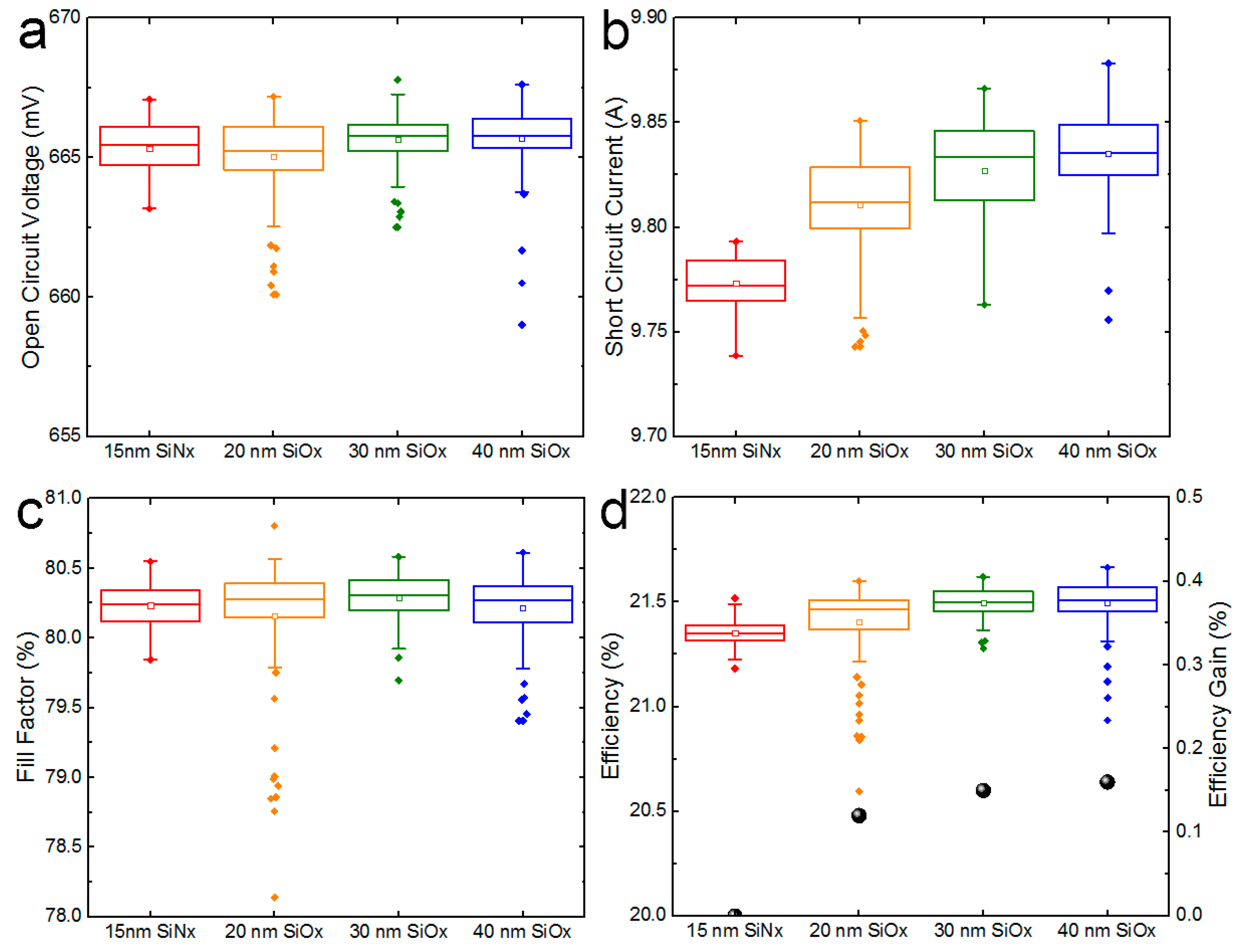
4. Further Discussion
In the results above, there is a lack of internal quantum efficiency data, which are essential in assessing the parasitic absorption of antireflection coating. Therefore, in order to solve this problem, new solar cell samples with different third layers (i.e. 15 nm SiN
x and 30 nm SiO
x) of antireflection coating have been fabricated recently. Each group contained about 400 solar cells, and the mean photovoltaic parameters are listed in
Figure 7. It should be noted that because several other optimization methods have been applied, such as wafer resistivity reduction, phosphorus-doping profile adjustment, and surface passivation improvement with a thermally grown SiO
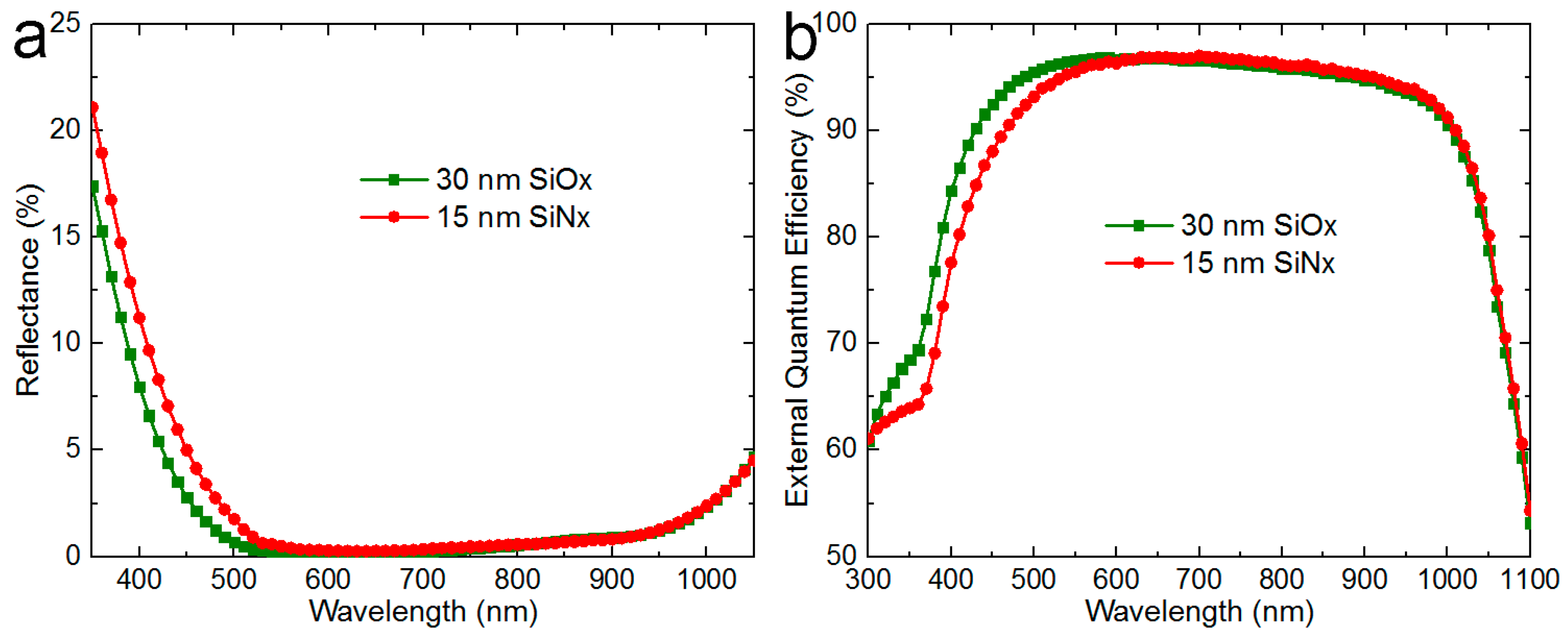
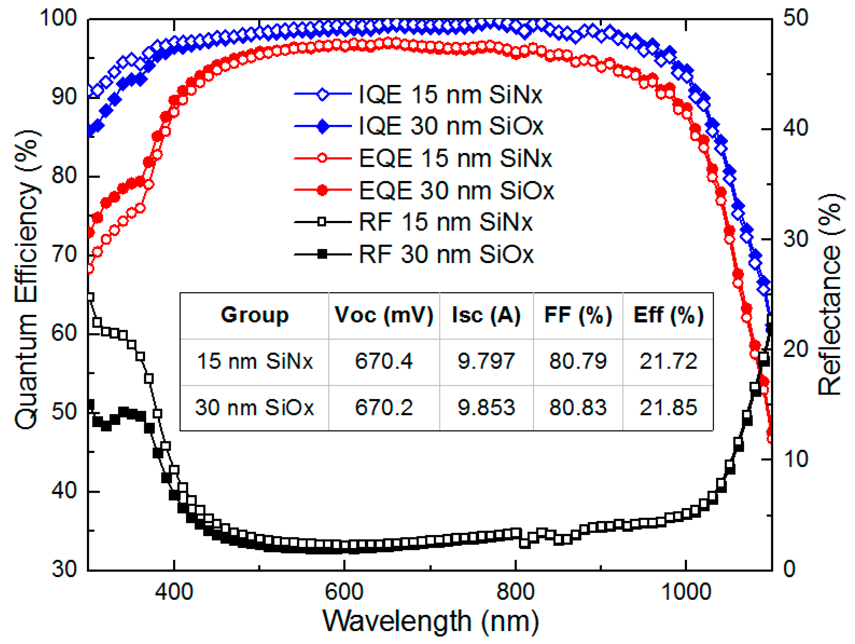
2 thin layer (~2 nm), photovoltaic performance has made good progress. On this basis, the alteration of the third layer of antireflection coating leads to a short-circuit current gain of 56 mA and an efficiency gain of 0.13% (abs.), when the open circuit voltage and fill factor remain almost unchanged. The reflectance, external quantum efficiency, and internal quantum efficiency of two kinds of solar cells were measured, as shown in
Figure 7. It can be found that the reflectance and EQE improved in short wavelengths after the alteration, which was consistent with the previous results. On the contrary, the IQE suffered a decline below about 400 nm. On the one hand, the altered layer of antireflection coating was the third layer, which was not in direct contact with the silicon substrate. On the other hand, the open circuit voltage barely changed according to both previous and current results. Therefore, it is believed that the surface passivation will not be influenced by the alteration of the third layer of antireflection coating. Correspondingly, the IQE decline below about 400 nm could be ascribed to the increase in parasitic absorption, which may be induced by SiO
x.
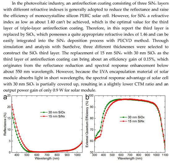
As a matter of fact, except the optimization for air in this report, the antireflection coating of the solar cell can be optimized directly for the glass/EVA encapsulation, which is expected to be more beneficial for the improvement of the solar module’s output power. However, this strategy is somewhat infeasible, because almost all of the characterization methods for solar cells are conducted in air, such as IV (current-voltage), QE (quantum efficiency), and reflectance. Nevertheless, the differences between these two strategies can be discussed according to theoretical calculations and experimental results. As mentioned above, the refractive index of the first SiNx layer of antireflection coating is usually around 2.37. According to Equation (5) (nair is replaced by nEVA), the optimal refractive indexes of the other two SiNx layers are determined as 2.26 (n2nd) and 2.15 (n3rd) for the glass/EVA encapsulation (nglass = nEVA = 1.50). In contrast, the values are 1.85 (n2nd) and 1.44 (n3rd) for air, which are much lower than those for encapsulation. From another viewpoint, the gain/loss induced by the different optical environments can be estimated according to the experimental results. When the SiNx third layer of antireflection coating is replaced by SiOx, the relative performance improvements of the solar cell and the solar module are 0.70% (absolute 0.15%) and 0.30% (absolute 0.9 W), respectively. It can be deduced that the performance gain in solar cells is reduced by 57% when implementing the SiOx in the modules.
5. Prospects
In this report, a triple-layer structure was adopted to construct the antireflection coating of monocrystalline silicon PERC solar cells. However, only the third layer of antireflection coating was adjusted and optimized, the other two layers were fixed. This structure modification brought about an efficiency gain of 0.15% for the solar cell. It can be expected that if the other two layers also take part in the optimization of antireflection coating, the reflectance and conversion efficiency of the solar cell will be further improved.
On the other hand, except for further improvement in the solar cell, attention should also be paid to the solar module. The absorption of EVA encapsulation material in short wavelengths results in the partial cover-up of the spectral response advantage of the solar cell with SiOx as the third layer, which leads to an output power gain of only 0.9 W for solar module. Therefore, through enhancing the encapsulation material transmittance in short wavelengths, the CTM ratio can be increased, and a higher output power gain is expected to be achieved.
At present, further optimization of antireflection coating is in progress, and an average efficiency gain of 0.2% for solar cells has been achieved. Combined with wafer resistivity reduction, phosphorus-doping profile adjustment, and surface passivation improvement, the average efficiency of monocrystalline silicon PERC solar cells grows to 21.93%. It should be noted that if selective emitter technology is applied, the solar cell efficiency is expected to reach 22.1%. For solar modules, cooperation needs to be established with suppliers to decrease the absorption of encapsulation material in short wavelengths without deteriorating the reliability of the solar module.
6. Conclusions
In the photovoltaic industry, an antireflection coating consisting of three SiNx layers with different refractive indexes is generally adopted to reduce the reflectance and raise the efficiency of monocrystalline silicon PERC solar cells. However, because of the physical constraint of SiNx, a refractive index as low as about 1.40 cannot be achieved, which is the optimal value for the third layer of triple-layer antireflection coating. Therefore, in this report, the third layer is replaced by SiOx, which possesses a more appropriate refractive index of 1.46, and it can be easily integrated into the SiNx deposition process with the PECVD method. Through simulation and analysis with SunSolve, three different thicknesses, i.e., 20 nm, 30 nm, and 40 nm, were selected to construct the SiOx third layer. Compared with 15 nm SiNx, the SiOx third layer can increase the short-circuit current of the solar cell, resulting in a higher conversion efficiency. Although the solar cell efficiency increases along with the increasing thickness of the SiOx third layer, a 30 nm thickness is the optimal choice because it has very similar efficiency gains and consumes less raw materials compared to a 40 nm thickness. The replacement of 15 nm SiNx with 30 nm SiOx as the third layer of antireflection coating can bring about an efficiency gain of 0.15%. According to the reflectance and EQE measurements, this efficiency improvement originates from the reflectance reduction and spectral response enhancement below about 550 nm wavelength. However, the IQE declines below about 400 nm on the contrary, which could be ascribed to the parasitic absorption increase induced by SiOx. As for the solar module, because the EVA encapsulation material absorbs light in short wavelengths, the spectral response advantage of solar cells with 30 nm SiOx is partially covered up, resulting in a slightly lower CTM ratio and an output power gain of only 0.9 W for the solar module. The LID and PID test results show that this new kind of triple-layer antireflection coating will not negatively affect the reliability of the solar module, and it can be applied in mass production.

 ,
, 


