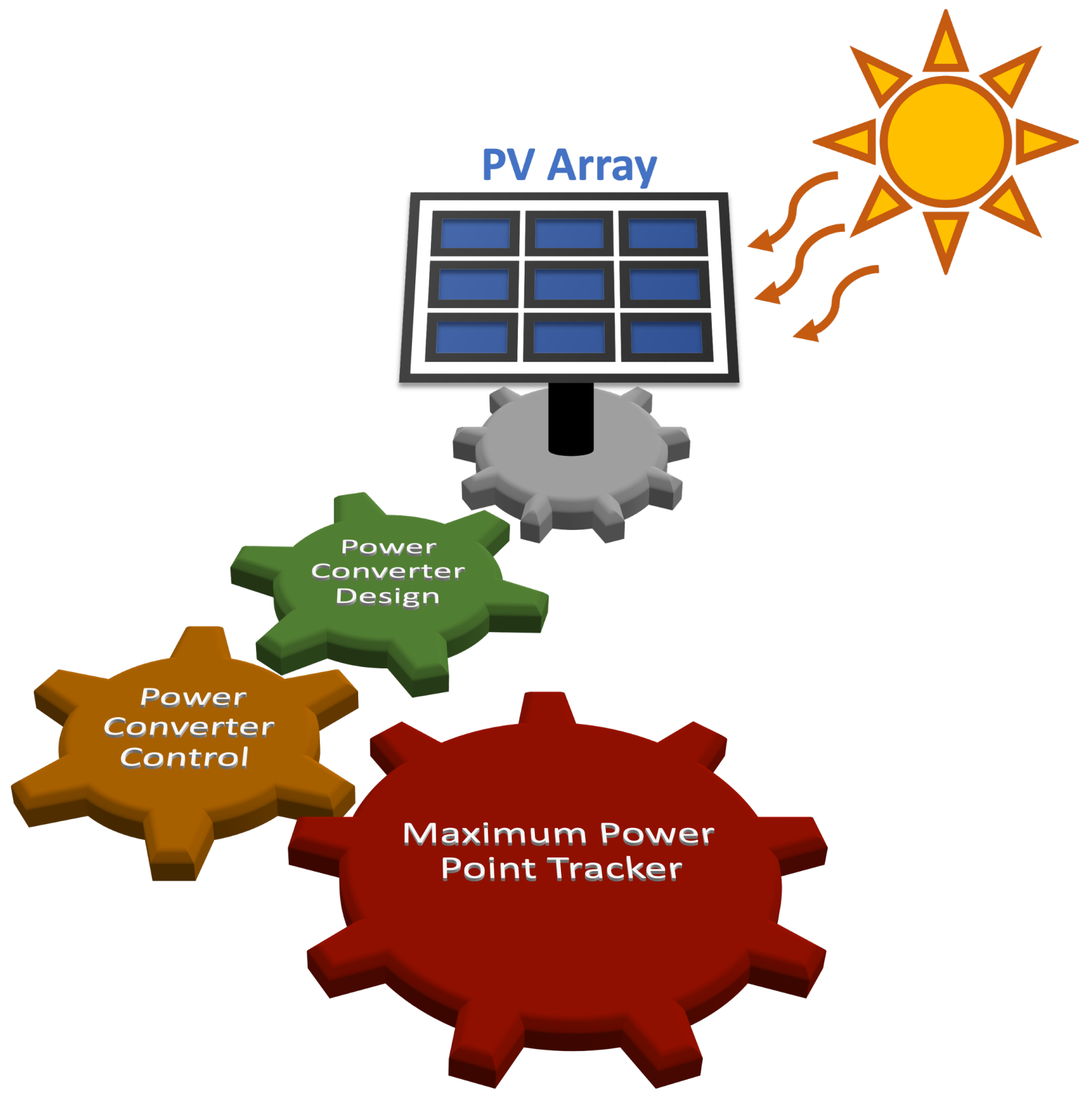
6.1. PV Array
For this particular case study, the PV array structure was designed for a nominal 5 W application with a maximum achievable power of 10 W; thereby, to fulfill the requirements, the PV array is composed of two series-connected FIT0600 semi-flexible monocrystalline solar panels, since DFRobot
® claims in [
36] that each module can efficiently deliver 5 W of output power, which is transduced to an output voltage of 5 V (
) at 1 A (
) when operating at the MPP. Consequently,
Table 2 summarizes the main parameters of each FIT0600 PV module.
Thus, the maximum expected output power from the module array is estimated to be 10 W, as the series connection of the modules lead to a maximum of 10 V at
with a maximum current of 1 A at
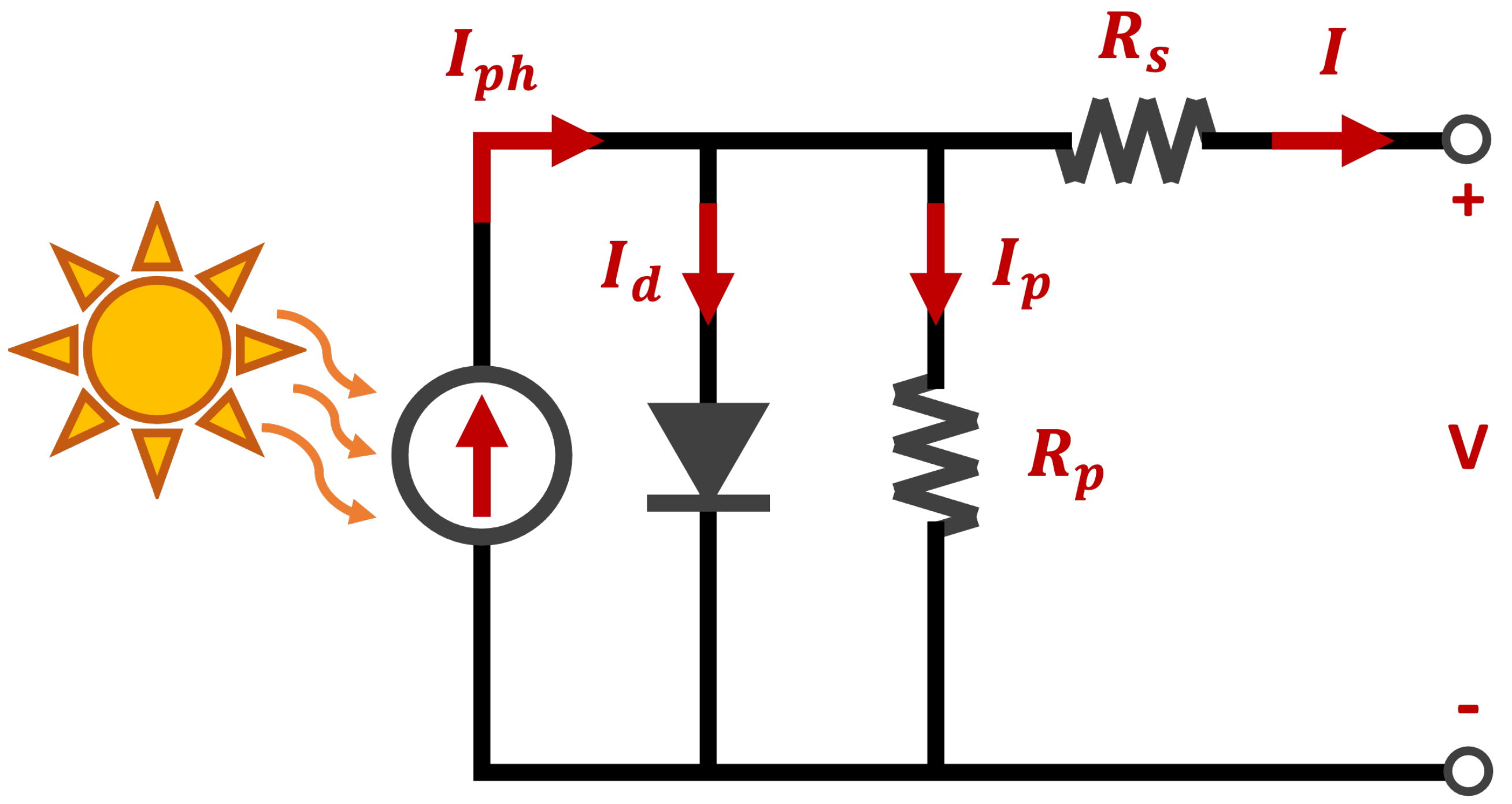
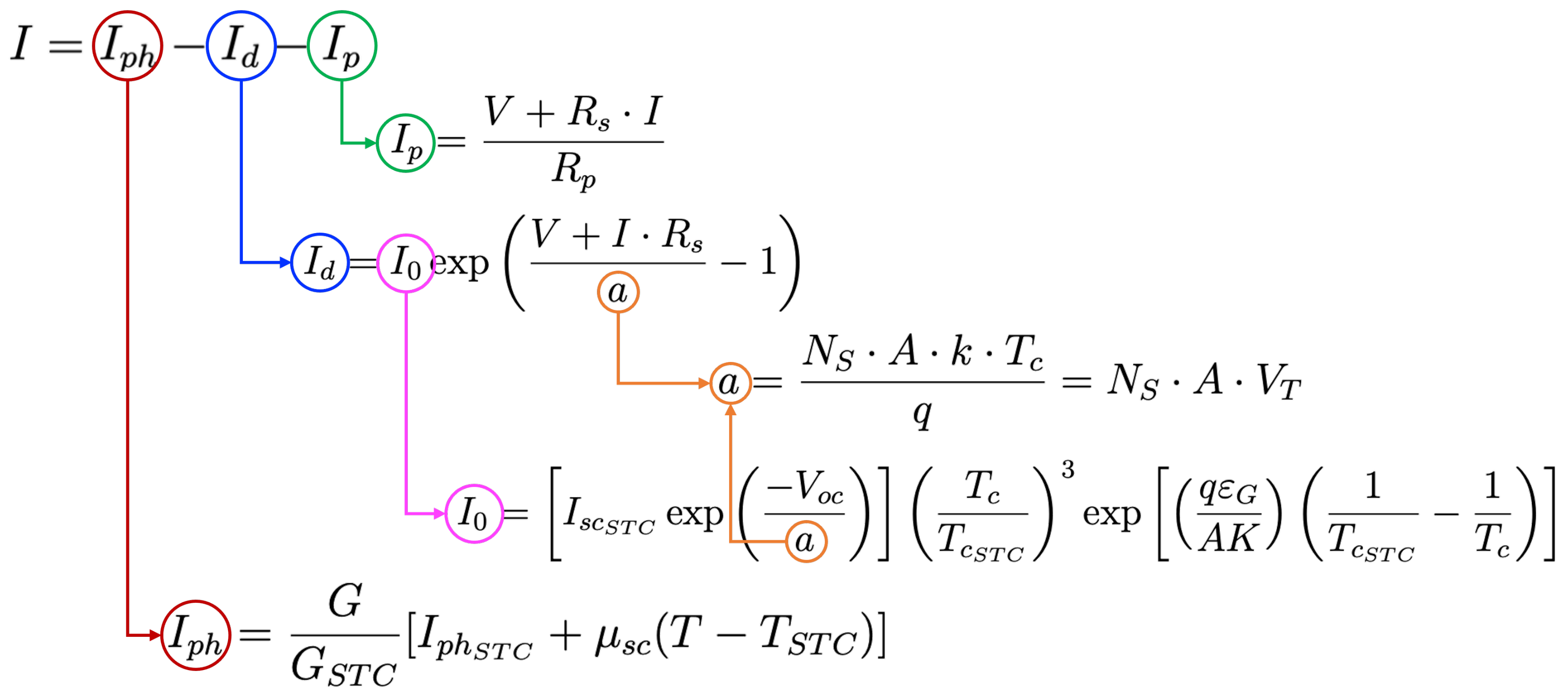
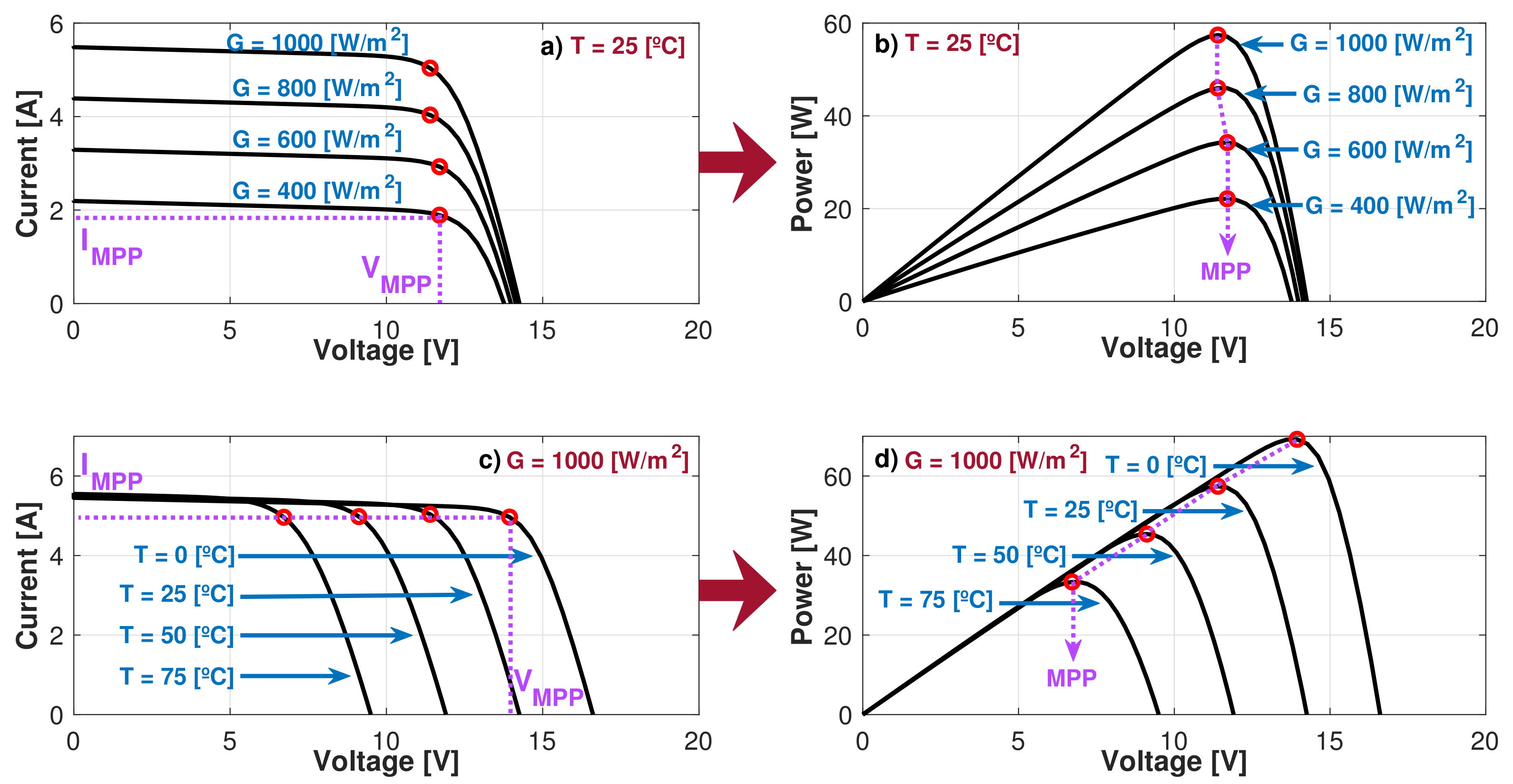
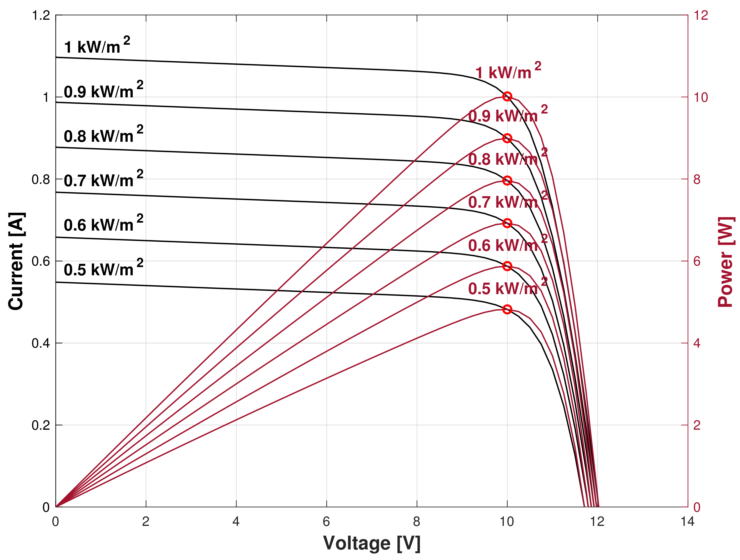
. Nevertheless, it is important to address the dynamic behavior of the PV array, which can be better analyzed through characterization of the power and current against voltage profiles, which were estimated through the mathematical model from
Section 2 and are presented in
Figure 14.
Additionally from
Figure 14, it is worth highlighting that currents vs. voltage profiles were plotted against the left-hand vertical axis; meanwhile the right-hand axis presents the power vs. voltage features of the modules. On the other hand, the maximum power points (MPPs) are highlighted with red circles on each plot to address how the MPPs move under different solar irradiation conditions. Then, the profiles from
Figure 14 also allow validation of the suitability of the designed PV array for the proposed case study, which would allow the DC–DC converter to operate at a maximum of 10 W under STC conditions.
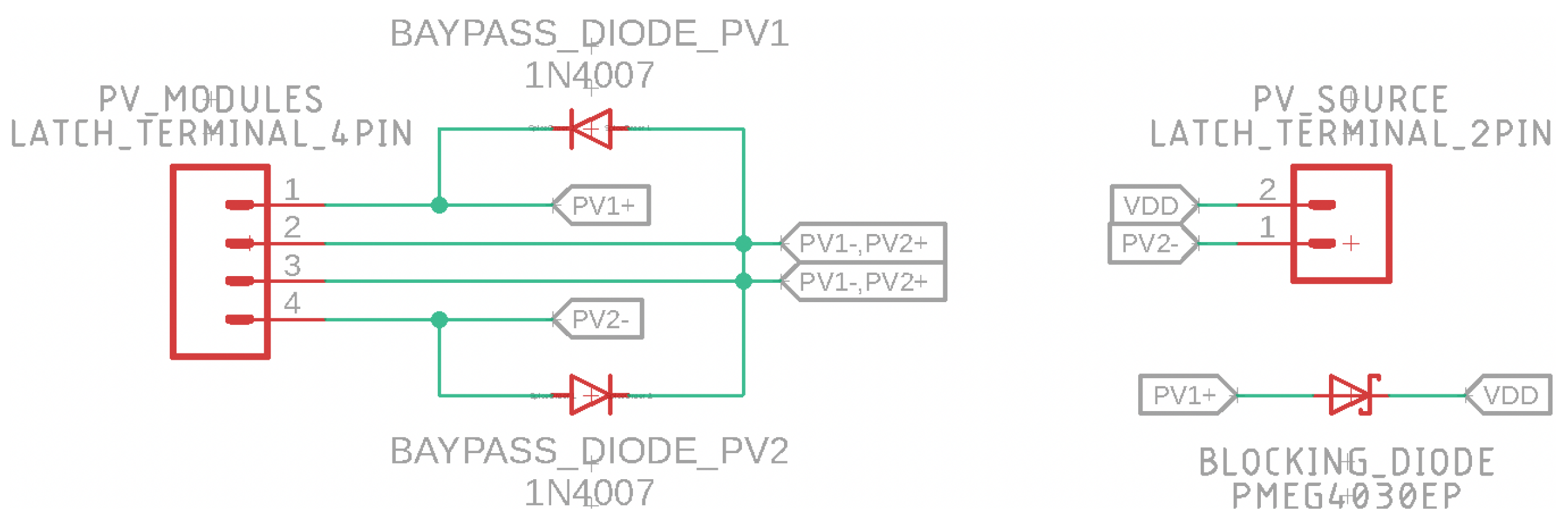
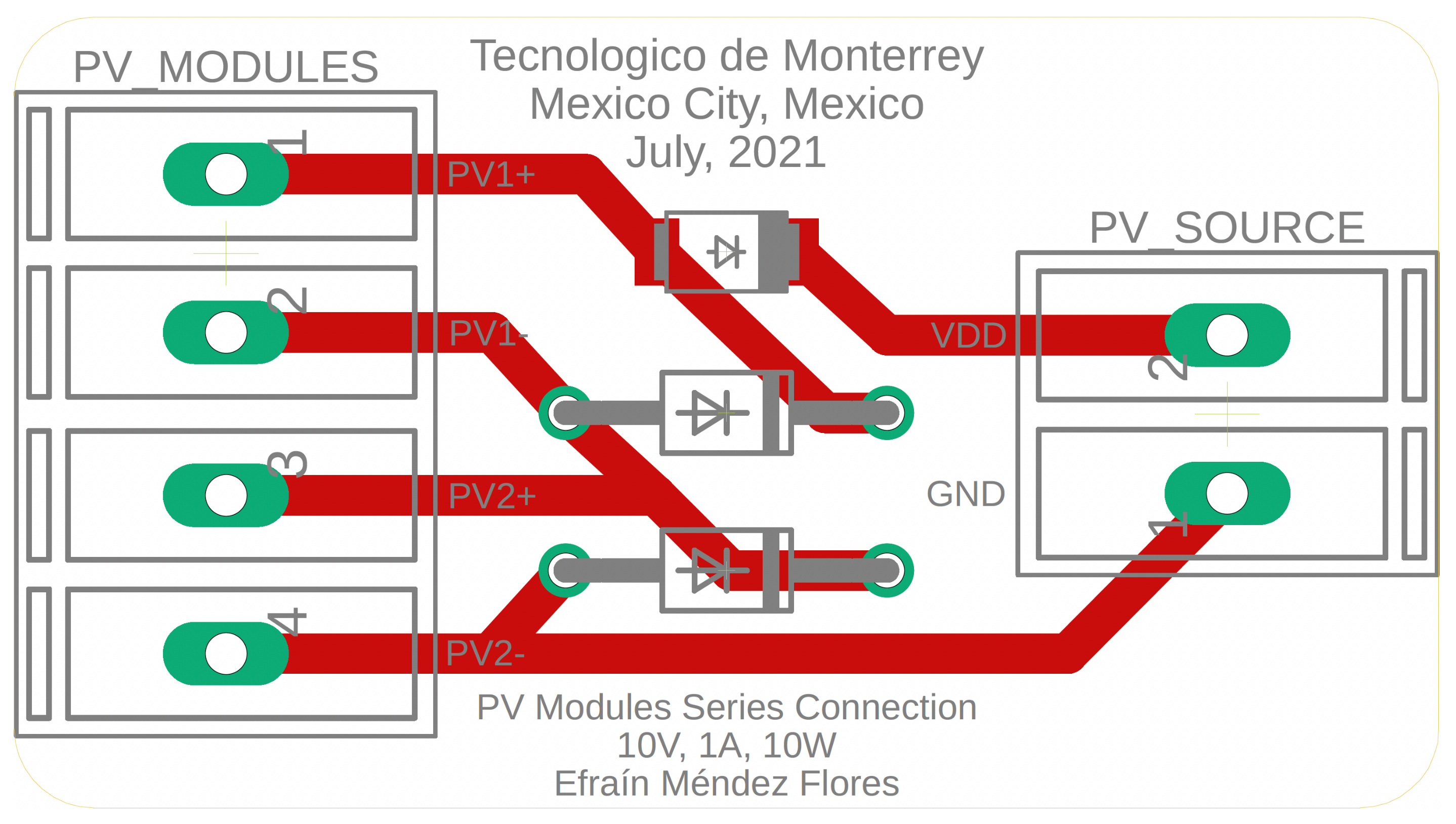
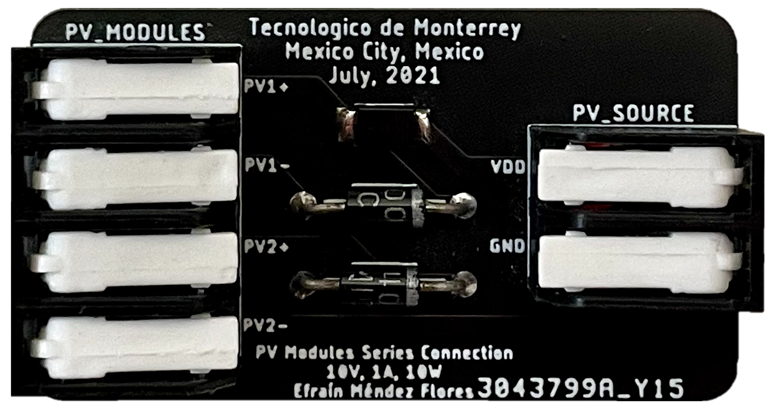
Moreover, to ensure reliable and safe connections between the photovoltaic modules and the DC–DC converter, a PCB was designed to avoid the risk of any connection errors throughout the experimental trials. Consequently,
Figure 15 shows the schematics diagram of the designed circuit, where it can be also seen how both of the PV modules are internally connected in series to provide a single PV source for the DC–DC converter.
Additionally,
Figure 15 shows where bypass diodes were added to the circuit, since those are a standard addition to prevent hot-spot phenomena, which, as explained by Solar Edge in [
37], can produce serious damage to solar cells in the array, even causing them to ignite, particularly when sunlight does not uniformly hit the surface of the PV cells in the array.
Nevertheless, it is still important to highlight that the bypass diodes ideally do not provide any efficiency liability to the system, since they are acting as additional protection to the circuit and do not act when the PV array is operating in normal irradiation conditions—in other words, under conditions where both solar panels receive the same amount of solar energy on their surface. On the other hand, it is also clear in
Figure 15 that we selected a Schottky diode as the blocking diode, since the blocking diode is continuously in contact with the output power supplied by the array and its only objective is to block reverse energy flow from the converter into the PV array. Thereby,
Figure 16 presents the PCB layout designed from the schematics from
Figure 15.
In order to address the transition from circuit conceptualization to the manufacturing stage, the PCB design from
Figure 16 was developed into an experimental PCB for the portable testbed;
Figure 17 shows the printed board circuit with all the soldered elements, for which it can be analyzed that the PCB was designed as intuitively as possible, with multiple labels to ensure proper connections.
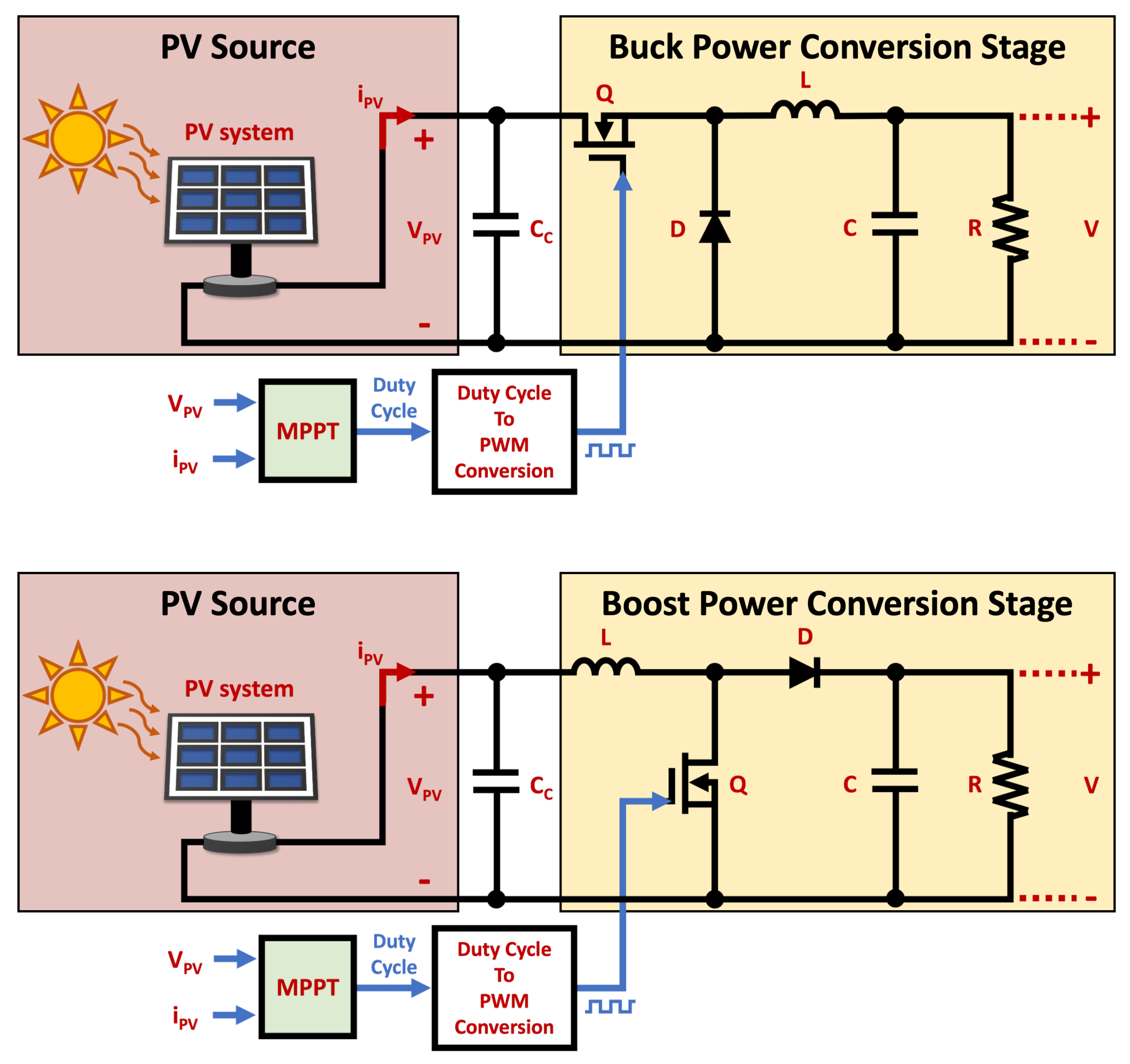
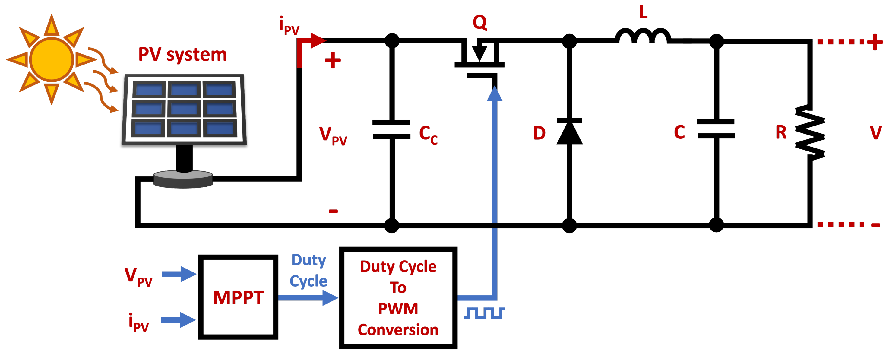
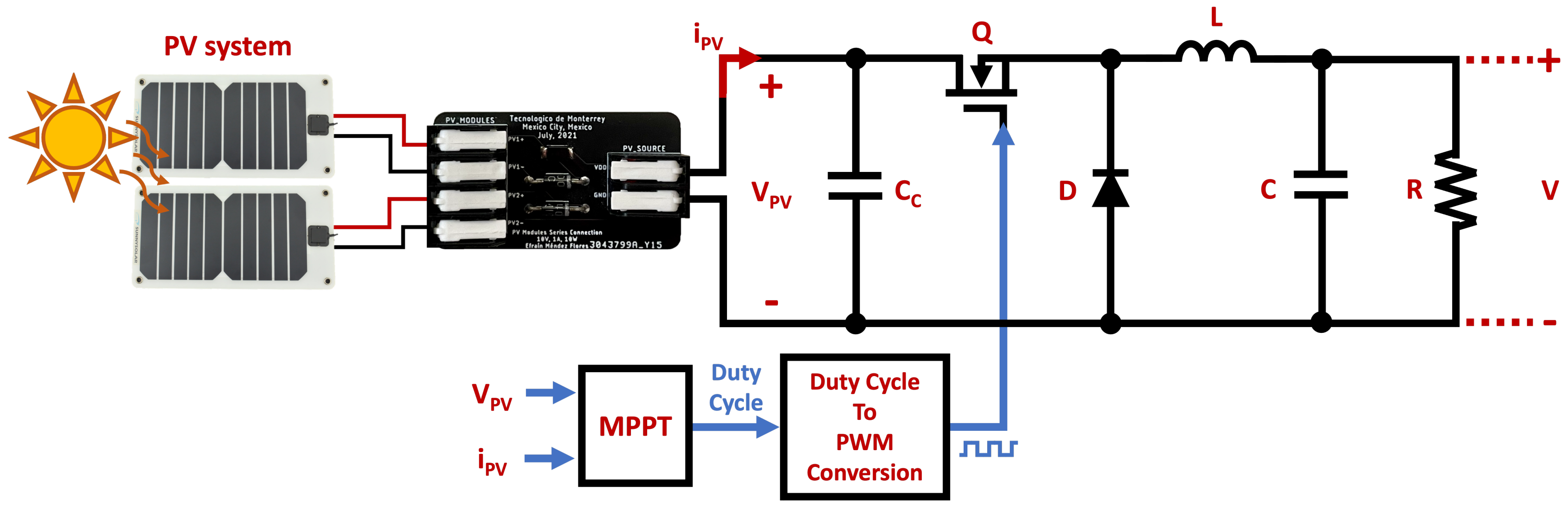
Then, to explain how the designed circuit together with the PV system are connected as the source of the DC–DC converter,
Figure 18 embeds the connections of the PV cells and the manufactured PCB from
Figure 17 into the case study topology from
Figure 13, addressing where and how the elements are interconnected on the experimental testbed.
Nevertheless, since proper validation requires fully repeatable experiments to enable other researchers to achieve and reproduce the same results, the photovoltaic system was characterized to replicate its behavior by means of the Photovoltaic Array Simulator
N8937APV, which, according to
Keysight’s datasheet in [
38], is a DC power supply with PV mode with an operating voltage range between 0 and 1500 V at a current between 0 and 30 A, which enhances dynamic simulations of the output characteristics of PV arrays under different environmental conditions such as temperature, irradiance, age, and even cell technology. Therefore,
Keysight addressed in [
38] that the equipment is particularly useful to enable quick and comprehensive tests for MPPT algorithms.
Then, to ensure proper representation of the dynamic features of the experimental PV array by its mathematical model, and also to enhance PV emulation through the
N8937APV PV array simulator, the PV array and the N8937APV were subjected to variable voltage ramp characterization through a
Keithley 2461 SourceMeter
®, which, according to
Keithley (
Tektronix company) from [
39], is optimized for characterizing and testing high-power materials, devices, and modules; the 2461 SourceMeter
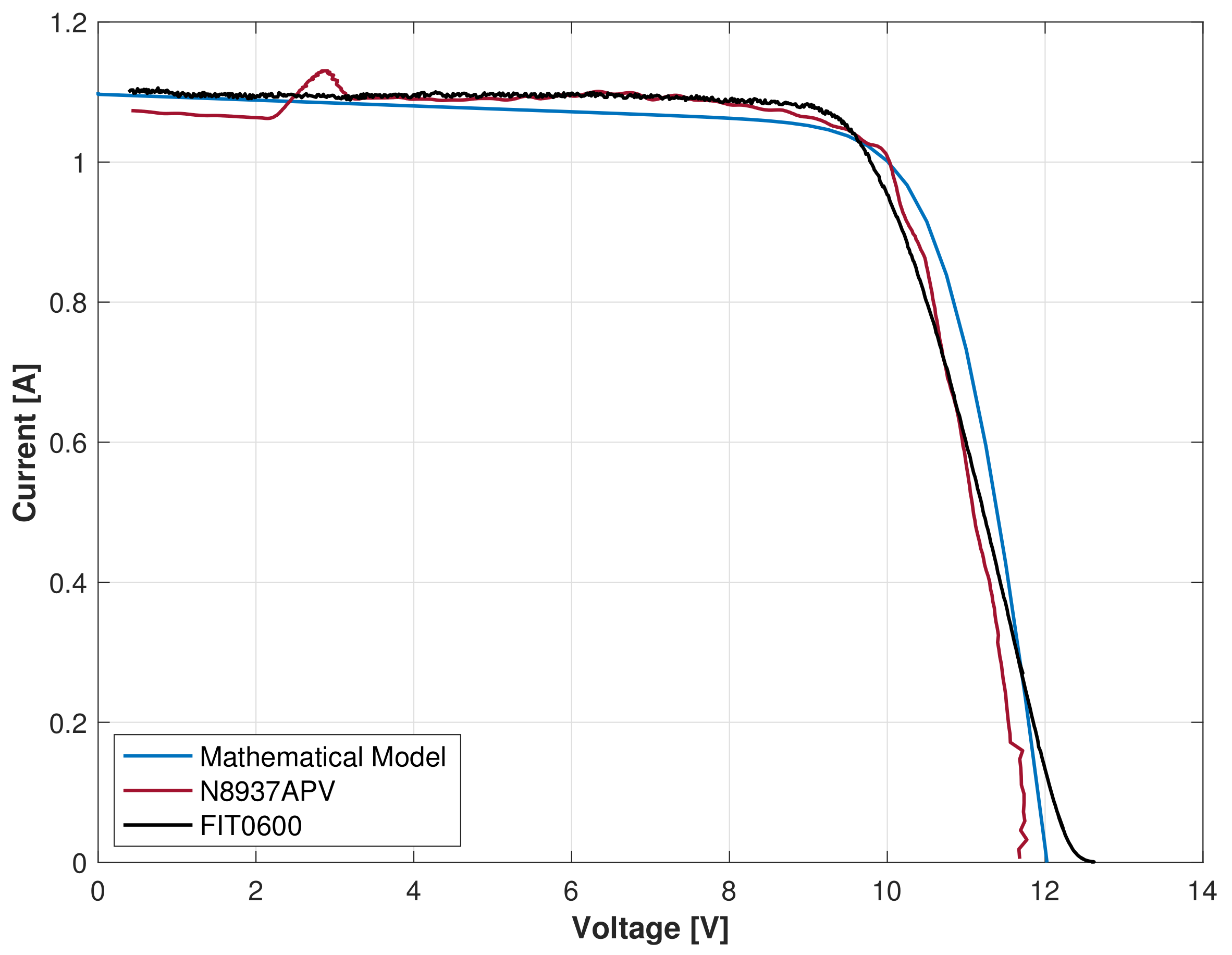
® features a 10 A/1000 W pulse current and 7 A/100 W DC current capacity. Consequently, the performed tests enabled us to obtain and compare the IV profiles of the PV arrays and the
N8937APV, which, in addition to the mathematical model profile, are presented in
Figure 19.
Consequently, we clearly validated that the IV dynamics of the mathematical model and the N8937APV are reliable representations of the dynamic features of the real FIT0600 PV array. Still, to fully address the power signal dynamic features,
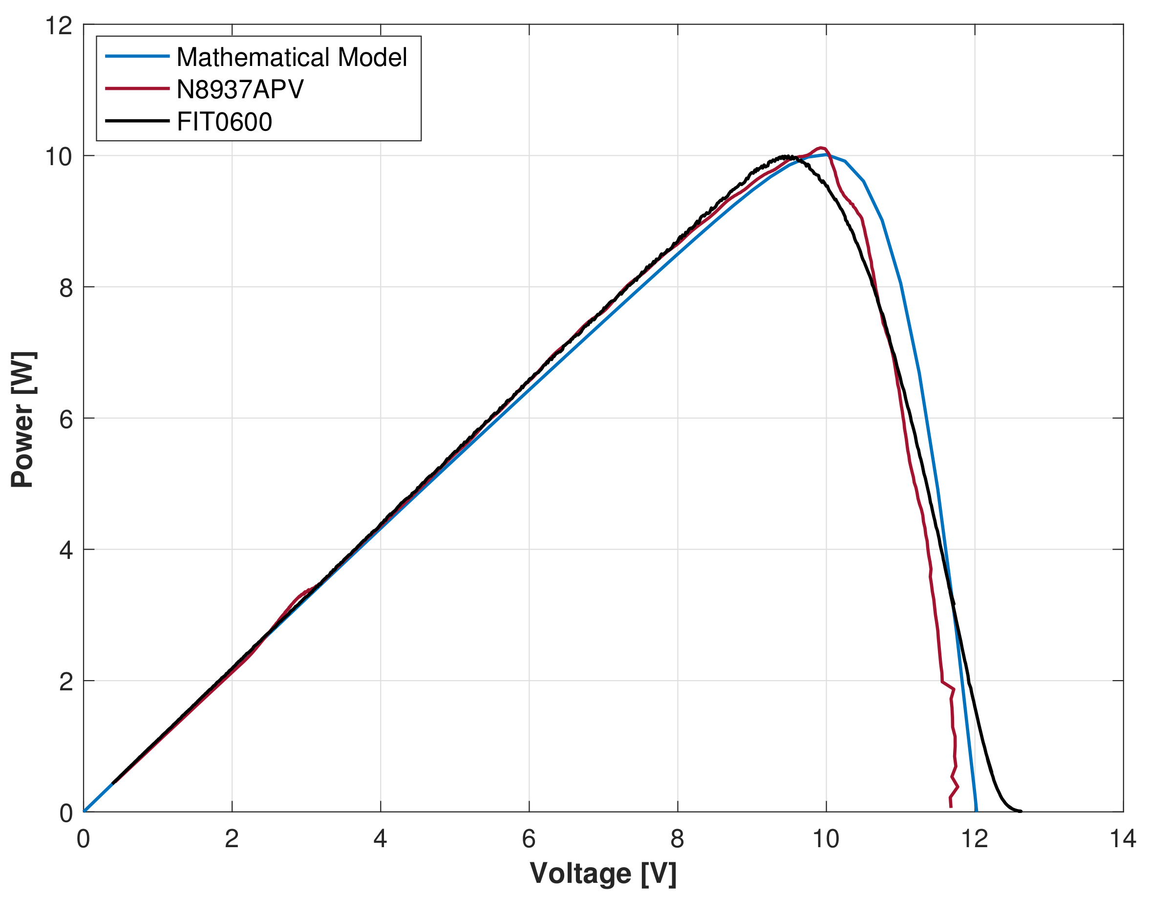
Figure 20 compares the power vs. voltage curves obtained through the acquired data from
Figure 19. Moreover,
Figure 20 allows graphical validation of the representation of the real PV array, mostly since the slopes are dynamically consistent between them, and the achievable MPP still remains around 10 W.
Furthermore, in order to sustain that the dynamics of the N8937APV and the mathematical model are valid representations of the real power behavior of the PV array, the errors and the precision of the representations against the experimental PV arrays were estimated through the quantified data; the N8937APV PV array simulator achieved 12.8089% average error that led to 87.1911% precision; meanwhile, the mathematical model compared to the experimental array achieved 84.7796% precision with an average error of 15.2204%.
Thereby, to enhance the reproducibility of the results and to ensure equal test conditions in all the experimental validation test trials, the structure presented in
Figure 18 was rearranged into the experimental topology addressed by
Figure 21, which can be inferred as valid through the dynamic comparison from
Figure 20.
Therefore, the following section details the main features of the designed DC–DC buck converter for the case study that enabled the experimental validation trials for the proposed improved EA-based MPPT algorithm.
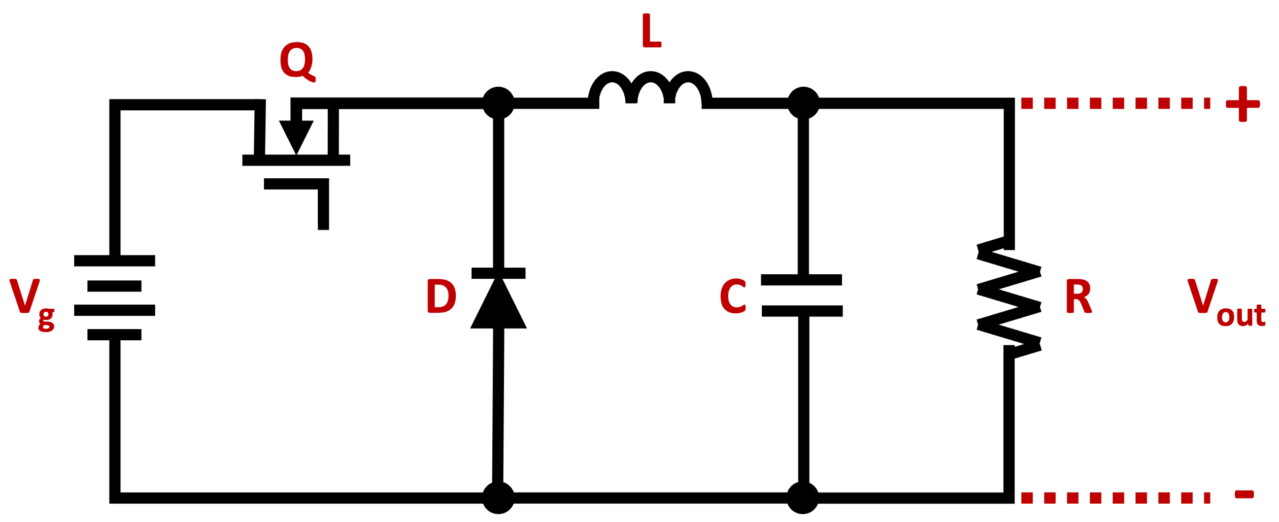
6.2. DC–DC Converter
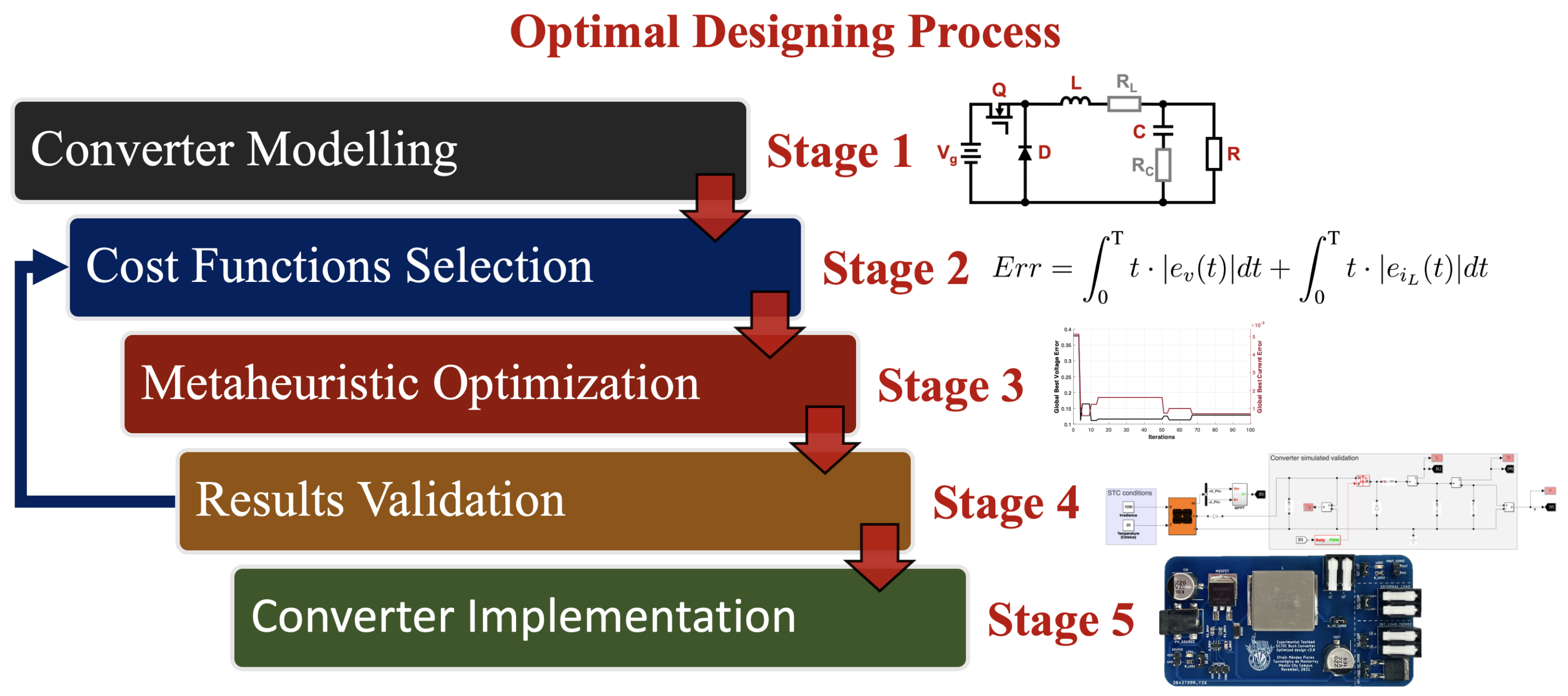
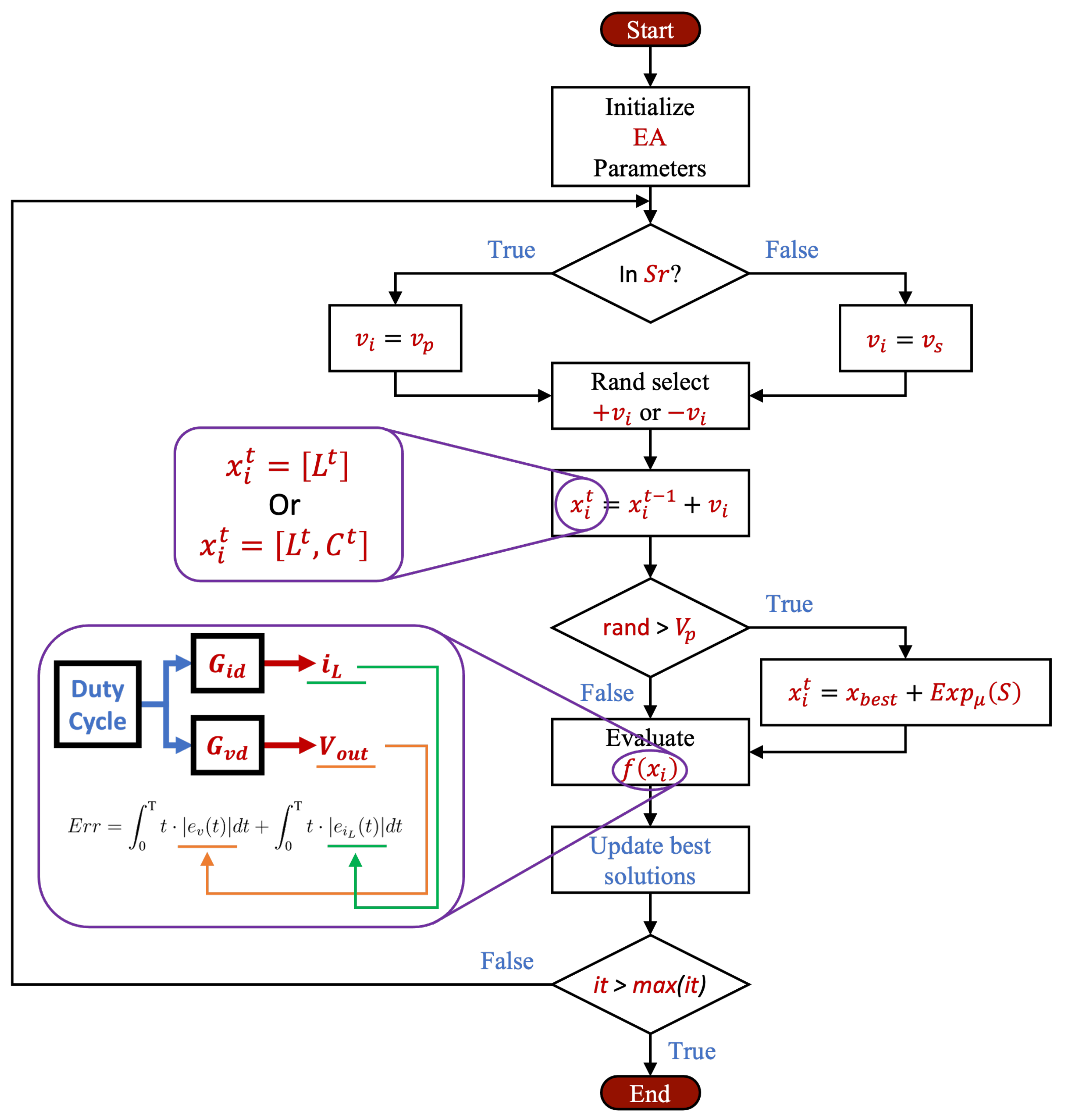
After exploring the main features of the PV source designed for experimental validation, the DC–DC converter developed for this application was developed through the optimal design methodology addressed in
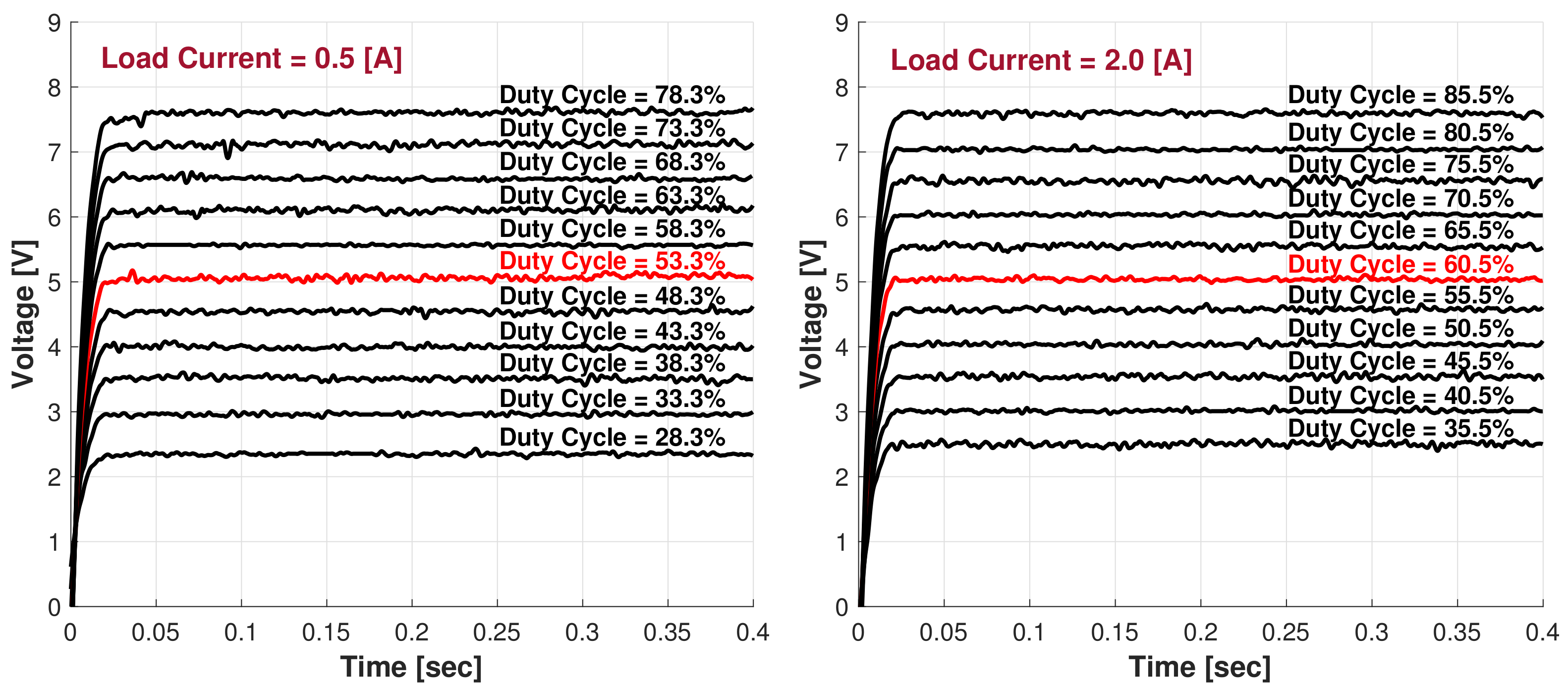
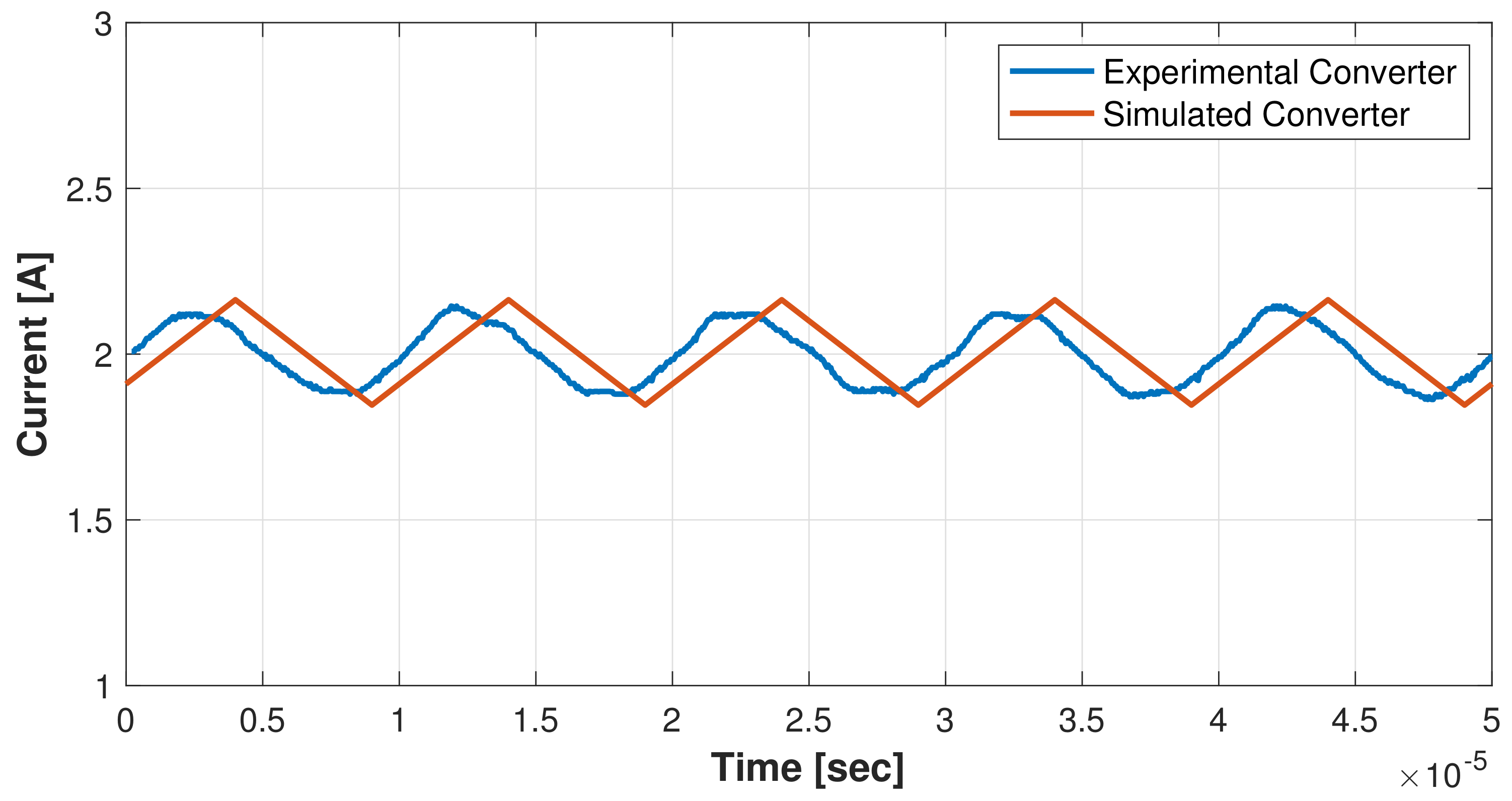
Section 5. Then, the classic EA was implemented for the design technique, where the optimization was carried out through a set of 20 epicenters (searching agents) through 100 iterations in each optimization trial (three trials), where the results were taken from the mean values among the trials; additionally, the algorithm was configured to find an inductance with low ESR, which, together with the new capacitance, could enable fast dynamic behavior while retaining low ripple-effect on the converter, which obeys the requirements of the continually induced perturbations from the MPPT algorithm.
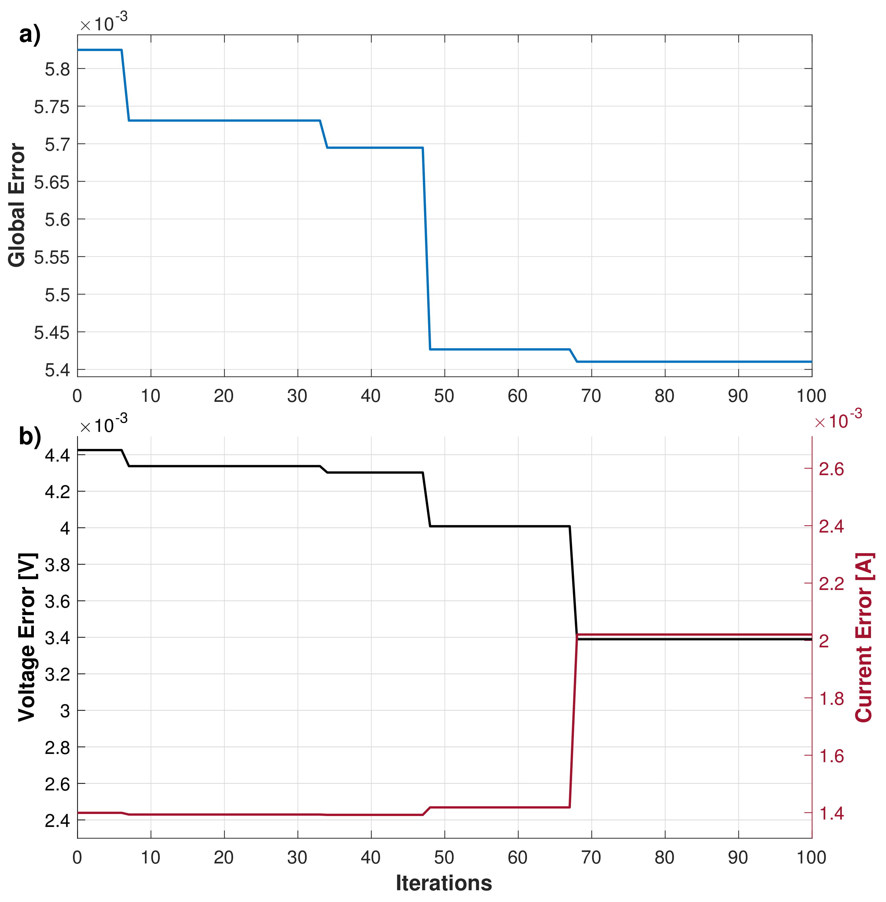
Therefore,
Figure 22 presents the convergence plots of the optimization process throughout the 100 iterations. On the one hand,
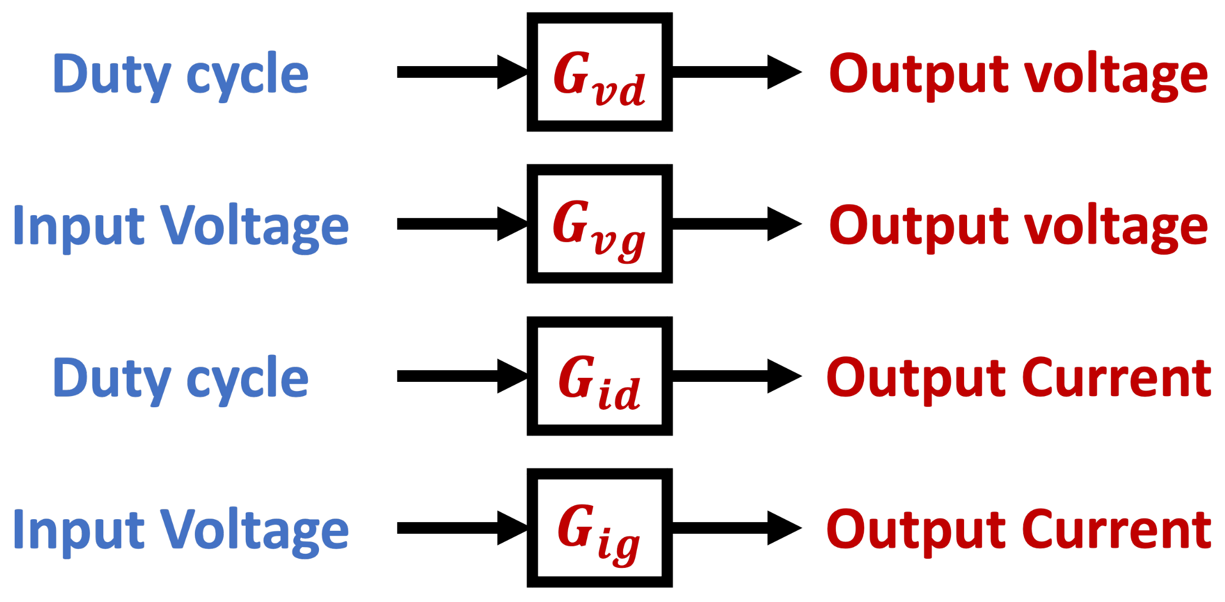
Figure 22a shows how the global error, estimated through Equation (
10), is reduced through iterations. On the other hand,
Figure 22b breaks down the global error profile into its voltage and current components, since Equation (
10) highlighted, through
and
, where the ITAE from the voltage and current errors are estimated.
Consequently, profiles from
Figure 22a,b show how multiobjective optimization enables equilibrium between the errors, where the metaheuristic algorithm finds the optimal components for which the converter has the best performance for the given application (MPPT tests in this case). Accordingly, the inductance and capacitance results optimized by the algorithm meanly settled at 79.677
H and 215.64
F, with a mean global error measured through Equation (
10) of 0.0054103 after 100 iterations (as seen in
Figure 22a).
Subsequently, the experimental capacitor and inductor were selected through study of the nearest available commercial values; thus, the selected capacitance was an aluminum organic polymer 220
F capacitor. Meanwhile, to meet the dynamics and efficiency requirements of the application, the inductance was taken as a fixed-shielded high-current molded 82
H power inductor. Then, the main parameters from the selected inductor are presented in
Table 3,
Table 4 presents the main parameters of the selected capacitor for the circuit, and
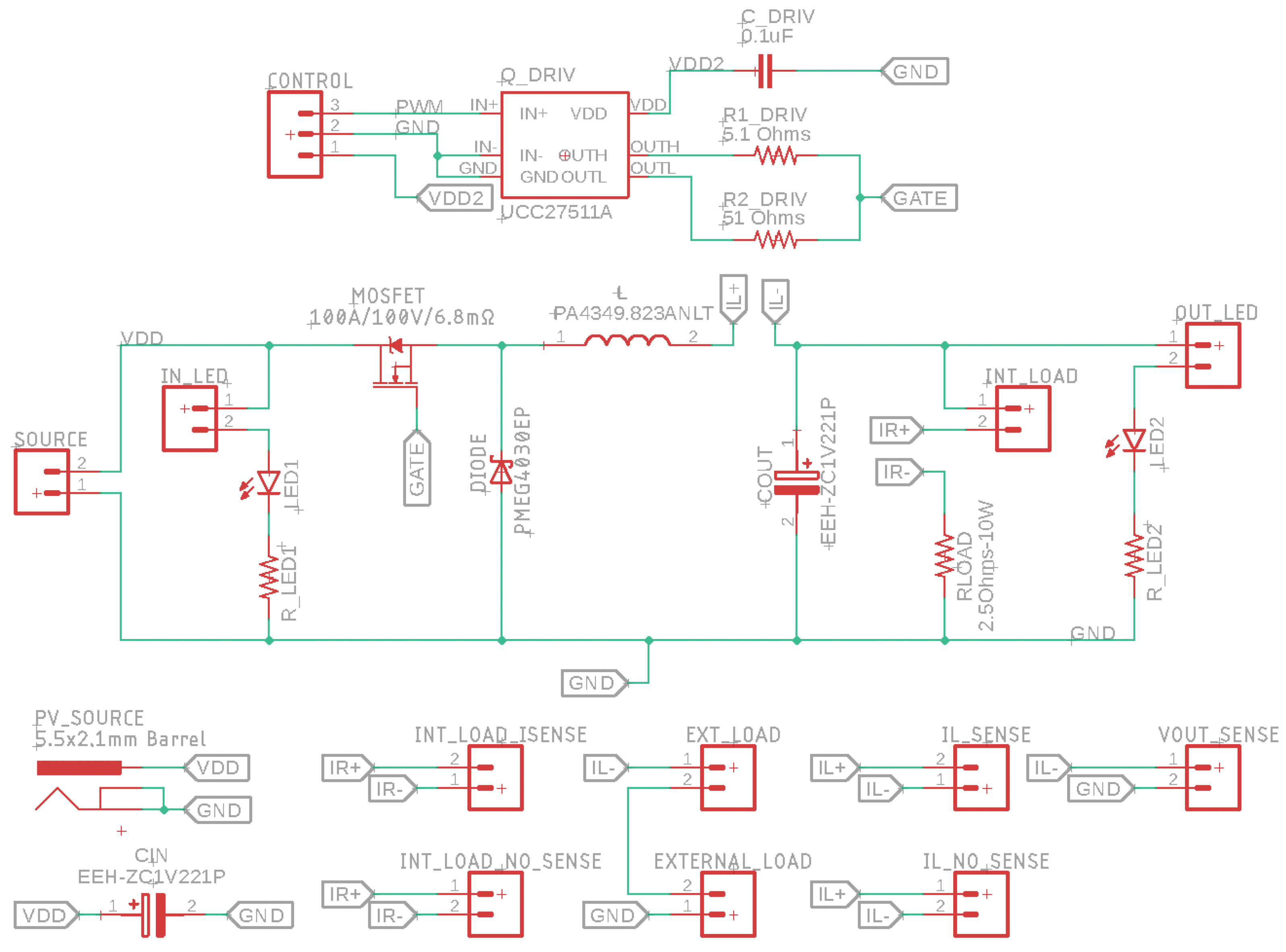
Figure 23 shows the schematics diagram of the circuit and where the capacitance and the inductance were implemented.
Additionally,
Figure 23, shows at the top the required connections for the MOSFET’s gate driver, which was selected to be the single-channel gate driver UCC27511A, as also addressed in the experimental implementation presented by Mendez-Flores, E., et al. in [
29]; since according to the datasheet presented by Texas instruments in [
42], it is a compact, high-speed solution suitable for DC–DC converters and also provides parasitic Miller turn-on effect rejection.
Moreover, in the middle of
Figure 23, the main structure of the designed DC–DC converter is presented; the figure also presents how the input and output LED indicators can be decoupled from the system in order to enhance the possibility of tests through the minimal required components without the case apart when fast input/output verification is required.
Additionally, two different PV source connections were added to the design; on the one hand,
mm barrel was provided as an additional safety measure, which allows the user to avoid the possible scenario where the PV source is mistakenly connected with reversed polarity. On the other hand, source header pins were also provided on the design to enable tests with additional fixed sources, thus, both headers enable a suitable option for a different external sources for the system. The CIN capacitor below the barrel jack is the coupling capacitor previously described in
Figure 18, the capacitance of which is the same as the output capacitance described in
Table 4.
Hence, from the bottom of
Figure 23, the two-pin connectors provide reconfiguration options for the converter; if both INT_LOAD_NO_SENSE connectors are joined, the INT_LOAD_SENSE terminals are useless since those terminals are bridged, but if they are not bridged, INT_LOAD_SENSE can be used to connect a current sensor to monitor the current through the internal load of the circuit. Still, the internal load (2.5
) can be removed from the test trials if the INT_LOAD terminals are detached.
Similarly, if the EXT_LOAD headers are bridged and the INT_LOAD terminals are separated, an external load can be attached to the converter to enable tests under different load experiments; therefore, the external can be connected and monitored through the EXTERNAL_LOAD terminals. Finally, when the IL_NO_SENSE terminals are not united, the current through the inductance can be monitored through an external sensor at the IL_SENSE terminals.
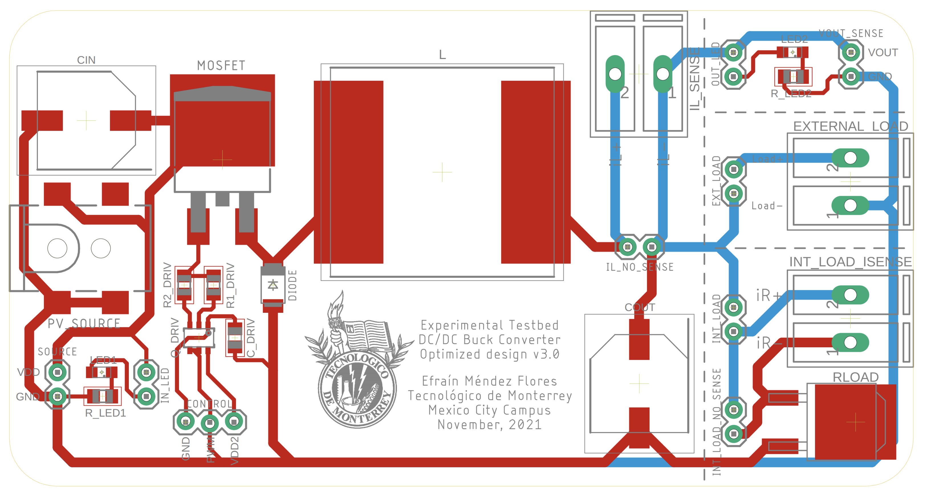
Thereby, under those circumstances and with those design considerations in mind,
Figure 24 presents the PCB layout designed for the DC–DC converter implementation for the PV experimental case study, where all the elements from
Figure 23 were arranged and routed for the manufacturing stage of the converter. Then,
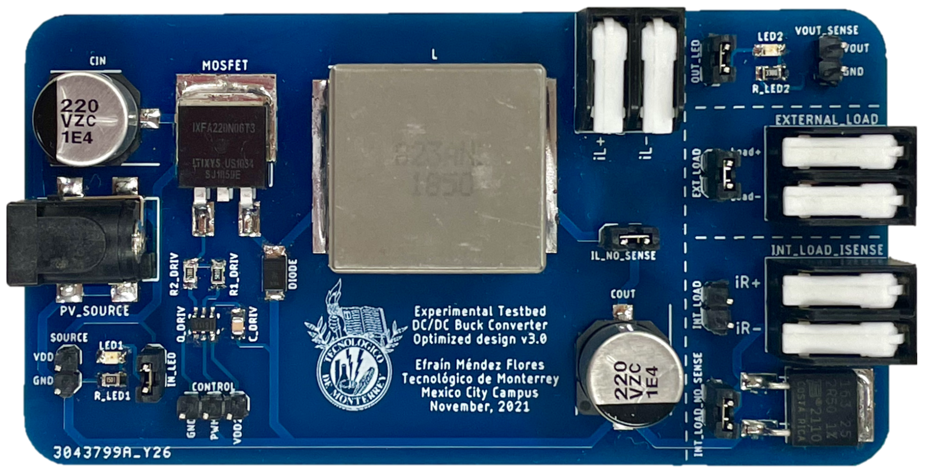
Figure 25 presents the manufactured PCB of the DC–DC converter.
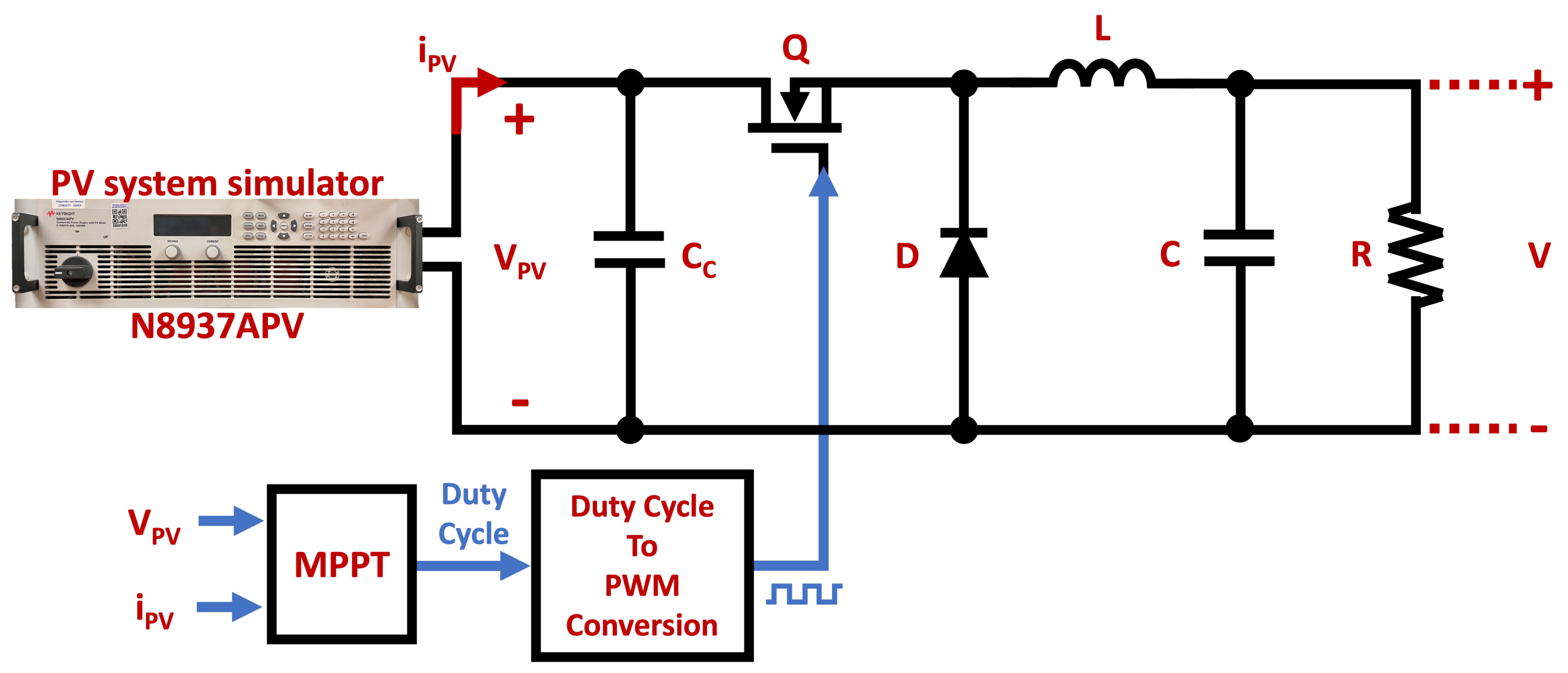
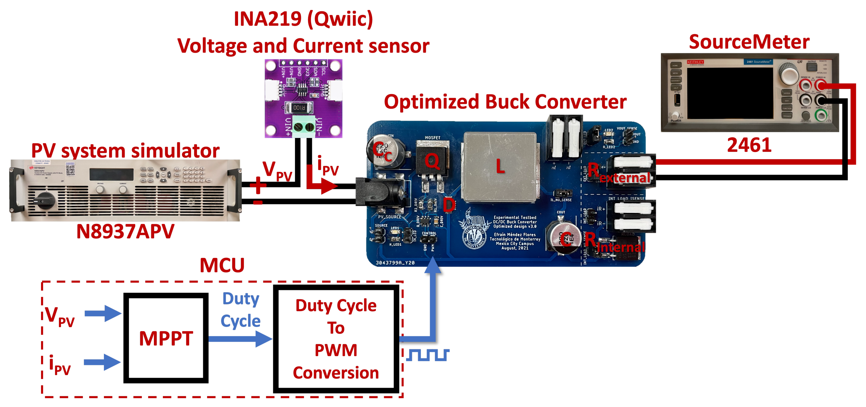
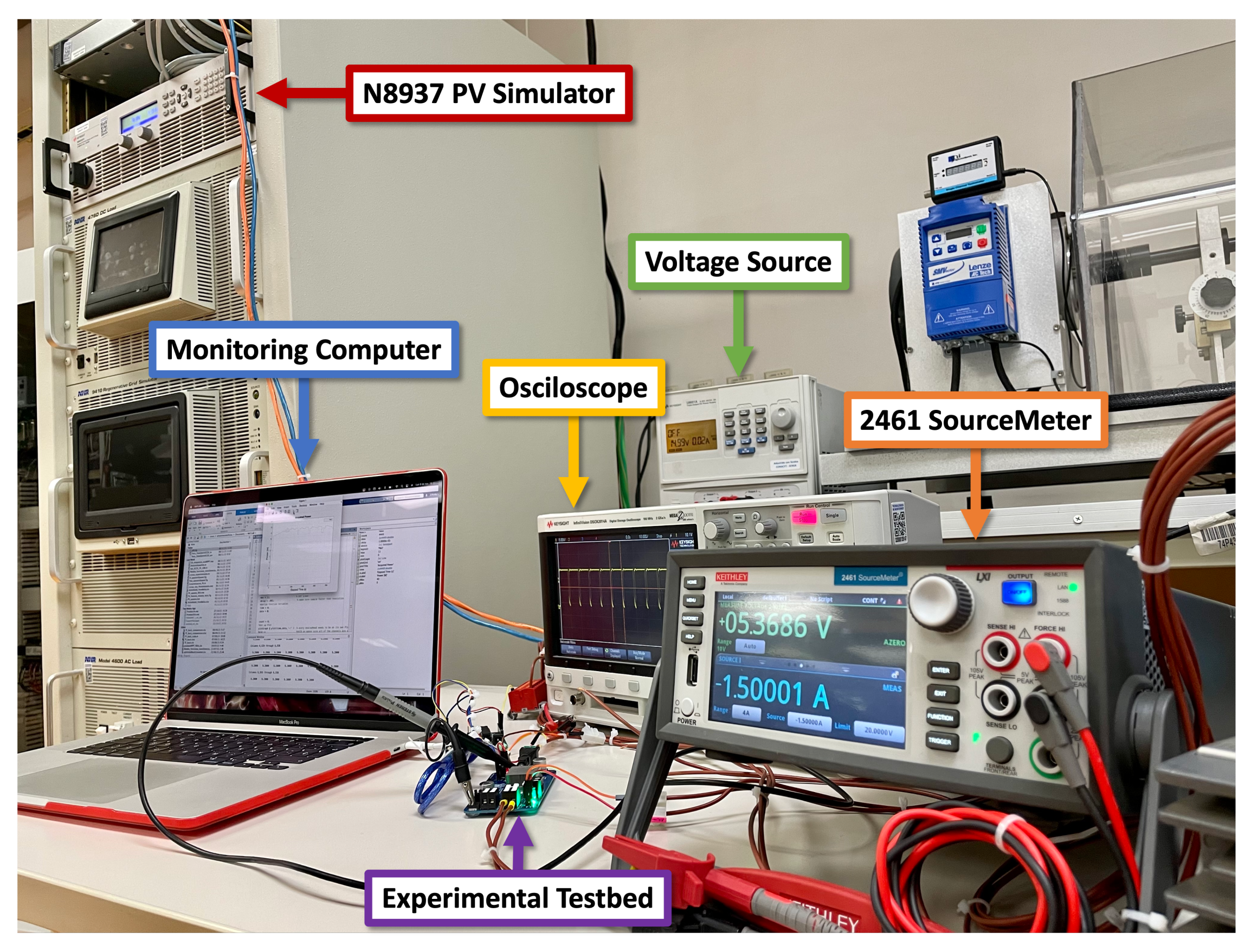
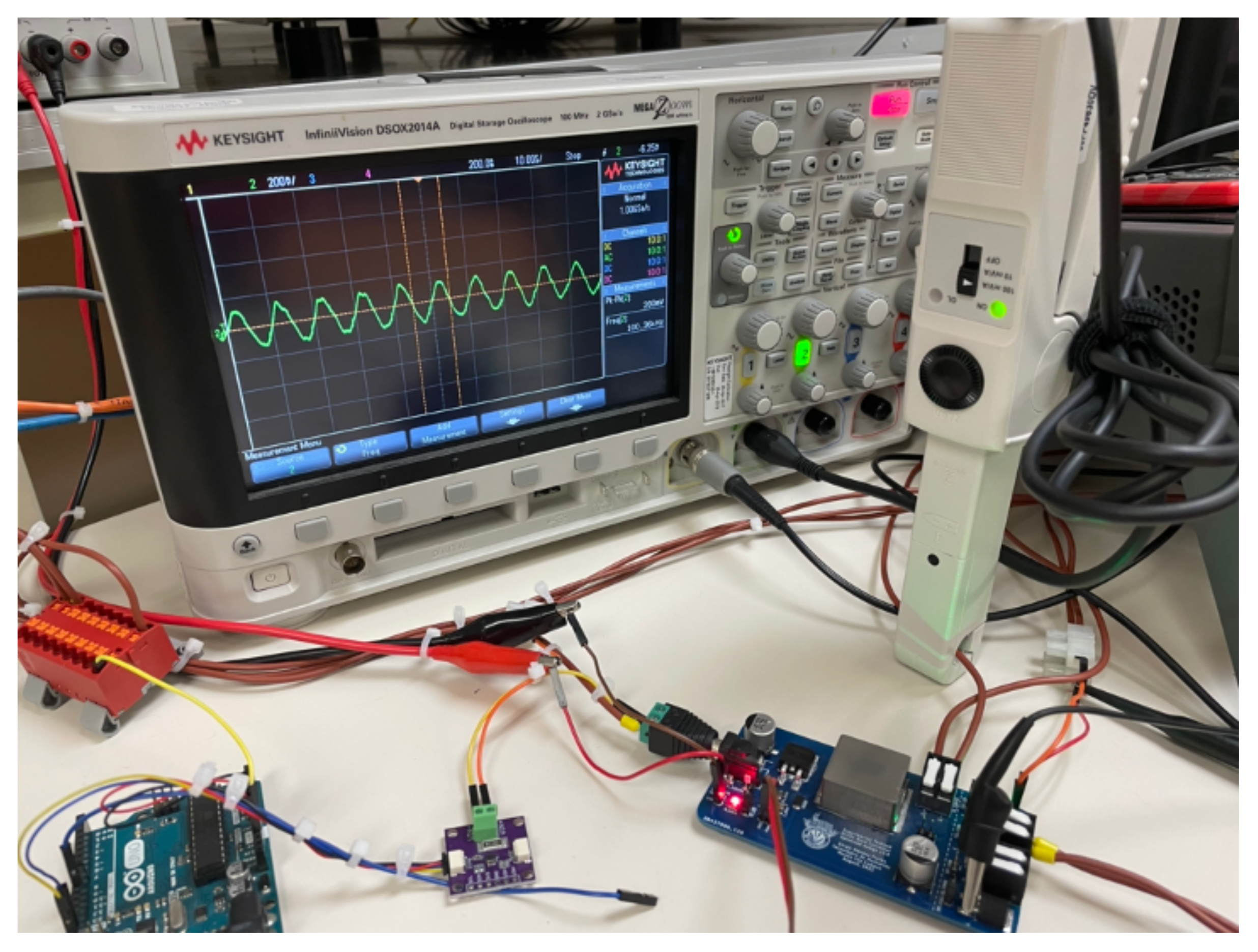
Hence, keeping up with the figure sequence that shows how the experimental frame was built for the validations tests,
Figure 26 presents the case study topology, where integration of the N8937APV PV array simulator, the 2461 SourceMeter
®, and the optimized buck converter (from
Figure 25) is presented. Additionally, from
Figure 26, it can be seen where the main elements and variables from
Figure 13 are implemented; also
Figure 26 highlights the MPPT and the PWM stages, addressing where the microcontroller unit (MCU) acquires and processes the data to provide the control signal to the system.
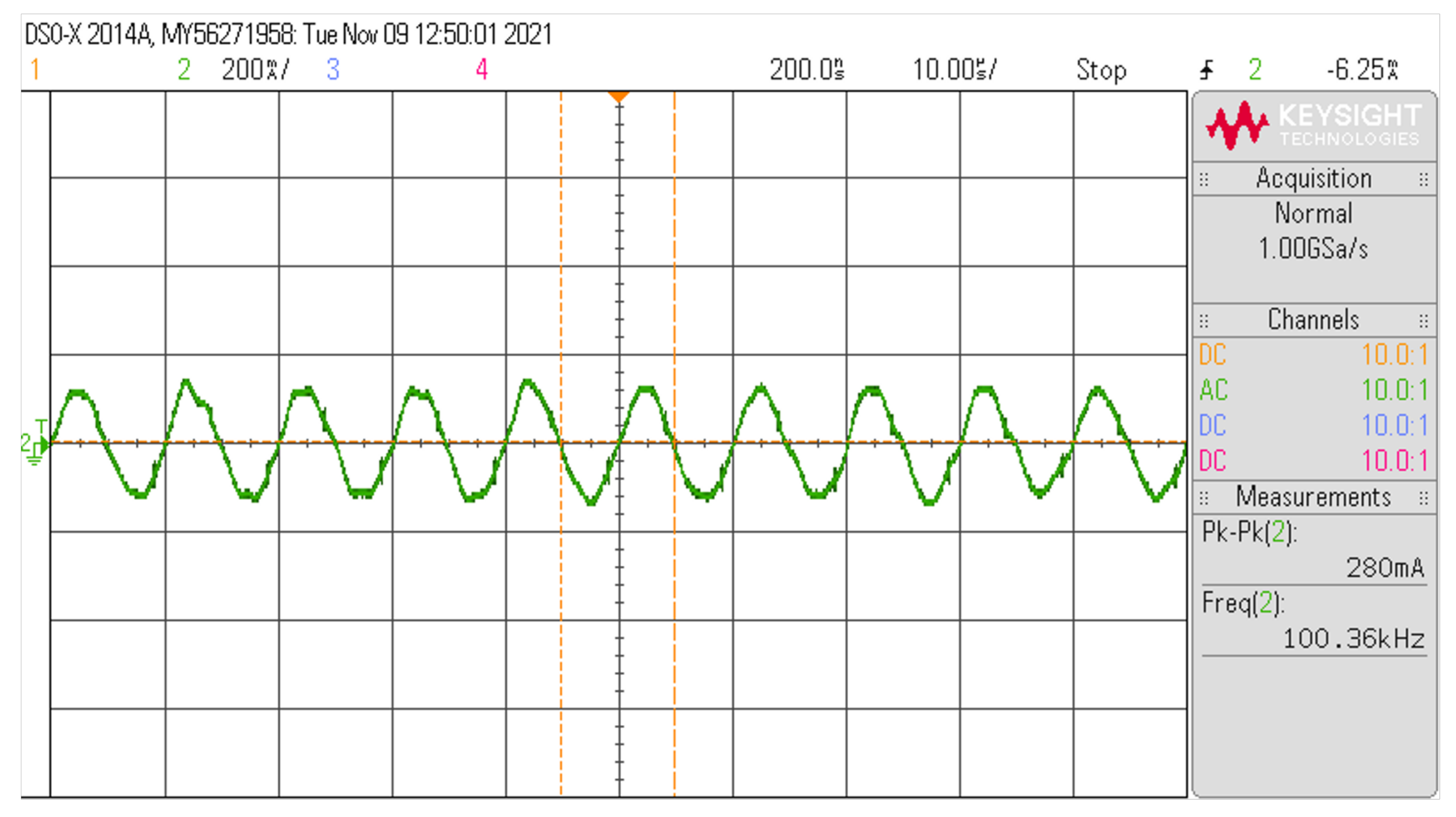
Yet it is critical to mention that from now on, the data acquisition process regarding the voltage, current, and power signals for the implementation and evaluation of the proposed MPPT algorithm are carried out through the INA219 (Qwiic) module, which is based on the INA219 power monitor with I
C interface presented by Texas Instruments in [
43]. Then, Qwiic is a rapid prototyping standard developed by Sparkfun
® that uses 4-pin JST connectors to quickly interface development boards with sensors, microcontrollers, and displays, among others things.
The INA219 (Qwiic) module was selected for the experimental tests since the module provides a reliable solution that reports current, voltage, and power through I
C protocol with up to 1% precision, suitable for tracking solar power generation applications. According to [
43] by Texas Instruments, the sensor can measure voltage up to 26 V and current up to 3.2 A, which fits on the 10 W case study proposed to work at 10 V and 1 A at the PV terminals.
Consequently,
Table 5 summarizes the parameters of the buck converter for which its design was optimized for the PV case study. Nevertheless, since the novel optimal design methodology validated by Mendez-Flores, E., et al. in [
29] is acknowledged as one of the main contributions of this work, the dynamic performance profiles of the experimental converter through multiple duty-cycle step signals are provided in the following section of this work as part of the featured results.
Therefore, the following section presents the main results of the experimental integration case study proposed to validate how the contributions of this work enhance smarter photovoltaic systems. Then, among the results from the following section, it is seen how the dynamic features of the optimized converter enable a prominent testbed for the algorithm’s validation.


