Structural, Optical and Electrical Properties of HfO2 Thin Films Deposited at Low-Temperature Using Plasma-Enhanced Atomic Layer Deposition


Abstract
:1. Introduction
2. Materials and Methods
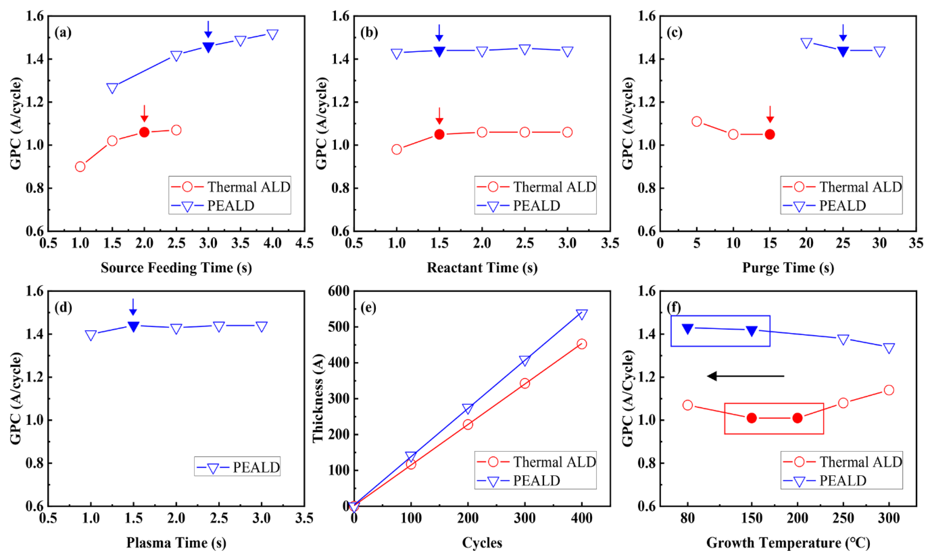
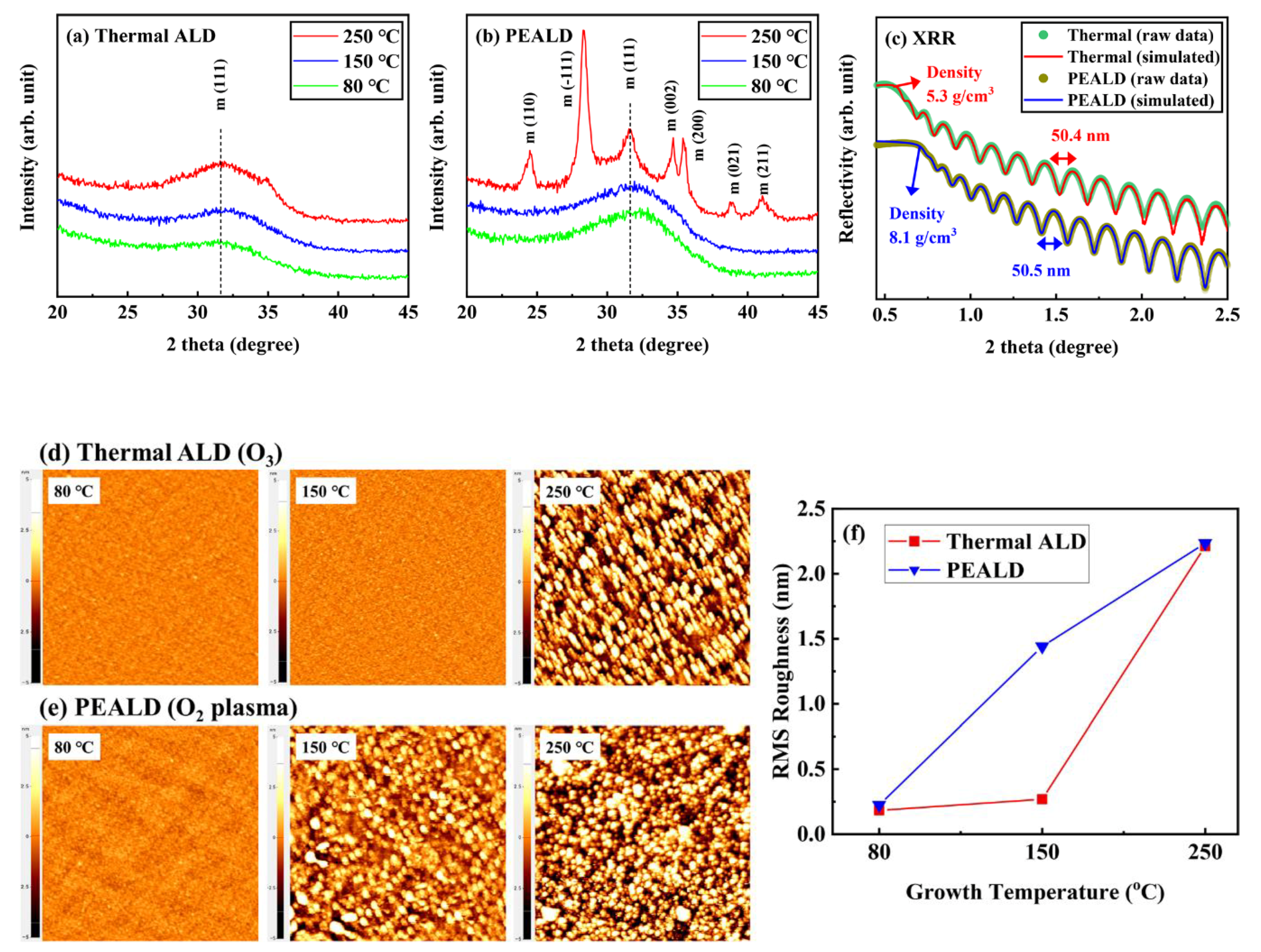
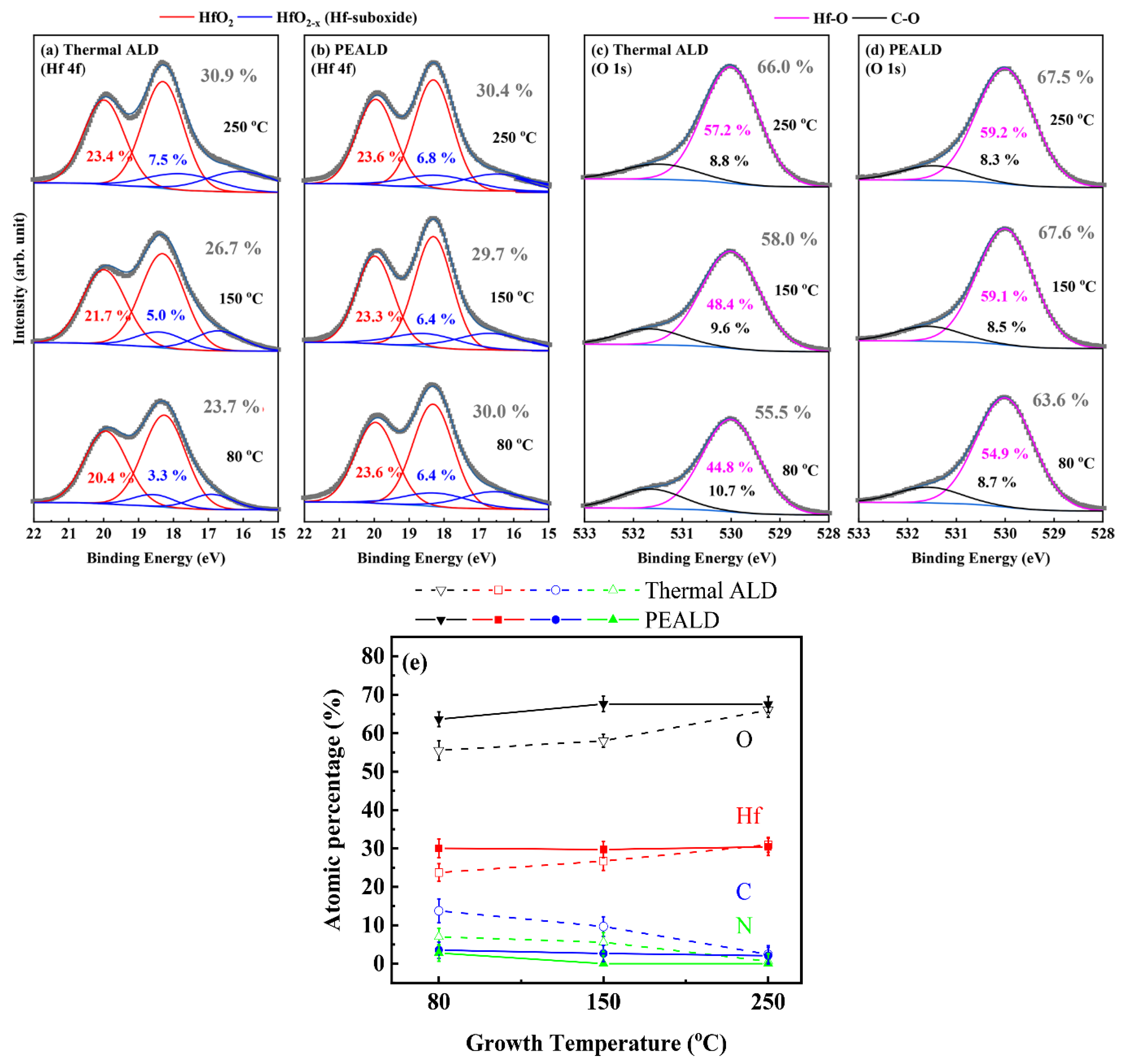
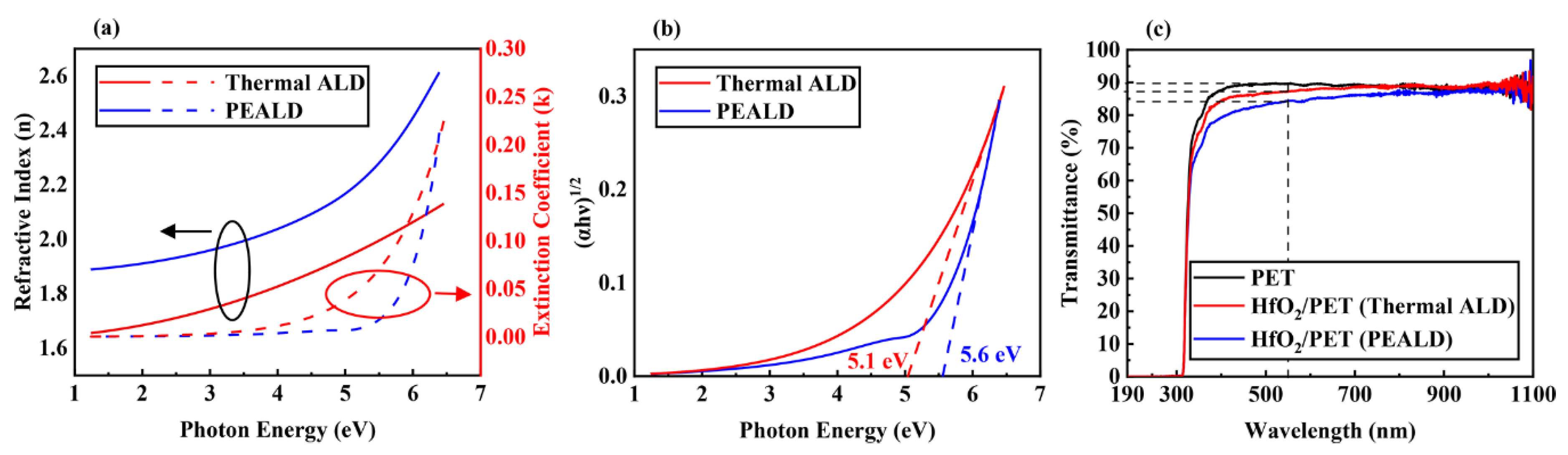
3. Results and Discussion
4. Conclusions
Author Contributions
Funding
Conflicts of Interest
References
- Masuda, H.; Nakai, M.; Kubo, M. Characteristics and limitation of scaled-down MOSFET’s due to two-dimensional field effect. IEEE Trans. Electron Devices 1979, 26, 980–986. [Google Scholar] [CrossRef]
- Han, D.; Kang, J.; Lin, C.; Han, R. Reliability characteristics of high-K gate dielectrics HfO2 in metal-oxide semiconductor capacitors. Microelectron. Eng. 2003, 66, 643–647. [Google Scholar] [CrossRef]
- Gusev, E.P.; D’Emic, C.P. Charge detrapping in HfO2 high-κ gate dielectric stacks. Appl. Phys. Lett. 2003, 83, 5223–5225. [Google Scholar] [CrossRef]
- Nakajima, K.; Joumori, S.; Suzuki, M.; Kimura, K.; Osipowicz, T.; Tok, K.L.; Zheng, J.Z.; See, A.; Zhang, B.C. Strain profiling of HfO2/Si(001) interface with high-resolution Rutherford backscattering spectroscopy. Appl. Phys. Lett. 2003, 83, 296–298. [Google Scholar] [CrossRef] [Green Version]
- An, J.-K.; Chung, N.-K.; Kim, J.-T.; Hahm, S.-H.; Lee, G.; Lee, S.; Lee, T.; Park, I.-S.; Yun, J.-Y. Effect of Growth Temperature on the Structural and Electrical Properties of ZrO2 Films Fabricated by Atomic Layer Deposition Using a CpZr[N(CH3)2]3/C7H8 Cocktail Precursor. Materials 2018, 11, 386. [Google Scholar] [CrossRef] [PubMed] [Green Version]
- He, W. ALD: Atomic Layer Deposition—Precise and Conformal Coating for Better Performance. In Handbook of Manufacturing Engineering and Technology; Springer: London, UK, 2015; pp. 2959–2996. ISBN 9781447146704. [Google Scholar]
- Johnson, R.W.; Hultqvist, A.; Bent, S.F. A brief review of atomic layer deposition: From fundamentals to applications. Mater. Today 2014, 17, 236–246. [Google Scholar] [CrossRef]
- Vähä-Nissi, M.; Pitkänen, M.; Salo, E.; Sievänen-Rahijärvi, J.; Putkonen, M.; Harlin, A. Atomic layer deposited thin barrier films for packaging. Cellul. Chem. Technol. 2015, 49, 575–585. [Google Scholar]
- Zou, M.; Ma, Y.; Yuan, X.; Hu, Y.; Liu, J.; Jin, Z. Flexible devices: From materials, architectures to applications. J. Semicond. 2018, 39, 011010. [Google Scholar] [CrossRef]
- Huang, S.; Liu, Y.; Zhao, Y.; Ren, Z.; Guo, C.F. Flexible Electronics: Stretchable Electrodes and Their Future. Adv. Funct. Mater. 2019, 29, 1805924. [Google Scholar] [CrossRef]
- Oh, N.K.; Kim, J.-T.; Ahn, J.-K.; Kang, G.; Kim, S.Y.; Yun, J.-Y. The Effects of Thermal Decomposition of Tetrakis-ethylmethylaminohafnium (TEMAHf) Precursors on HfO2 Film Growth using Atomic Layer Deposition. Appl. Sci. Converg. Technol. 2016, 25, 56–60. [Google Scholar] [CrossRef]
- Niu, G.; Kim, H.-D.; Roelofs, R.; Perez, E.; Schubert, M.A.; Zaumseil, P.; Costina, I.; Wenger, C. Material insights of HfO2-based integrated 1-transistor-1-resistor resistive random access memory devices processed by batch atomic layer deposition. Sci. Rep. 2016, 6, 28155. [Google Scholar] [CrossRef] [PubMed] [Green Version]
- Fan, J.; Liu, H.; Kuang, Q.; Gao, B.; Ma, F.; Hao, Y. Physical properties and electrical characteristics of H2O-based and O3-based HfO2 films deposited by ALD. Microelectron. Reliab. 2012, 52, 1043–1049. [Google Scholar] [CrossRef]
- Kim, J.H.; Park, T.J.; Kim, S.K.; Cho, D.-Y.; Jung, H.-S.; Lee, S.Y.; Hwang, C.S. Chemical structures and electrical properties of atomic layer deposited HfO2 thin films grown at an extremely low temperature (≤ 100 °C) using O3 as an oxygen source. Appl. Surf. Sci. 2014, 292, 852–856. [Google Scholar] [CrossRef]
- Richter, C.; Schenk, T.; Schroeder, U.; Mikolajick, T. Film properties of low temperature HfO2 grown with H2O, O3, or remote O2 -plasma. J. Vac. Sci. Technol. A Vac. Surf. Film. 2014, 32, 01A117. [Google Scholar] [CrossRef]
- Xiao, Z.; Kisslinger, K.; Chance, S.; Banks, S. Comparison of Hafnium Dioxide and Zirconium Dioxide Grown by Plasma-Enhanced Atomic Layer Deposition for the Application of Electronic Materials. Crystals 2020, 10, 136. [Google Scholar] [CrossRef] [Green Version]
- Chen, Z.; Wang, H.; Wang, X.; Chen, P.; Liu, Y.; Zhao, H.; Zhao, Y.; Duan, Y. Low-temperature remote plasma enhanced atomic layer deposition of ZrO2/zircone nanolaminate film for efficient encapsulation of flexible organic light-emitting diodes. Sci. Rep. 2017, 7, 1–9. [Google Scholar] [CrossRef] [Green Version]
- Barrera-Díaz, C.; Cañizares, P.; Fernández, F.J.; Natividad, R.; Rodrigo, M.A. Electrochemical Advanced Oxidation Processes: An Overview of the Current Applications to Actual Industrial Effluents. J. Mex. Chem. Soc. 2017, 58, 256–275. [Google Scholar] [CrossRef] [Green Version]
- Poyatos, J.M.; Muñio, M.M.; Almecija, M.C.; Torres, J.C.; Hontoria, E.; Osorio, F. Advanced Oxidation Processes for Wastewater Treatment: State of the Art. Water. Air. Soil Pollut. 2010, 205, 187–204. [Google Scholar] [CrossRef]
- Rodríguez, A.; Rosal, R.; Perdigón-Melón, J.A.; Mezcua, M.; Agüera, A.; Hernando, M.D.; Letón, P.; Fernández-Alba, A.R.; García-Calvo, E. Ozone-Based Technologies in Water and Wastewater Treatment. In Emerging Contaminants from Industrial and Municipal Waste; Springer: Berlin/Heidelberg, Germany, 2008; pp. 127–175. ISBN 9783540792093. [Google Scholar]
- Profijt, H.B.; Potts, S.E.; van de Sanden, M.C.M.; Kessels, W.M.M. Plasma-Assisted Atomic Layer Deposition: Basics, Opportunities, and Challenges. J. Vac. Sci. Technol. A Vac. Surf. Film. 2011, 29, 050801. [Google Scholar] [CrossRef] [Green Version]
- Provine, J.; Schindler, P.; Torgersen, J.; Kim, H.J.; Karnthaler, H.-P.; Prinz, F.B. Atomic layer deposition by reaction of molecular oxygen with tetrakisdimethylamido-metal precursors. J. Vac. Sci. Technol. A Vac. Surf. Film. 2016, 34, 01A138. [Google Scholar] [CrossRef] [Green Version]
- Fang, G.Y.; Xu, L.N.; Cao, Y.Q.; Wang, L.G.; Wu, D.; Li, A.D. Self-catalysis by aminosilanes and strong surface oxidation by O2 plasma in plasma-enhanced atomic layer deposition of high-quality SiO2. Chem. Commun. 2015, 51, 1341–1344. [Google Scholar] [CrossRef] [PubMed]
- Becker, M.; Sierka, M. Atomistic simulations of plasma-enhanced atomic layer deposition. Materials 2019, 12, 2605. [Google Scholar] [CrossRef] [PubMed] [Green Version]
- Hoflund, G.B. Application of novel O- and H-atom sources in molecular beam epitaxy. J. Vac. Sci. Technol. B Microelectron. Nanom. Struct. 1998, 16, 1446. [Google Scholar] [CrossRef]
- Khanuja, M.; Sharma, H.; Mehta, B.R.; Shivaprasad, S.M. XPS depth-profile of the suboxide distribution at the native oxide/Ta interface. J. Electron Spectros. Relat. Phenom. 2009, 169, 41–45. [Google Scholar] [CrossRef]
- Knoops, H.C.M.; Potts, S.E.; Bol, A.A.; Kessels, W.M.M. Atomic Layer Deposition. In Handbook of Crystal Growth; Elsevier: Amsterdam, The Netherlands, 2015; pp. 1101–1134. ISBN 9780444633040. [Google Scholar]
- Chae, H.; Sawin, H.H. Plasma Kinetic Study of Silicon-Dioxide Removal with Fluorocompounds in a Plasma-Enhanced Chemical Vapor Deposition Chamber. J. Korean Phys. Soc. 2007, 51, 978. [Google Scholar] [CrossRef]
- Cho, D.-Y.; Jung, H.S.; Yu, I.-H.; Yoon, J.H.; Kim, H.K.; Lee, S.Y.; Jeon, S.H.; Han, S.; Kim, J.H.; Park, T.J.; et al. Stabilization of Tetragonal HfO2 under Low Active Oxygen Source Environment in Atomic Layer Deposition. Chem. Mater. 2012, 24, 3534–3543. [Google Scholar] [CrossRef]
- Kondaiah, P.; Shaik, H.; Mohan Rao, G. Studies on RF magnetron sputtered HfO2 thin films for microelectronic applications. Electron. Mater. Lett. 2015, 11, 592–600. [Google Scholar] [CrossRef]
- Luo, X.; Li, Y.; Yang, H.; Liang, Y.; He, K.; Sun, W.; Lin, H.-H.; Yao, S.; Lu, X.; Wan, L.; et al. Investigation of HfO2 Thin Films on Si by X-ray Photoelectron Spectroscopy, Rutherford Backscattering, Grazing Incidence X-ray Diffraction and Variable Angle Spectroscopic Ellipsometry. Crystals 2018, 8, 248. [Google Scholar] [CrossRef] [Green Version]
- Blaschke, D.; Munnik, F.; Grenzer, J.; Rebohle, L.; Schmidt, H.; Zahn, P.; Gemming, S. A correlation study of layer growth rate, thickness uniformity, stoichiometry, and hydrogen impurity level in HfO2 thin films grown by ALD between 100 °C and 350 °C. Appl. Surf. Sci. 2020, 506, 144188. [Google Scholar] [CrossRef]
- Chourasia, A.R.; Hickman, J.L.; Miller, R.L.; Nixon, G.A.; Seabolt, M.A. X-Ray Photoemission Study of the Oxidation of Hafnium. Int. J. Spectrosc. 2009, 2009, 1–6. [Google Scholar] [CrossRef] [Green Version]
- Sopori, B.; Rupnowski, P.; Shet, S.; Budhraja, V.; Call, N.; Johnston, S.; Seacrist, M.; Shi, G.; Chen, J.; Deshpande, A. Influence of defects and defect distributions in multicrystalline silicon on solar cell performance. In Proceedings of the 35th IEEE Photovoltaic Specialists Conference, Honolulu, HI, USA, 20–25 June 2010. [Google Scholar]
- Coufová, P.; Novák, J.; Hlasivcová, N. Hydroxyl as a Defect of the Perovskite BaTiO3 Lattice. J. Chem. Phys. 1966, 45, 3171–3174. [Google Scholar] [CrossRef]
- Cho, Y.J.; Nguyen, N.V.; Richter, C.A.; Ehrstein, J.R.; Lee, B.H.; Lee, J.C. Spectroscopic ellipsometry characterization of high- k dielectric HfO2 thin films and the high-temperature annealing effects on their optical properties. Appl. Phys. Lett. 2002, 80, 1249–1251. [Google Scholar] [CrossRef] [Green Version]
- Nam, T.; Park, Y.J.; Lee, H.; Oh, I.-K.; Ahn, J.-H.; Cho, S.M.; Kim, H.; Lee, H.-B.-R. A composite layer of atomic-layer-deposited Al2O3 and graphene for flexible moisture barrier. Carbon N. Y. 2017, 116, 553–561. [Google Scholar] [CrossRef]
- Hu, B.; Yao, M.; Xiao, R.; Chen, J.; Yao, X. Optical properties of amorphous Al2O3 thin films prepared by a sol–gel process. Ceram. Int. 2014, 40, 14133–14139. [Google Scholar] [CrossRef]
- Cheynet, M.C.; Pokrant, S.; Tichelaar, F.D.; Rouvière, J.-L. Crystal structure and band gap determination of HfO2 thin films. J. Appl. Phys. 2007, 101, 054101. [Google Scholar] [CrossRef] [Green Version]
- Liu, C.; Chor, E.F.; Tan, L.S. Enhanced device performance of AlGaN/GaN HEMTs using HfO2 high- k dielectric for surface passivation and gate oxide. Semicond. Sci. Technol. 2007, 22, 522–527. [Google Scholar] [CrossRef]
- Viezbicke, B.D.; Patel, S.; Davis, B.E.; Birnie, D.P. Evaluation of the Tauc method for optical absorption edge determination: ZnO thin films as a model system. Phys. Status Solidi 2015, 252, 1700–1710. [Google Scholar] [CrossRef]
- Moreira, L.; Ponce, L.; De Posada, E.; Flores, T. Er:YAG polycrystalline ceramics: Use of SiO2 and B2O3 as sintering additives and their effects on the optical and structural properties. Rev. Cuba. Fis. 2017, 34, 125–132. [Google Scholar]
- Taouririt, T.E.; Meftah, A.; Sengouga, N. Effect of the interfacial (low-k SiO2 vs high-k Al2O3) dielectrics on the electrical performance of a-ITZO TFT. Appl. Nanosci. 2018, 8, 1865–1875. [Google Scholar] [CrossRef]
- Rahman, M.M.; Kim, J.-G.; Kim, D.-H.; Kim, T.-W. Characterization of Al Incorporation into HfO2 Dielectric by Atomic Layer Deposition. Micromachines 2019, 10, 361. [Google Scholar] [CrossRef] [Green Version]
- Zhou, L.; Lu, X.; Chen, L.; Ouyang, X.; Liu, B.; Xu, J.; Tang, H. Leakage Current by Poole–Frenkel Emission in Pt Schottky Contacts on () β-Ga2O3 Grown by Edge-Defined Film-Fed Growth. Ecs J. Solid State Sci. Technol. 2019, 8, Q3054–Q3057. [Google Scholar] [CrossRef]
- Wang, Z. Detection of and Protection against Plasma Charging Damage in Modern IC Technology. Ph.D. Thesis, University of Twente, Enschede, The Netherlands, 2004. [Google Scholar]
- Park, H.B.; Cho, M.; Park, J.; Hwang, C.S.; Lee, J.-C.; Oh, S.-J. Effects of plasma nitridation of Al2O3 interlayer on thermal stability, fixed charge density, and interfacial trap states of HfO2 gate dielectric films grown by atomic layer deposition. J. Appl. Phys. 2003, 94, 1898–1903. [Google Scholar] [CrossRef]


© 2020 by the authors. Licensee MDPI, Basel, Switzerland. This article is an open access article distributed under the terms and conditions of the Creative Commons Attribution (CC BY) license (http://creativecommons.org/licenses/by/4.0/).
Share and Cite
Kim, K.-M.; Jang, J.S.; Yoon, S.-G.; Yun, J.-Y.; Chung, N.-K. Structural, Optical and Electrical Properties of HfO2 Thin Films Deposited at Low-Temperature Using Plasma-Enhanced Atomic Layer Deposition. Materials 2020, 13, 2008. https://doi.org/10.3390/ma13092008
Kim K-M, Jang JS, Yoon S-G, Yun J-Y, Chung N-K. Structural, Optical and Electrical Properties of HfO2 Thin Films Deposited at Low-Temperature Using Plasma-Enhanced Atomic Layer Deposition. Materials. 2020; 13(9):2008. https://doi.org/10.3390/ma13092008
Chicago/Turabian StyleKim, Kyoung-Mun, Jin Sub Jang, Soon-Gil Yoon, Ju-Young Yun, and Nak-Kwan Chung. 2020. "Structural, Optical and Electrical Properties of HfO2 Thin Films Deposited at Low-Temperature Using Plasma-Enhanced Atomic Layer Deposition" Materials 13, no. 9: 2008. https://doi.org/10.3390/ma13092008
APA StyleKim, K.-M., Jang, J. S., Yoon, S.-G., Yun, J.-Y., & Chung, N.-K. (2020). Structural, Optical and Electrical Properties of HfO2 Thin Films Deposited at Low-Temperature Using Plasma-Enhanced Atomic Layer Deposition. Materials, 13(9), 2008. https://doi.org/10.3390/ma13092008