2.1. Operation Principles
The design of the scanner uses the 1D actuation of a pair of “push–pull” actuators to generate 2D scanning motion on a micro-fabricated cantilever waveguide (
Figure 1). For image acquisition, the same scanning waveguide is used to capture and channel the backscattered to a photodetector. For display operation, this step is not needed. A long, slender SU-8 structure is placed between the two actuators to serve as the waveguide for the scanner. A coupler is placed at the input end of the SU-8 waveguide to couple the light from an optical fiber to the cantilever waveguide. The optical fiber is placed in a U-shape fiber groove to properly align it with the coupler. A proof mass is attached at the output end of the SU-8 waveguide for reducing the tip displacement of the microfabricated SU-8 waveguide without affecting the output beam deflection angle. The waveguide structure is connected to the actuators by the rotating arm. The two ends (in the z-direction) of rectangular-shaped actuating pads in
Figure 1 are anchored to the substrate leaving the middle of the actuator suspended and connected to the rotating arm. This push-pull actuator configuration can be used with piezoelectric, electrostatic, electromagnetic, or magnetostrictive actuation methods. In this paper, a parallel-plate MEMS electrostatic actuator is presented.
The basic operating principle of this 2D scanner is shown in
Figure 2 [
22]. The scanner motion is generated by the pair of push-pull electrostatic actuators. The out-of-plane buckling of the four actuating pads generates bending and twisting motion on the rotating arm. The resulting bending and twisting on the rotating arm causes the attached waveguide to move in or out of plane. For out-of-plane waveguide motion (
Figure 2a), actuator pads 1 and 2 (or actuator pads 3 and 4) must be actuated in the same direction, magnitude and phase. This will create vertical motion at the rotating arm due to the actuators hinging on the fixed ends. For horizontal waveguide motion (
Figure 2b), actuator pads 1 and 3 (or actuator pad 2 and 4) must be driven in the same direction, magnitude and phase. This will produce rock the rotating arm side to side, causing the waveguide to move horizontally. The simultaneous excitation of the waveguide in the horizontal and vertical direction with the superposition of waveforms at the correctly designed frequencies and/or phase will drive the waveguide in Lissajou or raster scanning motion.
Lissajou and raster scanning pattern is used instead of spiral scanning pattern due to the geometry of the micro-fabricated waveguide. The high aspect ratio of the rectangular cross-sectioned beam (cross-section width is ~5 times its thickness) makes it difficult to achieve spiral scanning motion. For spiral scanning pattern, a circular cladded waveguide is the preferred geometry, which is challenging to fabricated using the planar process in typical micro-fabrication. Additionally, a comparative large cladding (>50 µm) is required to confine the wave and maintains a single mode operation at the require geometry (~few µm for the core) in a waveguide with uniform cladding. Thus, to eliminate the need of a large cladding to create a waveguide core that has similar size to an optical fiber core, the rib waveguide geometry is employed in our design. The rib waveguide is a two-layer waveguide structure that consists of a rib layer on top of a wider slab layer, and the careful optimization of the geometric ratio between the two layer is necessary to achieve the desirable mechanical performance and optical output.
2.2. Mechanical Design and Simulation
The scanning FOV and line resolution are two critical parameters that needs to be studied to optimize the scanner system performance. A large FOV can be obtained when the displacement and the angle of rotation for the waveguide is maximized at its resonant frequencies and higher line resolution can be achieved by increasing the ratio of the horizontal and vertical operating frequencies. Thus, the design of the scanner needs to allow the system to operate at two distinctly different resonant frequencies in the horizontal and vertical directions.
The components of the system were analyzed individually to obtain optimized dimensions for achieving the best line resolution and FOV. The critical parameters that needed to be analyzed were (1) length, width, and height of the proof mass, (2) the width, thickness, and length of the waveguide, and (3) the geometry, layout, and input voltage of the actuator. Both analytical and numerical analyses were performed and compared.
The modified parallel plate actuator was used in the scanner design. The conventional capacitive actuator was either a set of parallel plates or a set of comb drives [
23]. However, the driving force was dominant in one direction and negligible in the other two directions.
Figure 3 shows the modified actuator design with the extended bottom electrode. The non-equivalent electrodes increase the utilization of electrostatic fringe effect. Therefore, a larger in-plane electrostatic force was generated in the y direction. The FEM results show that an input of 20 V to the modified actuator results in a 27.66 µN out-of-plane reaction force (Fz). In the two in-plane directions, Fy was 8.64 × 10
−2 µN, which was over two orders of magnitude larger than Fx of 1.92 × 10
−4 µN. The model used slightly different dimensions to generate the subsequent FEM harmonic response of the scanner.
For the cantilever waveguide mechanical model, both analytical and numerical analyses were performed. The analytical model uses the Timoshenko beam model to estimate the deflection angle of the cantilever waveguide (
Figure 4a).
Figure 4b shows the free-body diagram of an element of a beam, where M(x,t) is the bending moment; V(x,t) is the shear force; w(x,t) is the displacement of the vibration; and f(x,t) is the external force per unit length.
The displacement of the beam can be determined using the mode superposition principle and is written as [
24]:
where
Wn(x) is the n-th normalized mode shape and
qn(t) is the generalized coordinate in the n-th mode. For the fixed-free boundary condition as shown in
Figure 4a,
Wn(x) and
qn(t) can be calculated in (2) and (3), respectively [
24]:
where
Wn(x) is determined by boundary conditions, material properties and resonant frequencies. qn(t) is subject to the change of the external force f and Wn(ζ). To achieve large deflection angle which is proportional to dw(x,t)/dx, the most straightforward strategy is to increase f0 and Wn(ζ):
fo can be increased by increasing the driving electrostatic force.
To increase Wn(ζ), if the device is operating at the first resonance frequency, W(x) increases as x increases. ζ should be far away the fixed end to increase Wn(ζ). However, due to the limitation of the overall length of the MEMS device, ζ cannot be too far from the fixed end. If the device is operating at the higher resonant frequency, the force should not be applied to the nodal point, where Wn(ζ) is equal to zero.
The overall scanner design was also analyzed numerically using Architect3D in CoventorWare for optimization. The system-level model method can significantly reduce the simulation time compared to traditional finite element methods (FEM) while maintaining relatively high accuracy. The schematic layout modeled in Architect3D and the corresponding 3D model is shown in
Figure 5, it included components such as beams, beams with electrodes, rigid plate, anchors, bus connectors, reference frames and signal sources. These components modeled the mechanical and electrical behaviors of the scanner during the optimization process.
The optimization of the scanner involved tuning the devices parameters so that the FOV and the line resolution of the scanners are optimized. The line resolution of the device is maximized by increasing the difference between the two operation frequencies.
The resonant frequency of the high-frequency mode was designed so that it was 200 times larger than the resonant frequency of the low-frequency mode in order to obtain the highest scanning resolution. In our current experimental setup, it was difficult to drive a device above 20 kHz. Therefore, resonant frequency of the low-frequency mode was limited to less than 100 Hz. The field of view was maximized for the scanning direction that operates at the lower resonant frequency.
The resonant frequency of a cantilever beam is a function of its mass and spring constant, thus the operating frequency can be reduced by increasing the length of the waveguide or by incorporating a large proof mass. However, a waveguide design with excessive length is going to compromise the compactness of the device. Therefore, the final design for the length and width of the waveguide is 2250 µm and 55 µm, respectively, and the size of proof mass is 300 μm × 300 μm × 24 μm. The thickness of the slab and the ridge are both 2 µm. The modal analysis results obtained from Architect are verified by FEM and analytical results (
Table 1) and the rotational angle for each of the obtained modes is optimized.
The harmonic response of the scanner design is studied by applying electrostatic actuation to excite vertical (at lower operating frequency) and horizontal motion (at higher operating frequency) in the waveguide as shown in
Figure 2. Air damping factor is also applied to the simulation based on the measurement from a fiber viscometer [
25]. The rotational angle response for the waveguide motion in both directions are shown in
Figure 6. For vertical motion (the top trace), two rotational angle peaks are observed. To maximize the FOV, the lower frequency (55.9 Hz) is chosen as the designed operating frequency with a rotational angle of 0.44 rad. In the vertical direction, two peaks are also observed in the response (the middle trace) and the 12,775 Hz peak is chosen as the high-frequency mode (rotational angle is 0.089 rad) to maximize the line resolution. The bottom trace shows the deflection response of the electrodes and it can be observed that the electrodes achieves a maximum of 4.27 µm at the high frequency operation mode. This means that the actuators are able to operate without interference with the designed gap space (20 µm) between the parallel plates.
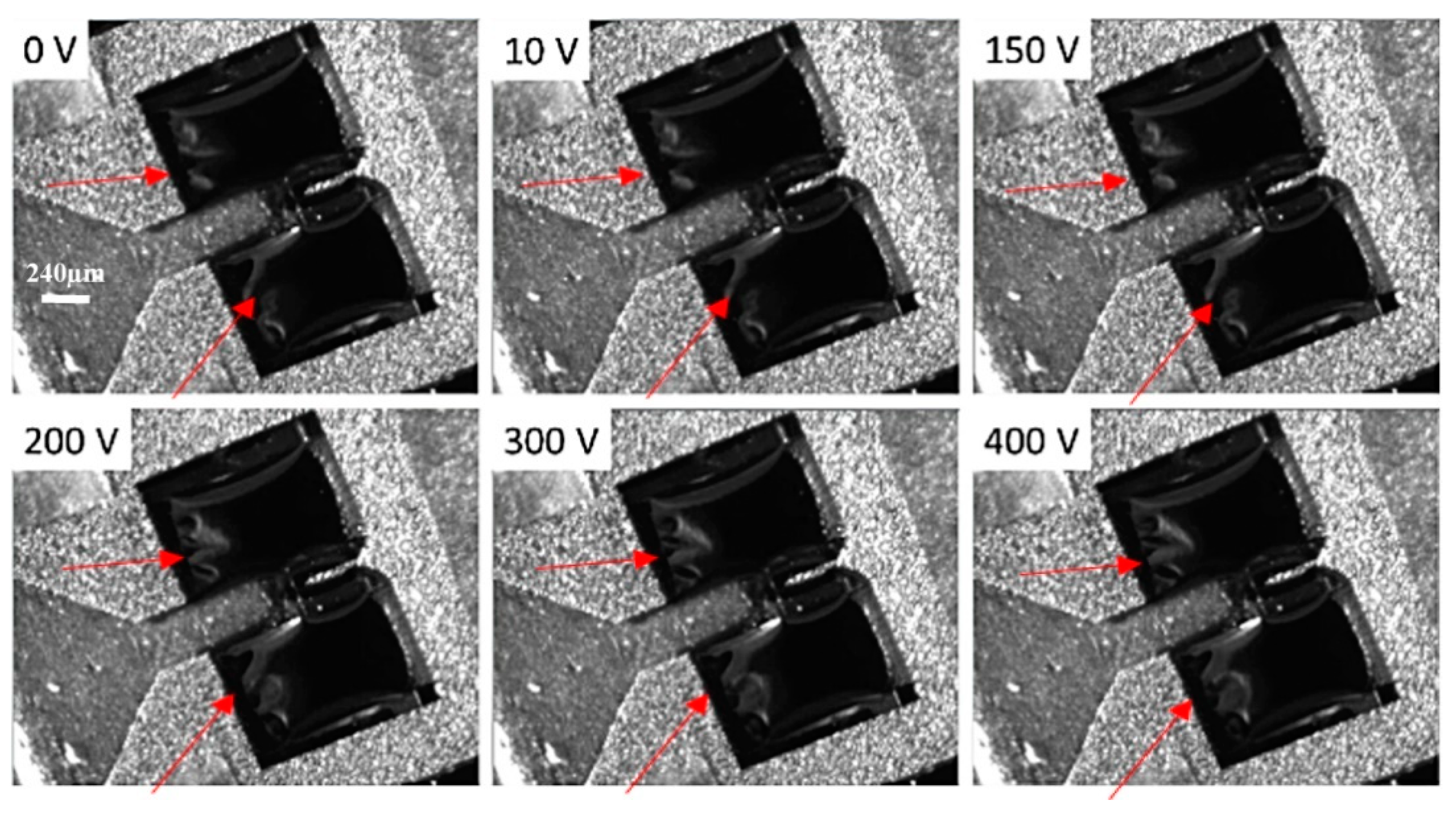
Although the simulation shows promising line resolution and FOV, there were challenges found in fabrication and in tests performed of the resonating design. The main obstacle is apparently on overcoming the weight of the proof mass at the tip of the cantilever. It was found later that SU-8 cantilever is much softer than the model based on the published material properties. Several design changes were made including the proof mass thickness and the no-resonating design to further simplify the fabrication and operation.
For the non-resonating scanner design, the same parametric study to optimize the design was also performed using Architect3D in CoventorWare. The modified actuator shown in
Figure 7 is used to increase the in-plane electrostatic force, leading to a larger FOV. When the device is in operation, Electrode 1 and 3 are applied with the same waveform function of
Vosinωt and Electrode 2 and 4 are applied with a
Vocosωt, where
ω is the resonant frequency of the high-frequency mode and
Vo is the amplitude of the input voltage. For low frequency direction, all electrodes were driven by a same wave function with lower frequency. Suppose the waveguide is simultaneously driven at the above two frequencies, a raster scanning motion will appear at the distal end.
The result of the deflection angles of the optimized scanner is shown in
Figure 8. The simulation shows that when the device is operating at 10 Hz in the non-resonant frequency direction (vertical direction) and 1.343 kHz in the resonant frequency direction (horizontal direction), the FOV are 16 and 15 mrad, respectively and a 130-line resolution at 0.08 Rayleigh damping and ±20 V input.
The reduction in the proof mass from 300 µm × 300 µm × 24 µm in resonating design to 60 µm × 60 µm × 4 µm in non-resonating design was needed to simplify the fabrication and also to prevent the cantilever from bending too much due to the additional weight (Figure 19a). The width of the waveguide was also reduced from 55 to 20 µm to increase vibration in the horizontal direction.
In the parametric study, the geometry of the waveguide (the cross section and the length) dominated the line resolution of the scanner; the resolution increased with a flatter and shorter waveguide. The rib waveguide had a very similar resonant frequency response as long as the dimensions of the width of the ridge section were kept relatively small compared to the width of the slab section (<4×). All other geometric parameters did not appear to affect the line resolution significantly. In the analyses for the actuator and arm geometries, larger actuator pads allowed larger actuation; however, the sizes of the pads are limited by the design footprint (3 mm × 3 mm) defined for the previous endoscopic application. The largest angle of rotation achieved by the investigated push–pull designs was ~0.44 and 0.089 rad in vertical and horizontal direction respectively (for the resonating design) and 71 and 15 mrad, for the non-resonating design A shorter rotating arm appears to provide a larger angle of rotation. These findings suggest that the waveguide and the actuator layout can be considered separately to optimize the line resolution and scanning magnitude as we have shown in the analysis.
2.3. Optical Analysis
To optimize the light transmission and coupling between the tip of the input fiber and the cantilever beam requires modal analysis and investigation of the system’s coupling efficiency. The waveguide for the scanner has a rib waveguide feature (
Figure 9), and it is made of an epoxy-based SU-8 negative-tone photoresist. The wavelength range required for the proposed display application is 400 to 650 nm. The final dimension of the waveguide structure was slightly different from the mechanical simulation. The slab was reduced to 20 microns and the proof mass also reduced to 60 μm × 60 μm × 4 μm to simplify the fabrication and improve dynamic performance of the cantilever vibration. One way to predict the dimensions of the rib waveguide structure was based on the single mode conditions proposed by Soref [
26].
where
q is defined as:
where
for transverse electric (TE) modes and
and
for TM modes.
It can be seen from equation 4 that for single mode operation. Therefore, H ≥ 0.314 µm at λ = 400 nm and H ≥ 0.531 µm at λ = 650 nm.
To maintain a single mode operation based on the above condition in TE polarization for any given
H, the rib width
W must be designed and operated less than or equal to the value on the curve (
Figure 10). By fixing the ratio (
r) between the overall height (
H) and the slab height (
h) to 0.5, we generate a list of waveguide dimensions that we can use for the scanner design (
Figure 6 and
Table 2. In case 1, the cross section of the rib waveguide has dimensions relative to the core diameter of a single mode fiber (2.9 to 3.9 µm mode field diameter for 400 to 600 nm wavelengths), which is an ideal geometry for the proposed end-butted coupling design. Assuming the same input applies at the center of the rib waveguide, the output power for different waveguide geometries is summarized in
Table 2.
Using modal analysis, based on a SU-8 (n = 1.578 at λ = 650 nm and n = 1.624 at λ = 400 nm [
27]) rib waveguide structure with a rib width (
W): waveguide height (
H): slab height (
h) ratio as shown in
Table 2, the result confirms single mode operation for TE mode input with wavelengths between 400 to 650 nm.
Figure 11 shows the index and modal profile of all three cases observed at 1.282 mm from the coupling end at λ = 650 nm (
Figure 11b–d). The profile is similar at 400 nm (
Figure 11a). Fields all appear confined and single mode.
An optical simulation using Rsoft beam propagation program (BMP) software was performed to analyze the coupling efficiency. In order to simplify the analysis, scattering and absorption were neglected and it is assumed that the input to the waveguide is a single mode Gaussian beam. The numerical simulation is based on a SU-8 rib waveguide structure with a rib width: waveguide height: slab height ratio of 4:4:2. The results confirmed single mode operation for TE mode input with wavelengths between 400 and 650 nm. As shown in
Figure 12, a very low light loss for wavelengths operates between 0.4 and 0.65 µm if center of the input mode field aligns with the center core of the waveguide (X = 0, Y = 2). For an input with a Gaussian profile, the coupling efficiency for both wavelengths was around 96.5% and 97% for λ = 400 nm and λ = 0.65 μm, respectively. Minimum light attenuation was observed along the taper and cantilever waveguide sections. The light throughput is roughly the same as the initial coupling efficiency (93.8% and 94.2% respectively). The same coupling efficiency and throughput was also observed if the input was a zeroth order mode. However, the alignment of the input with respect to the core of the rib waveguide greatly affects the coupling efficiency.
Table 2 summarizes the output power as a function of input position operating at 650 nm wavelength. When fiber is vertical lateral displacement (y direction), the coupling loss was less significant than the horizontal displacement (x direction) as long as the beam was confined inside the waveguide. This is most likely the main contribution to the observed low coupling efficiency in the measurement. It is also shown in our previous multimode 100 µm × 85 µm × 2100 µm SU-8 rectangular waveguide that combine loss stem from mode coupling, scattering and absorption is around 28.6% [
17,
18]. The simulation also shows that the shape of the proof mass does not matter in the optical simulation, because as long as the input beam is confined inside the ridge area of the waveguide, single mode propagation is maintained. As shown in
Figure 12a,b, both output fields at 400 and 650 nm appear to be single mode and nicely confined inside the waveguide. The far field intensity profile is also generated and match quite closely to the experiment result with ~ 0.22° in x direction and 8.8° in y direction FWHM at λ = 400 and 650 nm (
Figure 8). As expected, the FWHM for 400 nm is slightly smaller than 650 nm.


