
Omnidirectional and Broadband Antireflection Effect with Tapered Silicon Nanostructures Fabricated with Low-Cost and Large-Area Capable Nanosphere Lithography


Abstract
:1. Introduction
2. Experimental Section
3. Result and Discussion
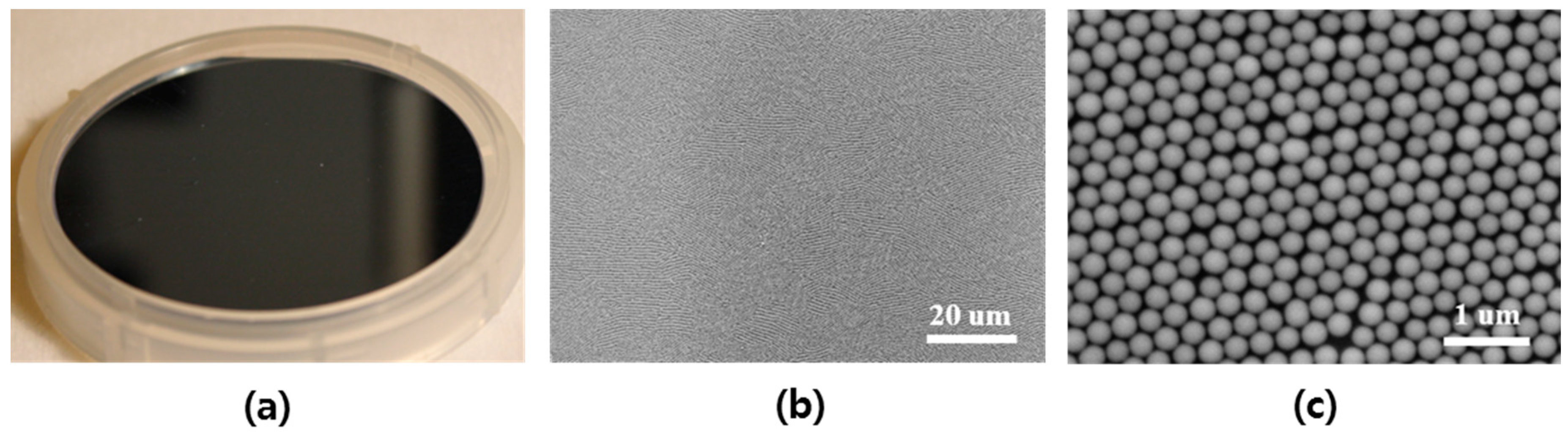
3.1. Spin-Coating of 2-Dimensional SNSs
3.2. Nanostructure Fabrication with RIE Process
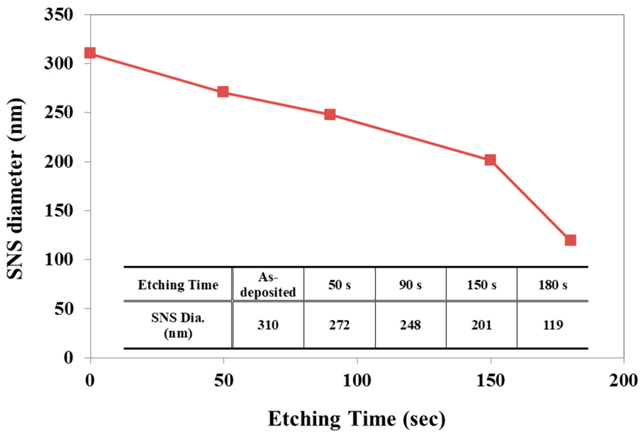
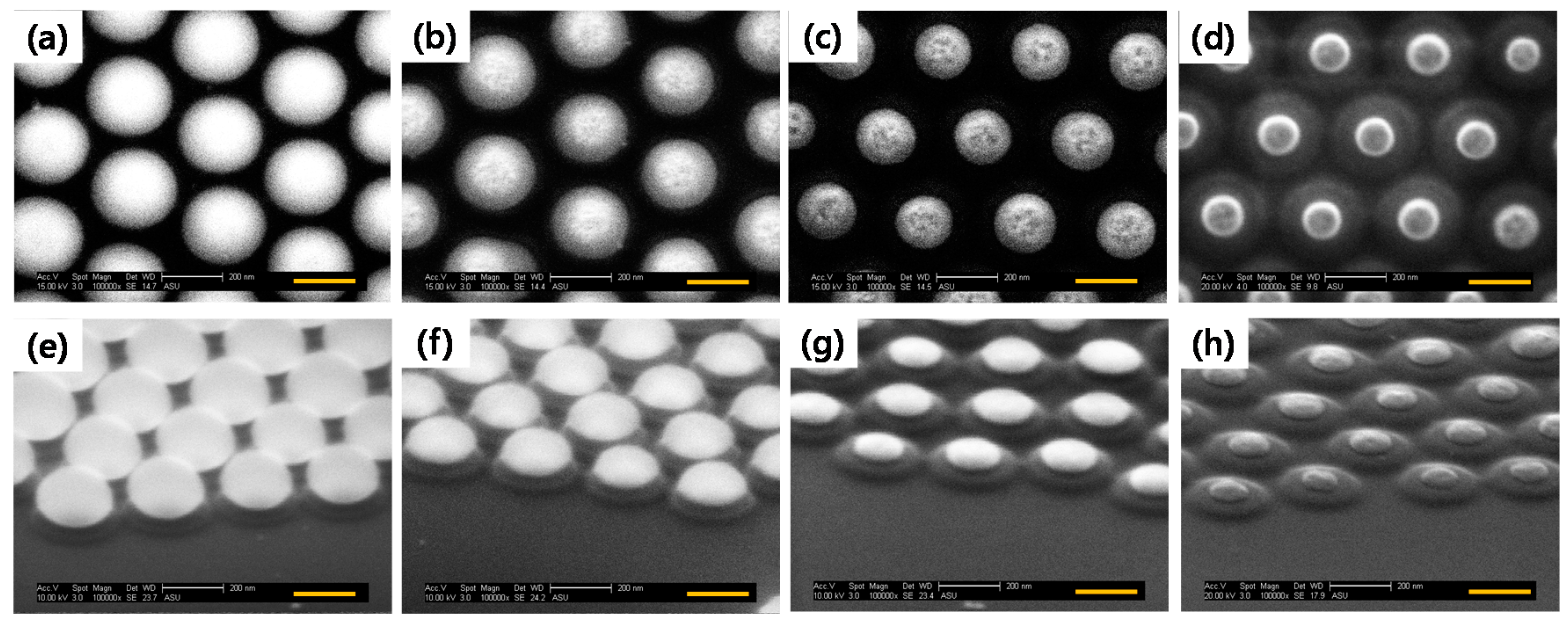
3.2.1. SNS Size Reduction with CHF3/Ar Gases RIE
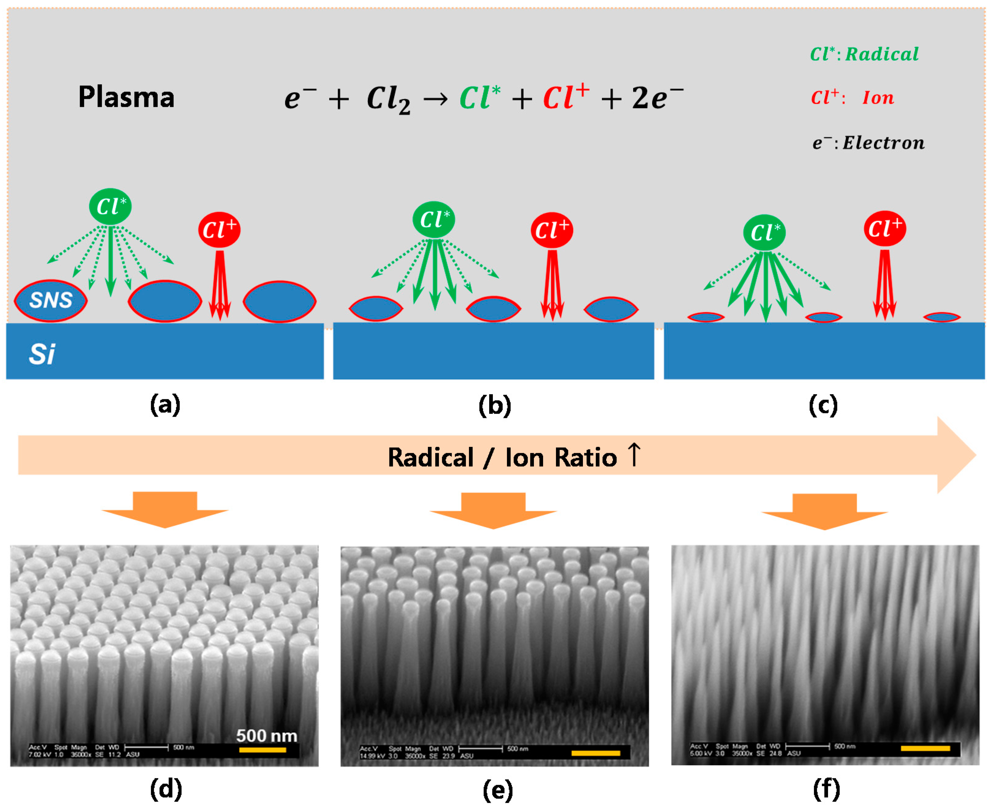
3.2.2. Si Vertical Etching with Cl2 Gas RIE
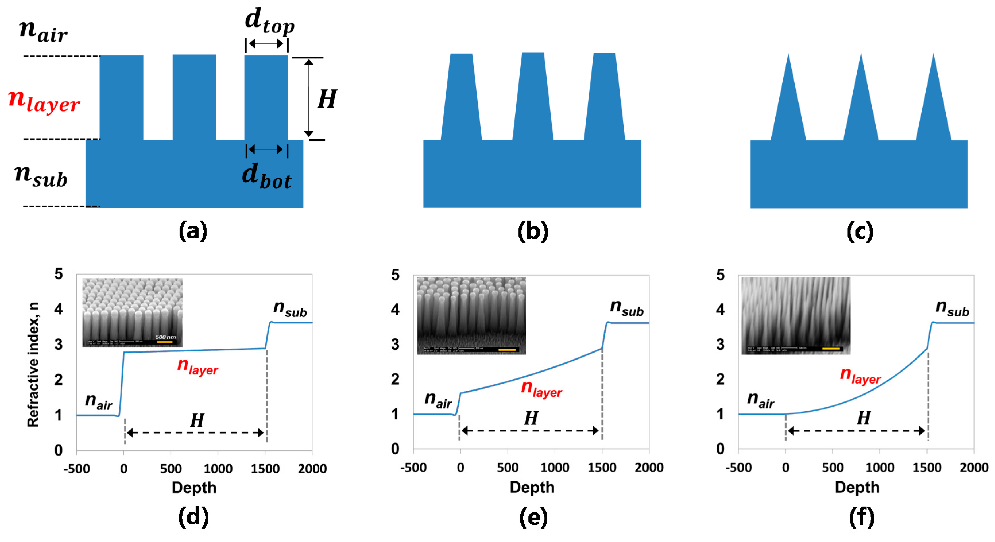
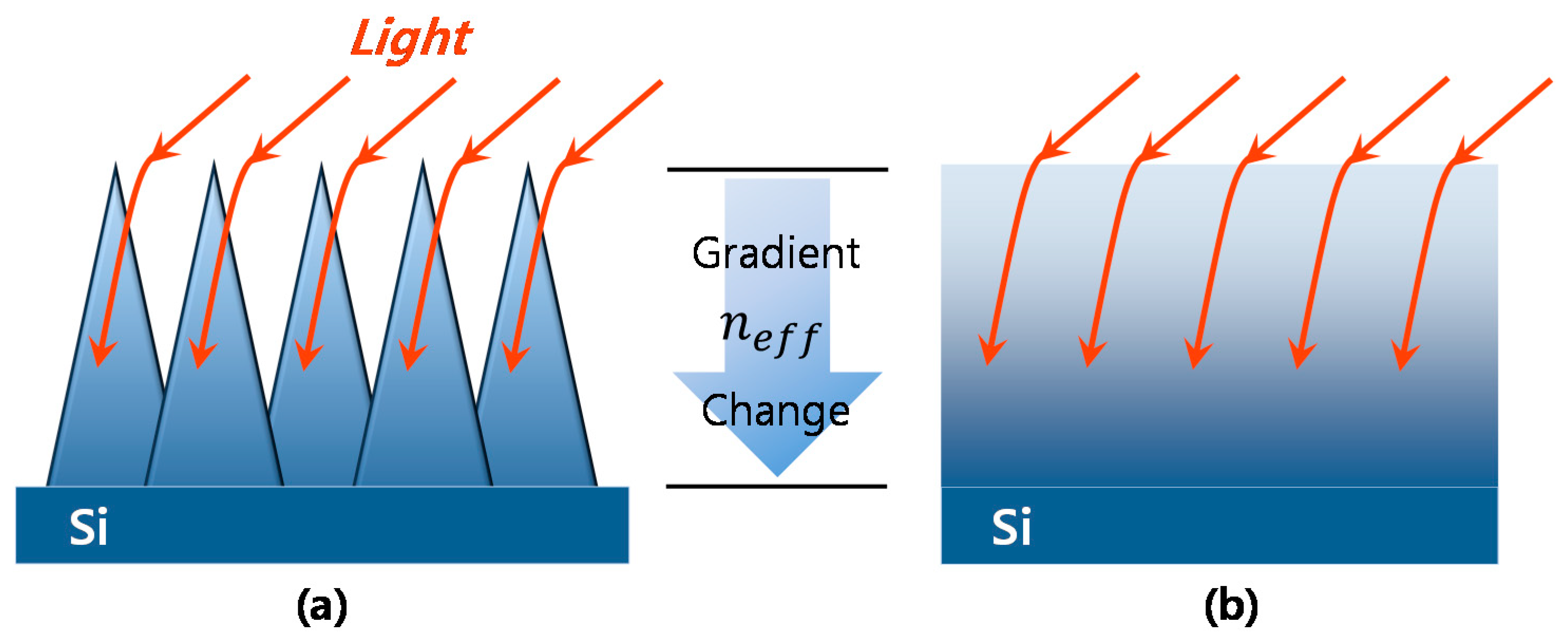
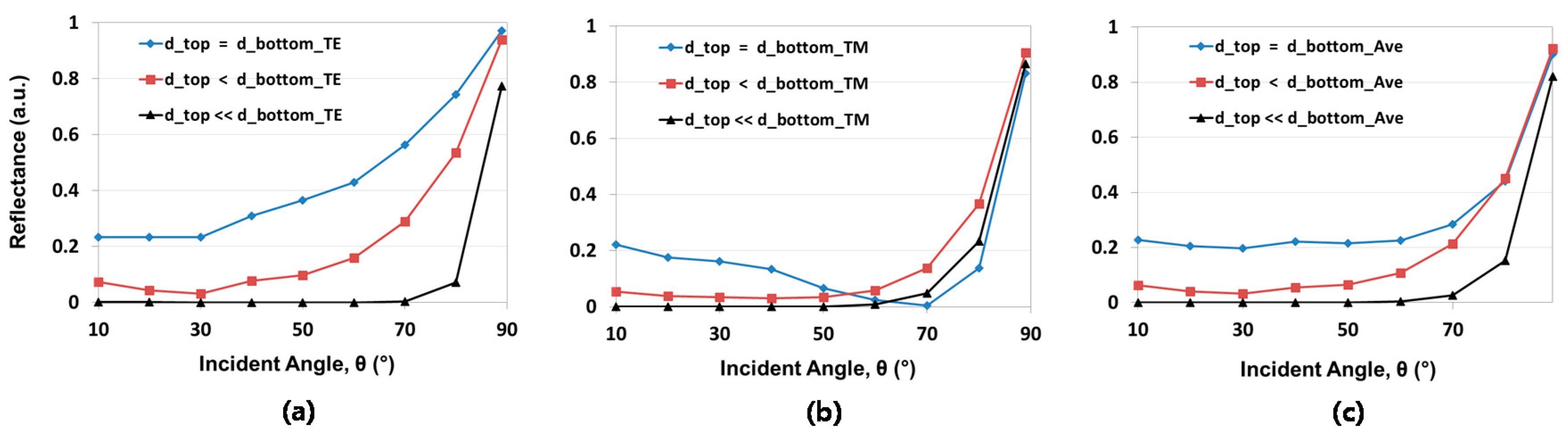
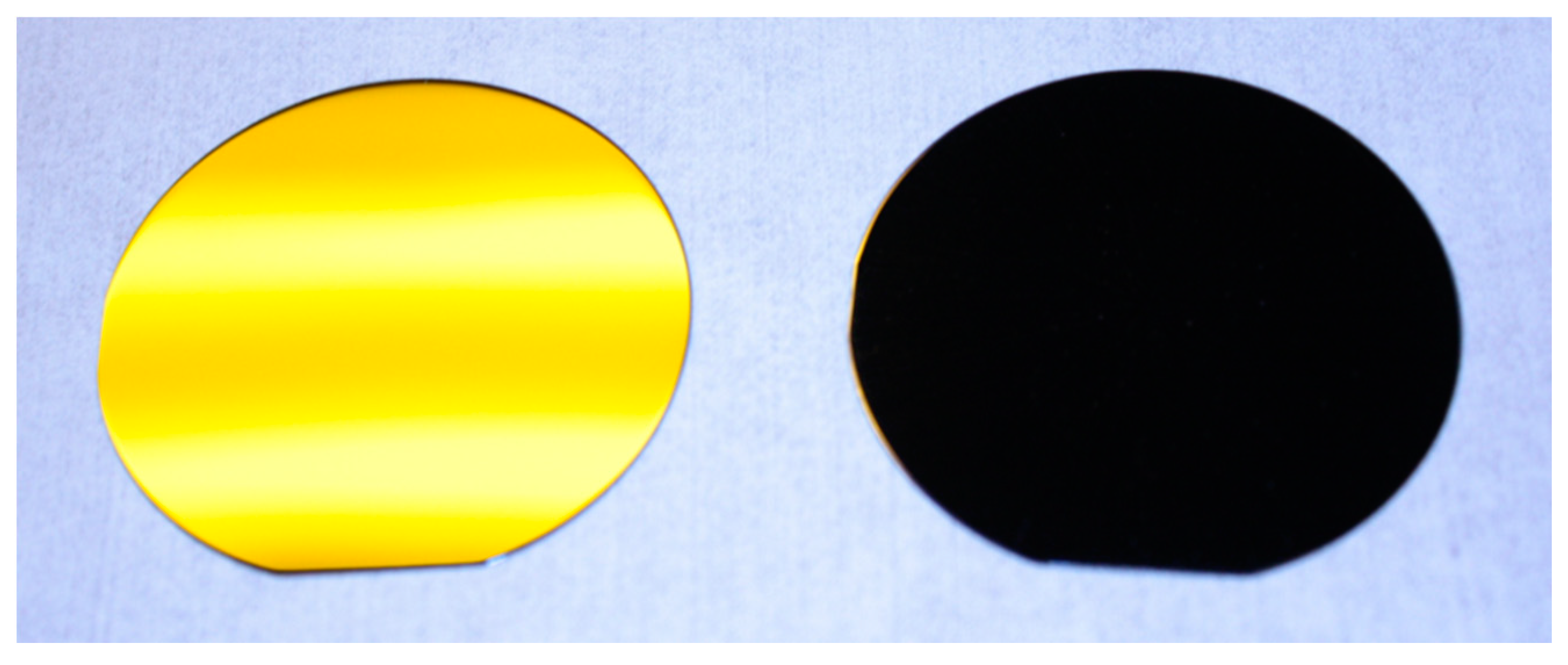
3.2.3. Optical Properties of Fabricated Si Nanostructures
4. Conclusions
Supplementary Materials
Author Contributions
Funding
Conflicts of Interest
References
- Peng, K.Q.; Xu, Y.; Wu, Y.; Yan, Y.; Lee, S.; Zhu, J. Aligned single-crystalline Si nanowire arrays for photovoltaic applications. Small 2005, 1, 1062–1067. [Google Scholar] [CrossRef] [PubMed]
- Muskens, O.L.; Rivas, J.G.; Algra, R.E.; Bakkers, E.P.A.M.; Lagendijk, A. Design of light scattering in nanowire materials for photovoltaic applications. Nano Lett. 2008, 8, 2638–2642. [Google Scholar] [CrossRef] [PubMed]
- Garnett, E.C.; Yang, P. Silicon nanowire radial p-n junction solar cells. J. Am. Chem. Soc. 2008, 130, 9224–9225. [Google Scholar] [CrossRef] [PubMed]
- Sivakov, V.; Andrä, G.; Gawlik, A.; Berger, A.; Plentz, J.; Falk, F.; Christiansen, S.H. Silicon Nanowire-Based Solar Cells on Glass: Synthesis, Optical Properties, and Cell Parameters. Nano Lett. 2009, 9, 1549–1554. [Google Scholar] [CrossRef] [PubMed]
- Zhu, J.; Yu, Z.; Burkhard, G.F.; Hsu, C.M.; Connor, S.T.; Xu, Y.; Wang, Q.; McGehee, M.; Fan, S.; Cui, Y. Optical Absorption Enhancement in Amorphous Silicon Nanowire and Nanocone Arrays. Nano Lett. 2009, 9, 279–282. [Google Scholar] [CrossRef] [Green Version]
- Garnett, E.; Yang, P. Light trapping in silicon nanowire solar cells. Nano Lett. 2010, 10, 1082–1087. [Google Scholar] [CrossRef]
- Huang, Y.-F.; Chattopadhyay, S.; Jen, Y.-J.; Peng, C.-Y.; Liu, T.-A.; Hsu, Y.-K.; Pan, C.-L.; Lo, H.-C.; Hsu, C.-H.; Chang, Y.-H.; et al. Improved broadband and quasi-omnidirectional anti-reflection properties with biomimetic silicon nanostructures. Nat. Nanotechnol. 2007, 2, 770–774. [Google Scholar] [CrossRef]
- Yang, J.; Luo, F.; Kao, T.S.; Li, X.; Ho, G.W.; Teng, J.; Luo, X.; Hong, M. Design and fabrication of broadband ultralow reflectivity black Si surfaces by laser micro/nanoprocessing. Light Sci. Appl. 2014, 3, e185. [Google Scholar] [CrossRef]
- Aiken, D.J. High performance anti-reflection coatings for broadband multi-junction solar cells. Sol. Energy Mater. Sol. Cells 2000, 64, 393–404. [Google Scholar] [CrossRef] [Green Version]
- Sankur, H.; Southwell, W.H. Broad-band gradient-index antireflection coating for znse. Appl. Opt. 1984, 23, 2770–2773. [Google Scholar] [CrossRef]
- Dobrowolski, J.A.; Poitras, D.; Ma, P.; Vakil, H.; Acree, M. Toward perfect antireflection coatings: Numerical investigation. Appl. Opt. 2002, 41, 3075–3083. [Google Scholar] [CrossRef] [PubMed]
- Koynov, S.; Brandt, M.S.; Stutzmann, M. Black nonreflecting silicon surfaces for solar cells. Appl. Phys. Lett. 2006, 88. [Google Scholar] [CrossRef]
- Chutinan, A.; John, S. Light trapping and absorption optimization in certain thin-film photonic crystal architectures. Phys. Rev. A 2008, 78, 023825. [Google Scholar] [CrossRef] [Green Version]
- Tobias, I.; Luque, A.; Marti, A. Light intensity enhancement by diffracting structures in solar cells. J. Appl. Phys. 2008, 104, 034502. [Google Scholar] [CrossRef] [Green Version]
- Lin, C.; Povinelli, M.L. Optical absorption enhancement in silicon nanowire arrays with a large lattice constant for photovoltaic applications. Opt. Express 2009, 17, 19371–19381. [Google Scholar] [PubMed]
- Han, S.E.; Chen, G. Toward the lambertian limit of light trapping in thin nanostructured silicon solar cells. Nano Lett. 2010, 10, 4692–4696. [Google Scholar] [CrossRef]
- Huang, Z.; Gao, K.; Wang, X.; Xu, C.; Song, X.; Shi, L.; Zhang, Y.; Hoex, B.; Shen, W. Large-area MACE Si nano-inverted-pyramids for PERC solar cell application. Sol. Energy 2019, 188, 300–304. [Google Scholar]
- Lee, Y.; Woo, Y.; Lee, D.-K.; Kim, I. Fabrication of quasi-hexagonal Si nanostructures and its application for flexible crystalline ultrathin Si solar cells. Sol. Energy 2020, 208, 957–965. [Google Scholar]
- Juhasz, R.; Elfstrom, N.; Linnros, J. Controlled fabrication of silicon nanowires by electron beam lithography and electrochemical size reduction. Nano Lett. 2005, 5, 275–280. [Google Scholar] [CrossRef]
- Zhang, J.; Shokouhi, B.; Cui, B. Tilted nanostructure fabrication by electron beam lithography. J. Vac. Sci. Technol. B 2012, 30, 06F302. [Google Scholar] [CrossRef]
- Ertorer, E.; Vasefi, F.; Keshwah, J.; Najiminaini, M.; Halfpap, C.; Langbein, U.; Carson, J.J.L.; Hamilton, D.W.; Mittler, S. Large area periodic, systematically changing, multishape nanostructures by laser interference lithography and cell response to these topographies. J. Biomed. Opt. 2013, 18. [Google Scholar] [CrossRef] [PubMed] [Green Version]
- Tan, C.; Peng, C.S.; Pakarinen, J.; Pessa, M.; Petryakov, V.N.; Verevkin, Y.K.; Zhang, J.; Wang, Z.; Olaizola, S.M.; Berthou, T.; et al. Ordered nanostructures written directly by laser interference. Nanotechnology 2009, 20. [Google Scholar] [CrossRef] [PubMed]
- Rasband, W. Imagej; U.S. National Institutes of Health: Bethesda, MD, USA, 1997–2018; Available online: https://imagej.nih.gov/ij/ (accessed on 7 December 2020).
- Ogi, T.; Modesto-Lopez, L.B.; Iskandar, F.; Okuyama, K. Fabrication of a large area monolayer of silica particles on a sapphire substrate by a spin coating method. Colloids Surf. Physicochem. Eng. Asp. 2007, 297, 71–78. [Google Scholar] [CrossRef]
- Zhang, L.; Qiao, S.; Jin, Y.; Chen, Z.; Gu, H.; Lu, G.Q. Magnetic hollow spheres of periodic mesoporous organosilica and Fe3O4 nanocrystals: Fabrication and structure control. Adv. Mater. 2008, 20, 805–809. [Google Scholar] [CrossRef]
- Izak-Nau, E.; Voetz, M.; Eiden, S.; Duschl, A.; Puntes, V.F. Altered characteristics of silica nanoparticles in bovine and human serum: The importance of nanomaterial characterization prior to its toxicological evaluation. Part. Fibre Toxicol. 2013, 10. [Google Scholar] [CrossRef] [Green Version]
- Wan, Q.; Ramsey, C.; Baran, G. Thermal pretreatment of silica composite filler materials. J. Therm. Anal. Calorim. 2010, 99, 237–243. [Google Scholar] [CrossRef] [Green Version]
- Schneider, C.A.; Rasband, W.S.; Eliceiri, K.W. NIH Image to ImageJ: 25 years of image analysis. Nat. Methods 2012, 9, 671–675. [Google Scholar] [CrossRef]
- Hsu, C.-M.; Connor, S.T.; Tang, M.X.; Cui, Y. Wafer-scale silicon nanopillars and nanocones by Langmuir-Blodgett assembly and etching. Appl. Phys. Lett. 2008, 93, 133109. [Google Scholar] [CrossRef]
- Huang, J.X.; Kim, F.; Tao, A.R.; Connor, S.; Yang, P.D. Spontaneous formation of nanoparticle stripe patterns through dewetting. Nat. Mater. 2005, 4, 896–900. [Google Scholar] [CrossRef]
- Hulteen, J.C.; Vanduyne, R.P. Nanosphere lithography-A materials general fabrication process for periodic particle array surfaces. J. Vac. Sci. Technol. A Vac. Surf. Film. 1995, 13, 1553–1558. [Google Scholar] [CrossRef]
- Mihi, A.; Ocana, M.; Miguez, H. Oriented colloidal-crystal thin films by spin-coating microspheres dispersed in volatile media. Adv. Mater. 2006, 18, 2244–2249. [Google Scholar] [CrossRef] [Green Version]
- Choi, J.-Y.; Alford, T.; Honsberg, C.B. Solvent-controlled spin-coating method for large-scale area deposition of two-dimensional silica nanosphere assembled layers. Langmuir 2014, 30, 5732–5738. [Google Scholar] [CrossRef] [PubMed]
- Choi, J.-Y.; Alford, T.; Honsberg, C.B. Fabrication of periodic silicon nanopillars in a two-dimensional hexagonal array with enhanced control on structural dimension and period. Langmuir 2015, 31, 4018–4023. [Google Scholar] [CrossRef] [PubMed]
- Jansen, H.; Gardeniers, H.; de Boer, M.; Elwenspoek, M.; Fluitman, J. A survey on the reactive ion etching of silicon in microtechnology. J. Micromechanics Microengineering 1996, 6, 14. [Google Scholar] [CrossRef] [Green Version]
- Lai, S.; Johnson, D.; Westerman, R. Aspect ratio dependent etching lag reduction in deep silicon etch processes. J. Vac. Sci. Technol. A Vac. Surf. Film. 2006, 24, 1283–1288. [Google Scholar] [CrossRef] [Green Version]
- Li, Y.; Zhang, J.; Zhu, S.; Dong, H.; Jia, F.; Wang, Z.; Sun, Z.; Zhang, L.; Li, Y.; Li, H. Biomimetic surfaces for high-performance optics. Adv. Mater. 2009, 21, 4731–4734. [Google Scholar] [CrossRef]
- Stavenga, D.; Foletti, S.; Palasantzas, G.; Arikawa, K. Light on the moth-eye corneal nipple array of butterflies. Proc. R. Soc. B Biol. Sci. 2005, 273, 661–667. [Google Scholar] [CrossRef] [Green Version]
- Sahouane, N.; Necaibia, A.; Ziane, A.; Dabou, R.; Bouraiou, A.; Mostefaoui, M.; Rouabhia, A. Realization and modeling of multilayer antireflection coatings for solar cells application. Mater. Res. Express 2018, 5, 065515. [Google Scholar] [CrossRef]
- Schubert, M.F.; Mont, F.W.; Chhajed, S.; Poxson, D.J.; Kim, J.K.; Schubert, E.F. Design of multilayer antireflection coatings made from co-sputtered and low-refractive-index materials by genetic algorithm. Opt. Express 2008, 16, 5290–5298. [Google Scholar] [CrossRef] [Green Version]
- Sai, H.; Fujii, H.; Arafune, K.; Ohshita, Y.; Yamaguchi, M.; Kanamori, Y.; Yugami, H. Antireflective subwavelength structures on crystalline Si fabricated using directly formed anodic porous alumina masks. Appl. Phys. Lett. 2006, 88, 201116. [Google Scholar] [CrossRef]
- Poitras, D.; Dobrowolski, J.A. Toward perfect antireflection coatings 2 Theory. Appl. Opt. 2004, 43, 1286–1295. [Google Scholar] [CrossRef] [PubMed]
- Huang, Y.F.; Chattopadhyay, S. Nanostructure surface design for broadband and angle-independent antireflection. J. Nanophotonics 2013, 7, 073594. [Google Scholar] [CrossRef]


| Solvent | Water | DMF | |
|---|---|---|---|
| Properties | |||
| Vapor Pressure (Torr, at 20 °C) | 17.54 | 2.70 | |
| Viscosity (cP) | 1.0 | 0.92 | |
| Wetting Angle () |  |  | |
| Initial SNS Dia. | 272 | 201 | 119 |
|---|---|---|---|
| SEM Images |  |  |  |
| Top dia. | 263 12 | 162 16 | <20 |
| Bottom dia. | 281 7 | 276 8 | 269 23 |
| Height | 1425 22 | 1488 27 | 1612 38 |
Publisher’s Note: MDPI stays neutral with regard to jurisdictional claims in published maps and institutional affiliations. |
© 2021 by the authors. Licensee MDPI, Basel, Switzerland. This article is an open access article distributed under the terms and conditions of the Creative Commons Attribution (CC BY) license (http://creativecommons.org/licenses/by/4.0/).
Share and Cite
Kim, S.; Jeong, G.S.; Park, N.Y.; Choi, J.-Y. Omnidirectional and Broadband Antireflection Effect with Tapered Silicon Nanostructures Fabricated with Low-Cost and Large-Area Capable Nanosphere Lithography. Micromachines 2021, 12, 119. https://doi.org/10.3390/mi12020119
Kim S, Jeong GS, Park NY, Choi J-Y. Omnidirectional and Broadband Antireflection Effect with Tapered Silicon Nanostructures Fabricated with Low-Cost and Large-Area Capable Nanosphere Lithography. Micromachines. 2021; 12(2):119. https://doi.org/10.3390/mi12020119
Chicago/Turabian StyleKim, Sangho, Gwan Seung Jeong, Na Yeon Park, and Jea-Young Choi. 2021. "Omnidirectional and Broadband Antireflection Effect with Tapered Silicon Nanostructures Fabricated with Low-Cost and Large-Area Capable Nanosphere Lithography" Micromachines 12, no. 2: 119. https://doi.org/10.3390/mi12020119
APA StyleKim, S., Jeong, G. S., Park, N. Y., & Choi, J.-Y. (2021). Omnidirectional and Broadband Antireflection Effect with Tapered Silicon Nanostructures Fabricated with Low-Cost and Large-Area Capable Nanosphere Lithography. Micromachines, 12(2), 119. https://doi.org/10.3390/mi12020119