Area-Scalable 109-Cycle-High-Endurance FeFET of Strontium Bismuth Tantalate Using a Dummy-Gate Process


Abstract
:1. Introduction
2. Materials and Methods
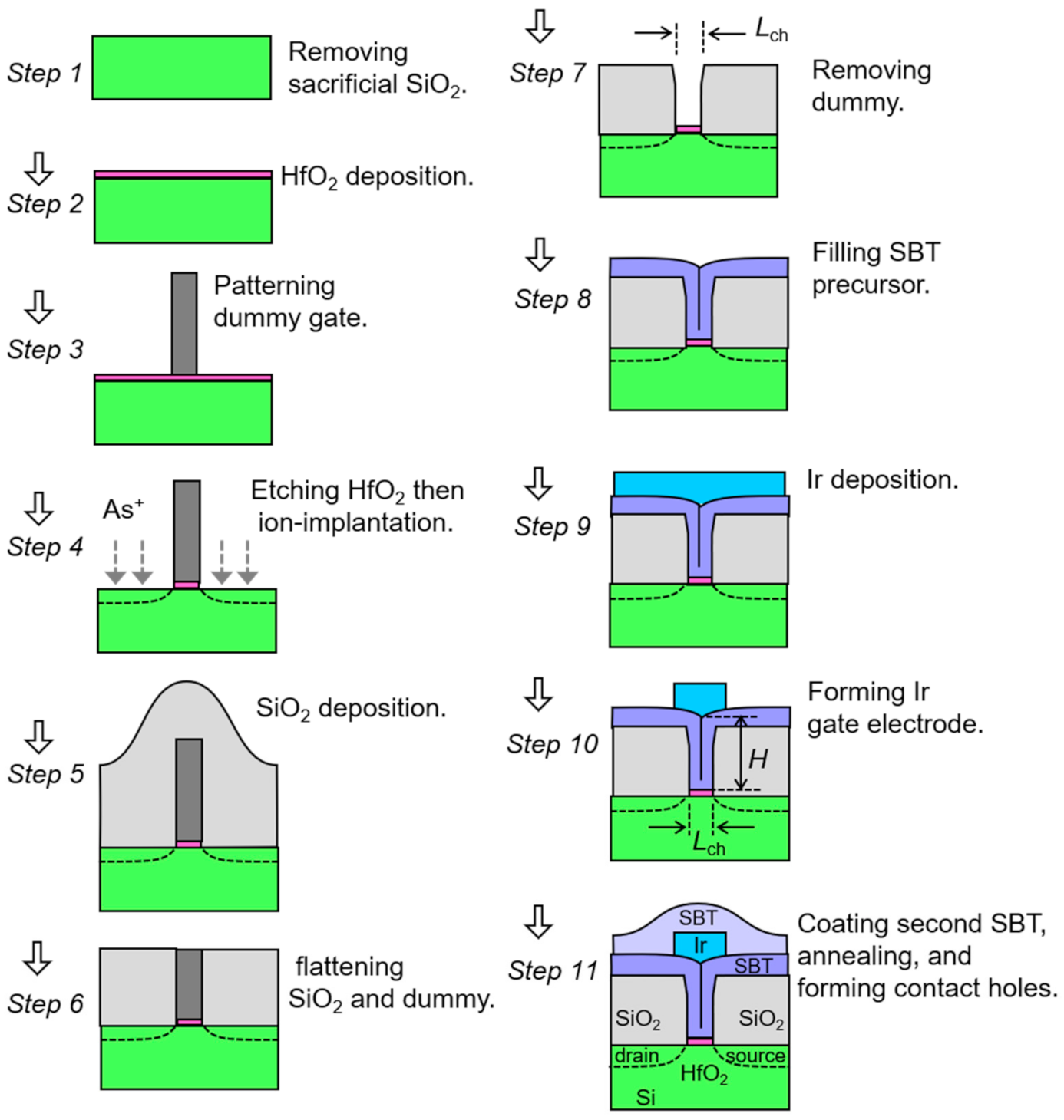
2.1. Device Fabrication Process
- Step 1: Si substrate preparation.A p-type Si substrate patterned with FET active areas was prepared. Local-oxidation-of-silicon (LOCOS) process was used in the patterning for device isolation. The LOCOS patterns with various channel widths (W) were designed in a sample chip. Areas for source-, drain- and substrate-contact holes on the Si were heavily ion-doped. Sacrificial SiO2 on Si was removed with buffered hydrogen fluoride.
- Step 2: Insulator deposition.
- Step 3: Lithography.Electron-beam (EB) lithography was performed by spin-coating an organic resist, exposing 130 kV EB, and developing. Resist patterns 550 nm tall were left on the HfO2/Si. They were later used as ion-implantation mask in Step 4 and as dummy gates in Step 7.
- Step 4: Ion implantation.HfO2 uncovered with resist was etched out by inductively-coupled-plasma reactive-ion etching (ICP-RIE). On the exposed Si, As+ ions were implanted for source and drain. The energy and dose conditions were 4 keV and 5.0 × 10¹²/cm2.
- Step 5: SiO2 deposition.An 830 nm thick SiO2 was deposited to cover the resist patterns on the substrate by 300 W rf sputtering in 0.1 Pa Ar.
- Step 6: Flattening SiO2.The SiO2 was etched back and flattened by ICP-RIE with 1.0 Pa Ar-CF4 mixed gas until tops of the resists or dummy gates were exposed.
- Step 7: Leaving grooves on gates.The dummy-gate substances were selectively removed by O2 plasma ashing. There remained grooves in a 410 nm tall SiO2 isolation. The grooves were located on the HfO2 with self-aligned source and drain regions prepared in Step 4. The whole chip was rapidly annealed at 800 °C in ambient N2.
- Step 8: Ferroelectric deposition.SBT precursor film was deposited to fill up the grooves by a metal-organic-chemical-vapor deposition (MOCVD) system (WACOM R&D, Nihonbashi, Tokyo, Japan). Sources of Bi(C5H11O2)3, Sr[Ta(OC2H5)5(OC2H4OCH3)]2 and Ta(OCH2CH3)5 (Tri Chemical Laboratories Inc., Uenohara, Yamanashi, Japan) were used [6]. As-deposited precursor-film thickness was estimated as 80 nm on a flat place of the substrate.
- Step 9: Metal deposition.Ir was deposited by rf sputtering on the SBT precursor layer. Resist mask was patterned for gate electrodes by EB lithography.
- Step 10: Forming gate electrodes.Ir uncovered with resist was etched out by Ar+ ion milling. Then, the resist mask was removed by O2 plasma ashing.
- Step 11: FeFET completed.SBT precursor was deposited again by MOCVD to cover the substrate [6]. The whole substrate was annealed for crystallization of the SBT to show ferroelectricity. The annealing condition was at 780 °C in an O2-N2 mixed gas we investigated before [8]. Finally, contact holes for gate, source, drain and substrate were formed by ultraviolet g-line lithography and Ar+ ion milling.
2.2. Reason for Using SBT in FeFET
3. Results and Discussion
3.1. Device Dimensions
3.2. Electrical Characterizations
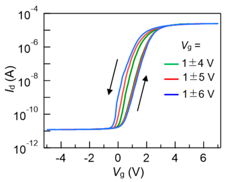
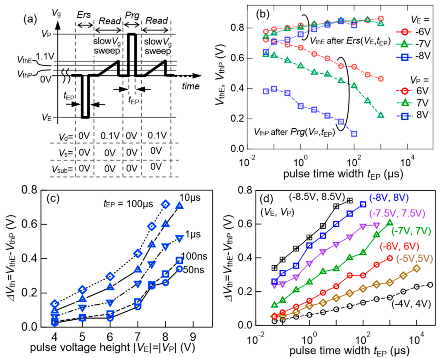
3.2.1. Memory Windows
3.2.2. Retention
3.2.3. Endurance
4. Summary
Author Contributions
Funding
Institutional Review Board Statement
Informed Consent Statement
Data Availability Statement
Acknowledgments
Conflicts of Interest
References
- Sakai, S.; Ilangovan, R. Metal-ferroelectric-insulator-semiconductor memory FET with long retention and high endurance. IEEE Electron Device Lett. 2004, 25, 369–371. [Google Scholar] [CrossRef]
- Yan, K.; Takahashi, M.; Sakai, S. Electrical properties of ferroelectric-gate FETs with SrBi2Ta2O9 formed using MOCVD technique. Appl. Phys. A Mater. Sci. Process. 2012, 108, 835–842. [Google Scholar] [CrossRef]
- Sakai, S.; Zhang, W.; Takahashi, M. Dynamic analog characteristics of 109 cycle-endurance low-voltage nonvolatile ferroelectric-gate memory transistors. In Proceedings of the 2017 IEEE 9th International Memory Workshop, Monterey, CA, USA, 14–17 May 2017; pp. 95–98. [Google Scholar] [CrossRef]
- Hai, L.V.; Takahashi, M.; Sakai, S. Fabrication and characterization of sub-0.6-μm ferroelectric-gate field-effect transistors. Semicond. Sci. Technol. 2010, 25, 115013. [Google Scholar] [CrossRef]
- Zhang, W.; Takahashi, M.; Sakai, S. Electrical properties of CaxSr1-xBi2Ta2O9 ferroelectric-gate field-effect transistors. Semicond. Sci. Technol. 2013, 28, 085003. [Google Scholar] [CrossRef]
- Hai, L.V.; Takahashi, M.; Zhang, W.; Sakai, S. Novel process for widening memory window of sub-200nm ferroelectric-gate field-effect transistor by ferroelectric coating the gate-stack sidewall. Semicond. Sci. Technol. 2015, 30, 015024. [Google Scholar] [CrossRef]
- Hai, L.V.; Takahashi, M.; Zhang, W.; Sakai, S. 100-nm-size ferroelectric-gate field-effect transistor with 108-cycle endurance. Jpn. J. Appl. Phys. 2015, 54, 088004. [Google Scholar] [CrossRef]
- Zhang, W.; Takahashi, M.; Sasaki, Y.; Kusuhara, M.; Sakai, S. 3.3 V write-voltage Ir/Ca0.2Sr0.8Bi2Ta2O9/HfO2/Si ferroelectric-gate field-effect transistors with 109 endurance and good retention. Jpn. J. Appl. Phys. 2017, 56, 04CE04. [Google Scholar] [CrossRef]
- Sakai, S.; Takahashi, M.; Takeuchi, K.; Li, Q.-H.; Horiuchi, T.; Wang, S.; Yun, K.-Y.; Takamiya, M.; Sakurai, T. Highly scalable Fe(ferroelectric)-NAND cell with MFIS(metal-ferroelectric-insulator-semiconductor) structure for sub-10nm tera-bit capacity NAND flash memories. In Proceedings of the 2008 Joint Non-Volatile Semiconductor Memory Workshop and International Conference on Memory Technology and Design, Opio, France, 18–22 May 2008; pp. 103–105. [Google Scholar] [CrossRef]
- Zhang, X.; Miyaji, K.; Takahashi, M.; Takeuchi, K.; Sakai, S. 0.5V bit-line-voltage self-boost-programming in ferroelectric-NAND flash memory. In Proceedings of the 2011 3rd IEEE International Memory Workshop, Monterey, CA, USA, 22–25 May 2011; pp. 155–158. [Google Scholar] [CrossRef]
- Zhang, X.; Takahashi, M.; Takeuchi, K.; Sakai, S. 64 kbit ferroelectric-gate-transistor-integrated NAND flash memory with 7.5 V program and long data retention. Jpn. J. Appl. Phys. 2012, 51, 04DD01. [Google Scholar] [CrossRef]
- Takahashi, M.; Zhang, W.; Sakai, S. High-endurance ferroelectric NOR flash memory using (Ca,Sr)Bi2Ta2O9 FeFETs. In Proceedings of the 2018 IEEE 10th International Memory Workshop, Kyoto, Japan, 13–16 May 2018; pp. 58–61. [Google Scholar] [CrossRef]
- De Araujo, C.A.P.; Cuchiaro, J.D.; McMillan, L.D.; Scott, M.C.; Scott, J.F. Fatigue-free ferroelectric capacitors with platinum electrodes. Nature 1995, 374, 627–629. [Google Scholar] [CrossRef]
- Noguchi, T.; Hase, T.; Miyasaka, Y. Analysis of the dependence of ferroelectric properties of strontium bismuth tantalate (SBT) thin film on the composition and process temperature. Jpn. J. Appl. Phys. 1996, 35, 4900–4904. [Google Scholar] [CrossRef]
- Lettieri, J.; Jia, Y.; Urbanik, M.; Weber, C.I.; Maria, J.-P.; Schlom, D.G.; Li, H.; Ramesh, R.; Uecker, R.; Reiche, P. Epitaxial growth of (001)-oriented and (110)-oriented SrBi2Ta2O9 thin films. Appl. Phys. Lett. 1995, 66, 221–223. [Google Scholar] [CrossRef]
- Ishikawa, K.; Funakubo, H. Electrical properties of (001)- and (116)-oriented epitaxial SrBi2Ta2O9 thin films prepared by metalorganic chemical vapor deposition. Appl. Phys. Lett. 1999, 75, 1970–1972. [Google Scholar] [CrossRef]
- Ishikawa, K.; Funakubo, H.; Saito, K.; Suzuki, T.; Nishi, Y.; Fujimoto, M. Crystal structure and electrical properties of epitaxial SrBi2Ta2O9 films. J. Appl. Phys. 2000, 87, 8018–8023. [Google Scholar] [CrossRef]
- Lee, H.N.; Visinoiu, A.; Senz, S.; Harnagea, C.; Pignolet, A.; Hesse, D.; Gösele, U. Structural and electrical anisotropy of (001)-, (116)-, and (103)-oriented epitaxial SrBi2Ta2O9 thin films on SrTiO3 substrates grown by pulsed laser deposition. J. Appl. Phys. 2000, 88, 6658–6664. [Google Scholar] [CrossRef]
- Amanuma, K.; Hase, T.; Miyasaka, Y. Preparation and ferroelectric properties of SrBi2Ta2O9 thin films. Appl. Phys. Lett. 1995, 66, 221–223. [Google Scholar] [CrossRef]
- Atsuki, T.; Soyama, N.; Yonezawa, T.; Ogi, K. Preparation of Bi-based ferroelectric thin films by Sol-Gel method. Jpn. J. Appl. Phys. 1995, 34, 5096–5099. [Google Scholar] [CrossRef]
- Robertson, J.; Chen, C.W.; Warren, W.L.; Gutleben, C.D. Electronic structure of the ferroelectric layered perovskite SrBi2Ta2O9. Appl. Phys. Lett. 1996, 69, 1704–1706. [Google Scholar] [CrossRef]
- Harnagea, C.; Pignolet, A.; Alexe, M.; Hesse, D.; Gösele, U. Quantitative ferroelectric characterization of single submicron grains in Bi-layered perovskite thin films. Appl. Phys. A 2000, 70, 261–267. [Google Scholar] [CrossRef]
- Kalinin, S.V.; Gruverman, A.; Bonnell, D.A. Quantitative analysis of nanoscale switching in SrBi2Ta2O9 thin films by piezoresponse force microscopy. Appl. Phys. Lett. 2004, 85, 795. [Google Scholar] [CrossRef]
- Amorín, H.; Shvartsman, V.V.; Kholkin, A.L.; Costa, M.E.V. Ferroelectric and dielectric anisotropy in high-quality SrBi2Ta2O9 single crystals. Appl. Phys. Lett. 2004, 85, 5667. [Google Scholar] [CrossRef]
- Yu, T.; Shen, Z.X.; Toh, W.S.; Xue, J.M.; Wang, J. Size effect on the ferroelectric phase transition in SrBi2Ta2O9 nanoparticles. J. Appl. Phys. 2003, 94, 618–620. [Google Scholar] [CrossRef]
- Gruverman, A. Scaling effect on statistical behavior of switching parameters of ferroelectric capacitors. Appl. Phys. Lett. 1999, 75, 1452–1454. [Google Scholar] [CrossRef]
- Tamura, T.; Arimoto, Y.; Ishiwara, H. A New Circuit Simulation Model of Ferroelectric Capacitors. Jpn. J. Appl. Phys. 2002, 41, 2654–2657. [Google Scholar] [CrossRef]
- Pan, B.; Yu, H.; Wu, D.; Zhou, X.H.; Liu, J.-M. Dynamic response and hysteresis dispersion scaling of ferroelectric SrBi2Ta2O9 thin films. Appl. Phys. Lett. 2003, 83, 1406–1408. [Google Scholar] [CrossRef]
- Lee, W.-J.; Cho, C.-R.; Kim, S.-H.; You, I.-K.; Kim, B.W.; Yu, B.-G.; Shin, C.H.; Lee, H.C. Etching Behavior and Damage Recovery of SrBi2Ta2O9 Thin Films. Jpn. J. Appl. Phys. 1999, 38, L1428–L1431. [Google Scholar] [CrossRef]
- Asami, K.; Koiwa, I.; Yamanobe, T. Effects of Ion Etching and Annealing in O2 Atmosphere Following Ion Etching on Properties and Chemistry of Sr0.9Bi2.1Ta2O9+α Thin Films. Jpn. J. Appl. Phys. 1999, 38, 5423–5427. [Google Scholar] [CrossRef]
- Stafford, L.; Margot, J.; Delprat, S.; Chaker, M.; Pearton, S.J. Influence of redeposition on the plasma etching dynamics. J. Appl. Phys. 2007, 101, 083303. [Google Scholar] [CrossRef]
- Efremov, A.M.; Kim, D.-P.; Kim, C.-I. Investigation of thin films etching mechanisms in plasma. J. Vsc. Sci. Technol. A 2003, 21, 1017–1023. [Google Scholar] [CrossRef]
- Shimakawa, Y.; Kubo, Y.; Nakagawa, Y.; Goto, S.; Kamiyama, T.; Asano, H.; Izumi, F. Crystal structure and ferroelectric properties of ABi2Ta2O9 (A = Ca, Sr, and Ba). Phys. Rev. B 2000, 61, 6559–6564. [Google Scholar] [CrossRef]
- Noguchi, Y.; Shimizu, H.; Miyayama, M.; Oikawa, K.; Kamiyama, T. Ferroelectric properties and structure distortion in A-site-modified SrBi2Ta2O9. Jpn. J. Appl. Phys. 2001, 40, 5812–5815. [Google Scholar] [CrossRef]
- Das, R.R.; Bhattacharya, P.; Pe´rez, W.; Katiyar, R.S. Ferroelectric properties of laser-ablated Sr1-xAxBi2Ta2O9 thin films (where A = Ba, Ca). Appl. Phys. Lett. 2002, 80, 637–639. [Google Scholar] [CrossRef]
- Das, R.R.; Bhattacharya, P.; Pe´rez, W.; Katiyar, R.S. Influence of Ca on structural and ferroelectric properties of laser ablated SrBi2Ta2O9 thin films. Jpn. J. Appl. Phys. 2003, 42, 162–165. [Google Scholar] [CrossRef]
- Development of the 1T FeRAM: Towards the Realization of the Ultra-Gbit Next-Generation Semiconductor Memory. AIST Research Results Archive, 24 October 2002. Available online: https://www.aist.go.jp/aist_e/list/latest_research/2002/20021024/20021024.html (accessed on 14 December 2020).
- Sakai, S.; Takahashi, M.; Ilangovan, R. Long-retention ferroelectric-gate FET with a (HfO2)x(Al2O3)1-x buffer-insulating layer for 1T FeRAM. In Proceedings of the 2004 IEDM Technical Digest. IEEE International Electron Devices Meeting, San Francisco, CA, USA, 13–15 December 2004; pp. 915–918. [Google Scholar] [CrossRef]
- Sakai, S.; Ilangovan, R.; Takahashi, M. Pt/SrBi2Ta2O9/Hf-Al-O/Si field-effect-transistor with long retention using unsaturated ferroelectric polarization switching. Jpn. J. Appl. Phys. 2004, 43, 7876–7878. [Google Scholar] [CrossRef]
- Li, Q.H.; Sakai, S. Characterization of Pt/SrBi2Ta2O9/Hf-Al-O/Si field-effect transistors at elevated temperatures. Appl. Phys. Lett. 2006, 89, 222910. [Google Scholar] [CrossRef]
- Li, Q.H.; Takahashi, M.; Horiuchi, T.; Wang, S.Y.; Sakai, S. Threshold-voltage distribution of Pt/SrBi2Ta2O9/Hf-Al-O/Si MFIS FETs. Semicond. Sci. Technol. 2008, 23, 045011. [Google Scholar] [CrossRef]
- Li, Q.H.; Horiuchi, T.; Wang, S.Y.; Takahashi, M.; Sakai, S. Threshold voltage adjustment of ferroelectric-gate field effect transistors by ion implantation. Semicond. Sci. Technol. 2009, 24, 025012. [Google Scholar] [CrossRef]
- Sakai, S.; Zhang, W.; Takahashi, M. Method for disclosing invisible physical properties in metal-ferroelectric-insulator-semiconductor gate stacks. J. Phys. D Appl. Phys. 2017, 50, 165107. [Google Scholar] [CrossRef]
- Zhang, W.; Takahashi, M.; Sakai, S. Investigation of ferroelectric grain sizes and orientations in Pt/CaxSr1–xBi2Ta2O9/Hf–Al–O/Si high performance ferroelectric-gate field-effect-transistors. Materials 2019, 12, 399. [Google Scholar] [CrossRef] [Green Version]
- Takahashi, M.; Sakai, S. Self-aligned-gate metal/ferroelectric/insulator/semiconductor field-effect transistors with long memory retention. Jpn. J. Appl. Phys. 2005, 44, L800–L802. [Google Scholar] [CrossRef]
- Horiuchi, T.; Takahashi, M.; Li, Q.H.; Wang, S.Y.; Sakai, S. Lowered operation voltage in Pt/SBi2Ta2O9/HfO2/Si ferroelectric-gate field-effect transistors by oxynitriding Si. Semicond. Sci. Technol. 2010, 25, 055005. [Google Scholar] [CrossRef]
- Takahashi, M.; Horiuchi, T.; Li, Q.H.; Wang, S.Y.; Sakai, S. Basic operation of novel ferroelectric CMOS circuits. Electron. Lett. 2008, 44, 467–468. [Google Scholar] [CrossRef]
- Takahashi, M.; Wang, S.Y.; Horiuchi, T.; Sakai, S. FeCMOS logic inverter circuits with nonvolatile-memory function. IEICE Electron. Express 2009, 6, 831–836. [Google Scholar] [CrossRef] [Green Version]
- Wang, S.Y.; Takahashi, M.; Li, Q.H.; Takeuchi, K.; Sakai, S. Operational method of a ferroelectric (Fe)-NAND flash memory array. Semicond. Sci. Technol. 2009, 24, 105029. [Google Scholar] [CrossRef]
- Miyaji, K.; Noda, S.; Hatanaka, T.; Takahashi, M.; Sakai, S.; Takeuchi, K. A 1.0 V power supply, 9.5 GByte/sec write speed, Single-Cell Self-Boost program scheme for Ferroelectric NAND Flash SSD. In Proceedings of the 2010 IEEE International Memory Workshop, Seoul, South Korea, 16–19 May 2010; pp. 1–4. [Google Scholar] [CrossRef]
- Zhang, X.; Takahashi, M.; Sakai, S. FeFET logic circuits for operating a 64 kb FeNAND flash memory array. Integr. Ferroelectr. 2012, 132, 114–121. [Google Scholar] [CrossRef]
- Sakai, S.; Zhang, X.Z.; Hai, L.V.; Zhang, W.; Takahashi, M. Downsizing and memory array integration of Pt/SrBi2Ta2O9/Hf-Al-O/Si ferroelectric-gate field-effect transistors. In Proceedings of the 2012 12th Annual Non-Volatile Memory Technology Symposium, Singapore, 31 October–2 November 2012; pp. 55–59. [Google Scholar] [CrossRef]
- Sakai, S.; Takahashi, M.; Motohashi, K.; Yamaguchi, Y.; Yui, N.; Kobayashi, T. Large-area pulsed-laser deposition of dielectric and ferroelectric thin films. J. Vac. Sci. Technol. A 2007, 25, 903–907. [Google Scholar] [CrossRef]
- Sakai, S. Semiconductor-Ferroelectric Storage Devices and Processes for Producing The Same. U.S. Patent 7,226,795, 2007. [Google Scholar]
- Böscke, T.S.; Müller, J.; Bräuhaus, D.; Schröder, U.; Böttger, U. Ferroelectricity in hafnium oxide: CMOS compatible ferroelectric field effect transistors. In Proceedings of the 2011 IEDM Technical Digest. IEEE International Electron Devices Meeting, Washington, DC, USA, 5–7 December 2011; pp. 24.5.1–24.5.4. [Google Scholar] [CrossRef]
- Müller, J.; Yurchuk, E.; Schlösser, T.; Paul, J.; Hoffmann, R.; Müller, S.; Martin, D.; Slesazeck, S.; Polakowski, P.; Sundqvist, J.; et al. Ferroelectricity in HfO2 enables nonvolatile data storage in 28 nm HKMG. In Proceedings of the 2012 Symposium on VLSI Technology, Honolulu, HI, USA, 12–14 June 2012; pp. 25–26. [Google Scholar] [CrossRef]
- Ali, T.; Polakowski, P.; Riedel, S.; Büttner, T.; Kämpfe, T.; Rudolph, M.; Pätzold, B.; Seidel, K.; Löhr, D.; Hoffmann, R.; et al. Silicon doped hafnium oxide (HSO) and hafnium zirconium oxide (HZO) based FeFET: A material relation to device physics. Appl. Phys. Lett. 2018, 112, 222903. [Google Scholar] [CrossRef]
- Fukuda, M.; Mizubayashi, W.; Kohno, A.; Miyazaki, S.; Hirose, M. Analysis of Tunnel Current through Ultrathin Gate Oxides. Jpn. J. Appl. Phys. 1998, 37, L1534–L1536. [Google Scholar] [CrossRef]
- Shrenk, A.; Heiser, G. Modeling and simulation of tunneling through ultra-thin gate dielectrics. J. Appl. Phys. 1997, 81, 7900–7908. [Google Scholar] [CrossRef] [Green Version]
- Takahashi, M.; Sakai, S. 2.3.3 Requirements to the F Layer, Chap.2 Development of high-endurance and long-retention FeFETs of Pt/CaySr1−yBi2Ta2O9/(HfO2)x(Al2O3)1−x/Si gate stacks. In Ferroelectric-Gate Field Effect Transistor Memories, 2nd ed.; Park, B.-E., Ishiwara, H., Okuyama, M., Sakai, S., Yoon, S.-M., Eds.; Springer: Singapore, Singapore, 2020; pp. 35–37. [Google Scholar] [CrossRef]
- Kingston, R.; Neustadter, S.F. Calculation of the Space Charge, Electric Field, and Free Carrier Concentration at the Surface of a Semiconductor. J. Appl. Phys. 1955, 26, 718–720. [Google Scholar] [CrossRef]
- Sze, S.M. Chap.7, MIS Diode and Charge-Coupled Device. In Physics of Semiconductor Devices, 2nd ed.; John Wiley & Sons: New York, NY, USA, 1981; pp. 366–369. [Google Scholar]
- Zhang, F.; Hsu, S.T.; Ono, Y.; Ulrich, B.; Zhuang, W.; Ying, H.; Stecker, L.; Evans, D.R.; Maa, J. Fabrication and characterization of sub-micron metal-ferroelectric-insulator-semiconductor field effect transistors with Pt/Pb5Ge3O11/ZrO2/Si structure. Jpn. J. Appl. Phys. 2001, 40, L635–L637. [Google Scholar] [CrossRef]
- Li, T.; Hsu, S.T.; Ulrich, B.; Ying, H.; Stecker, L.; Evans, D.; Ono, Y.; Maa, J.; Lee, J.J. Fabrication and characterization of a Pb5Ge3O11 one-transistor-memory device. Appl. Phys. Lett. 2001, 79, 1661–1663. [Google Scholar] [CrossRef]
- Müller, J.; Böscke, T.S.; Schröder, U.; Mueller, S.; Bräuhaus, D.; Böttger, U.; Frey, L.; Mikolajick, T. Ferroelectricity in simple binary ZrO2 and HfO2. Nano Lett. 2012, 12, 4318–4323. [Google Scholar] [CrossRef]
- Shimizu, T.; Katayama, K.; Kiguchi, T.; Akama, A.; Konno, T.J.; Sakata, O.; Funakubo, H. The demonstration of significant ferroelectricity in epitaxial Y-doped HfO2 film. Sci. Rep. 2016, 6, 32931. [Google Scholar] [CrossRef] [PubMed] [Green Version]
- Yurchuk, E.; Müller, J.; Hoffmann, R.; Paul, J.; Martin, D.; Boschke, R.; Schlösser, T.; Müller, S.; Slesazeck, S.; Bentum, R.; et al. HfO2-Based Ferroelectric Field-Effect Transistors with 260 nm Channel Length and Long Data Retention. In Proceedings of the 2012 IEEE International Memory Workshop, Milan, Italy, 20–23 May 2012; pp. 1–4. [Google Scholar] [CrossRef]
- Trentzsch, M.; Flachowsky, S.; Richter, R.; Paul, J.; Reimer, B.; Utess, D.; Jansen, S.; Mulaosmanovic, H.; Müller, S.; Slesazeck, S.; et al. A 28nm HKMG super low power embedded NVM technology based on ferroelectric FETs. In Proceedings of the 2016 IEEE International Electron Devices Meeting, San Francisco, CA, USA, 3–7 December 2016; pp. 11.5.1–11.5.4. [Google Scholar] [CrossRef]
- Mulaosmanovic, H.; Breyer, E.T.; Mikolajick, T.; Slesazeck, S. Ferroelectric FETs with 20-nm-Thick HfO2 Layer for Large Memory Window and High Performance. IEEE Trans. Electron. Devices 2019, 66, 3828–3833. [Google Scholar] [CrossRef]
- Zhou, H.; Ocker, J.; Mennenga, M.; Noack, M.; Müller, S.; Trentzsch, M.; Dünkel, S.; Beyer, S.; Mikolajick, T. Endurance and targeted programming behavior of HfO2-FeFETs. In Proceedings of the 2020 IEEE International Memory Workshop, Dresden, Germany, 17–20 May 2020; pp. 1–4. [Google Scholar] [CrossRef]
- Wong, H.; Iwai, H. On the scaling issues and high-κ replacement of ultrathin gate dielectrics for nanoscale MOS transistors. Microelectron. Eng. 2006, 83, 1867–1904. [Google Scholar] [CrossRef]
- Tagantsev, A.K.; Stolichnov, I.; Setter, N.; Cross, J.S.; Tsukada, M. Non-Kolmogorov-Avrami switching kinetics in ferroelectric thin films. Phys. Rev. B 2002, 66, 214109. [Google Scholar] [CrossRef]
- Jo, J.Y.; Yang, S.M.; Kim, T.H.; Lee, H.N.; Yoon, J.-G.; Park, S.; Jo, Y.; Jung, M.H.; Noh, T.W. Nonlinear dynamics of domain-wall propagation in epitaxial ferroelectric thin films. Phys. Rev. Lett. 2009, 102, 045701. [Google Scholar] [CrossRef] [Green Version]


Publisher’s Note: MDPI stays neutral with regard to jurisdictional claims in published maps and institutional affiliations. |
© 2021 by the authors. Licensee MDPI, Basel, Switzerland. This article is an open access article distributed under the terms and conditions of the Creative Commons Attribution (CC BY) license (http://creativecommons.org/licenses/by/4.0/).
Share and Cite
Takahashi, M.; Sakai, S. Area-Scalable 109-Cycle-High-Endurance FeFET of Strontium Bismuth Tantalate Using a Dummy-Gate Process. Nanomaterials 2021, 11, 101. https://doi.org/10.3390/nano11010101
Takahashi M, Sakai S. Area-Scalable 109-Cycle-High-Endurance FeFET of Strontium Bismuth Tantalate Using a Dummy-Gate Process. Nanomaterials. 2021; 11(1):101. https://doi.org/10.3390/nano11010101
Chicago/Turabian StyleTakahashi, Mitsue, and Shigeki Sakai. 2021. "Area-Scalable 109-Cycle-High-Endurance FeFET of Strontium Bismuth Tantalate Using a Dummy-Gate Process" Nanomaterials 11, no. 1: 101. https://doi.org/10.3390/nano11010101
APA StyleTakahashi, M., & Sakai, S. (2021). Area-Scalable 109-Cycle-High-Endurance FeFET of Strontium Bismuth Tantalate Using a Dummy-Gate Process. Nanomaterials, 11(1), 101. https://doi.org/10.3390/nano11010101