
Recent Progress on ZnO Nanowires Cold Cathode and Its Applications


Abstract
:1. Introduction
2. Synthesis
2.1. Chemical Vapor Deposition
2.2. Hydrothermal Method
2.3. Thermal Oxidation
3. Field Emission
3.1. Field-Emission Properties
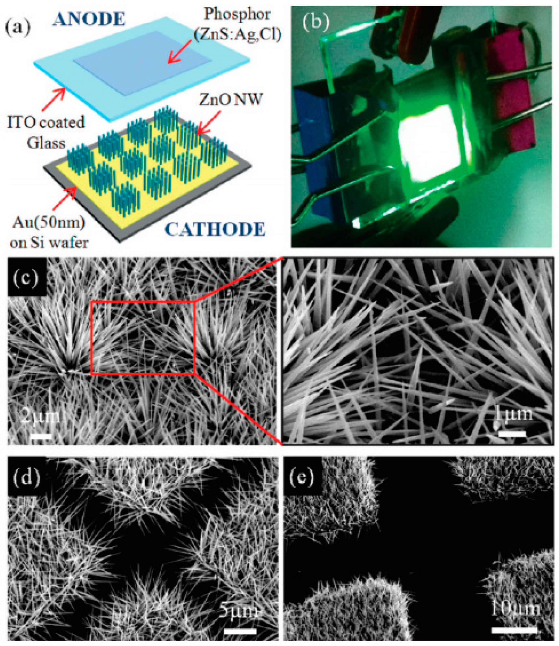
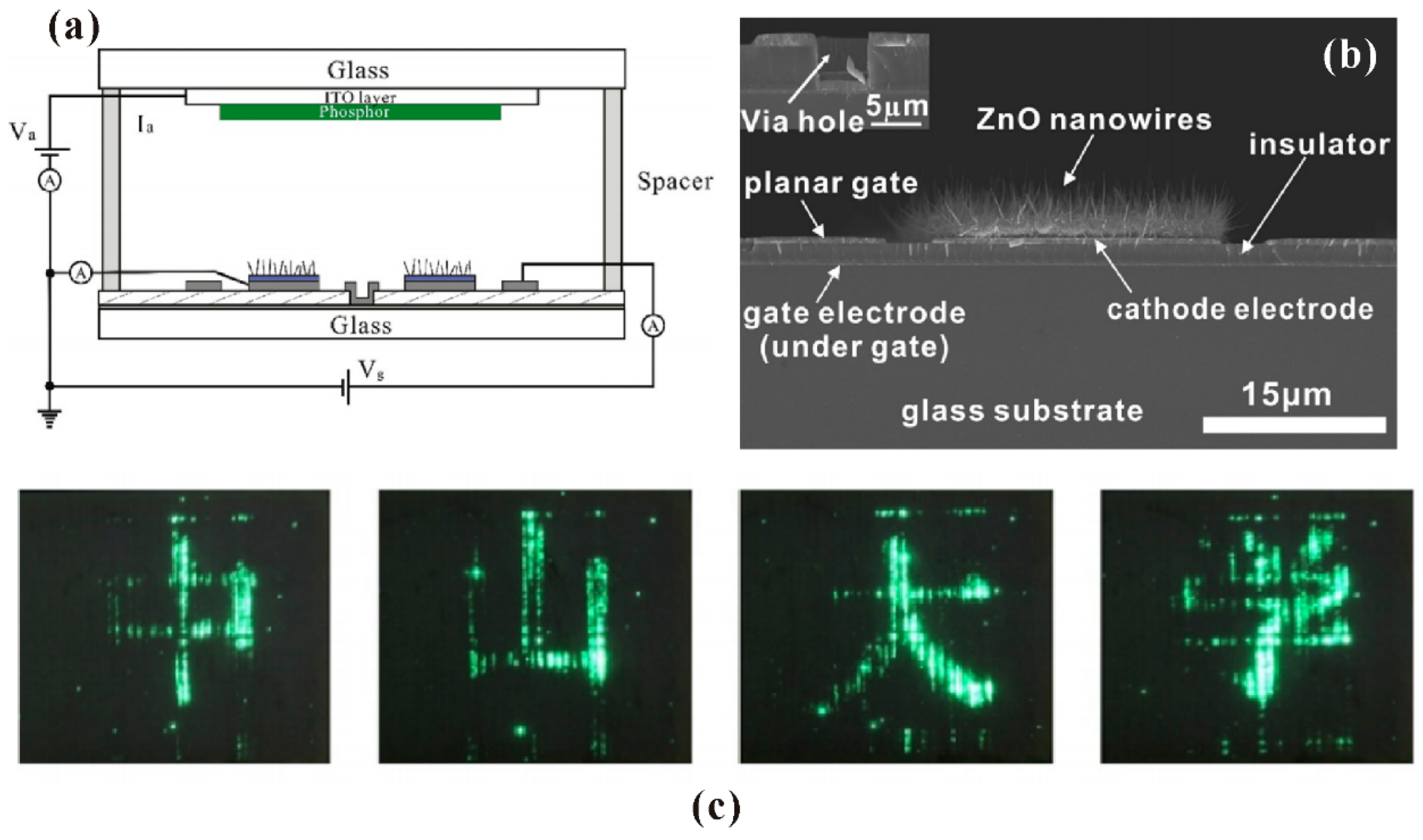
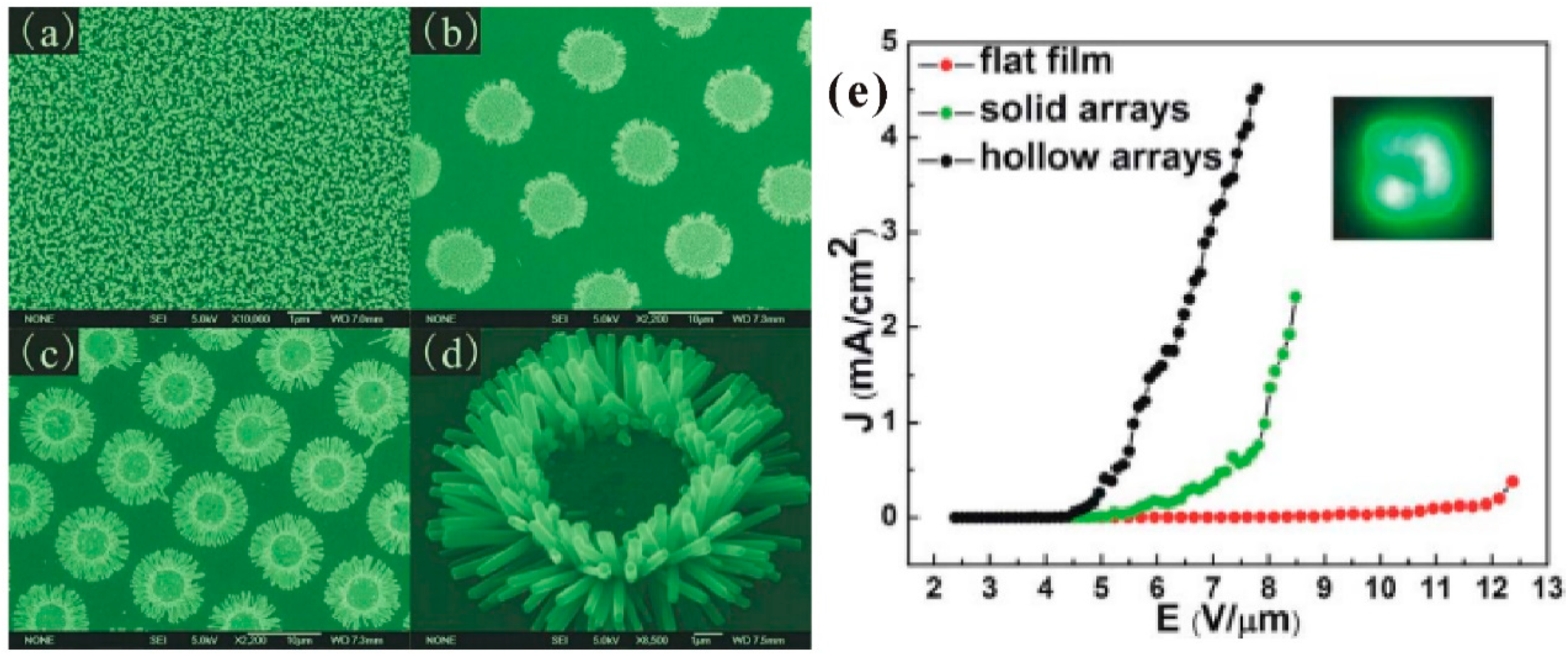
3.1.1. Nanowires Film

| Cathode Materials | Institution | Synthesis Method | Measured Area (cm2) | Turn-On Field (V/μm) | Maximum Current Density (mA/cm2) |
|---|---|---|---|---|---|
| ZnO nanoneedles film [45] | Chinese Academy of Sciences | CVD | 0.005 | ~5.3 | 0.6 |
| ZnO nanowires film [46] | City University of Hong Kong | ~0.008 | 1.1 | 30 | |
| ZnO nanotips film [17] | Zhejiang University | --- | 1 | ~7 | |
| Al doped ZnO nanowires film [17] | --- | 0.5 | >1.2 | ||
| In-doped ZnO nanowires film [18] | Tsinghua University | --- | 2.4 | >1.6 | |
| ZnO nanowires on plate structure [47] | Nanjing University of Science and Technology | 0.01 | 4.8 | 7.8 | |
| Ge-doped ZnO nanowires [20] | Guangzhou Maritime University | ~0.0013 | 3.5–4.1 | 90 | |
| ZnO nanoflowers film [48] | Najran University | 0.25 | ~5 | ~0.075 | |
| ZnO nanowires film [49] | Lanzhou University | --- | <3.79 | ~6 | |
| Al-doped ZnO nanowires film [31,50] | Northwest University | Hydrothermal method | 1 | ~2.5 | 0.3–0.55 |
| ZnO nanorods film [51] | Southeast University | 1 | ~2.5 | ~1 | |
| ZnO nanotubes film [52] | Nanyang Technological University | ~0.2 | ~11 | ~1 | |
| ZnO nanowires film [53] | University of Lyon 1 | ~0.00049 | --- | 50 | |
| ZnO nanowires film [54] | Korea Advanced Institute of Science and Technology | ~16 | 2–2.8 | >1 | |
| Patterned ZnO nanowires [25] | 1 | 1.6–2.45 | >1 | ||
| ZnO nanotapered arrays film [55] | Shanghai Jiao Tong University | 0.25 | 1.5–19.7 | >1 | |
| ZnO nanowires film [26] | Sun Yat-sen University | ~0.008 | 7.1 | ~25 | |
| ZnO nanorods film [56] | Jadavpur University | ~0.008 | 3.2–7.4 | >6 | |
| Patterned ZnO nanowires [35,38,39,40] | Sun Yat-sen University | Thermal oxidation | 1–36 | 4.53–7.8 | 0.35–1.3 |
| Patterned In-doped ZnO nanowires [41] | Sun Yat-sen University | 23 | 7.1 | ~0.84 |
3.1.2. Individual Nanowire
| Cathode Materials | Synthesis Method | Length (μm) | Diameter (nm) | Maximum Current (μA) | Current Density (A/cm2) |
|---|---|---|---|---|---|
| In-doped ZnO nanowire [63] | CVD | ~1.7 | 100 | ~1.5 | 1.9 × 10⁴ |
| ZnO nanowire [63] | --- | ~4.3 | 100 | ~0.75 | 9.5 × 10³ |
| ZnO nanowire [66] | CVD | ~6 | ~100 | ~5 | 6.4 × 10⁴ |
| Agave-like ZnO nanowire [67] | CVD | 30 | 180 | ~1.6 | 6.3 × 10³ |
| Agave-like ZnO nanowire [65] | CVD | 30 | 150 | ~0.9 | 5.1 × 10³ |
| ZnO nanowire [27] | Hydrothermal method | 0.67 | 40 | ~0.017 | 1.4 × 10³ |
| ZnO nanowire [62] | Thermal oxidation | ~2 | ~10 | >1 | 1.3 × 10⁶ |
| ZnO nanowire [68] | Thermal oxidation | 1 | 26 | ~0.4 | 7.5 × 10⁴ |
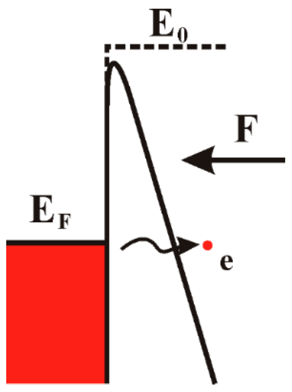
3.2. Mechanism
3.3. Field-Emission Optimization
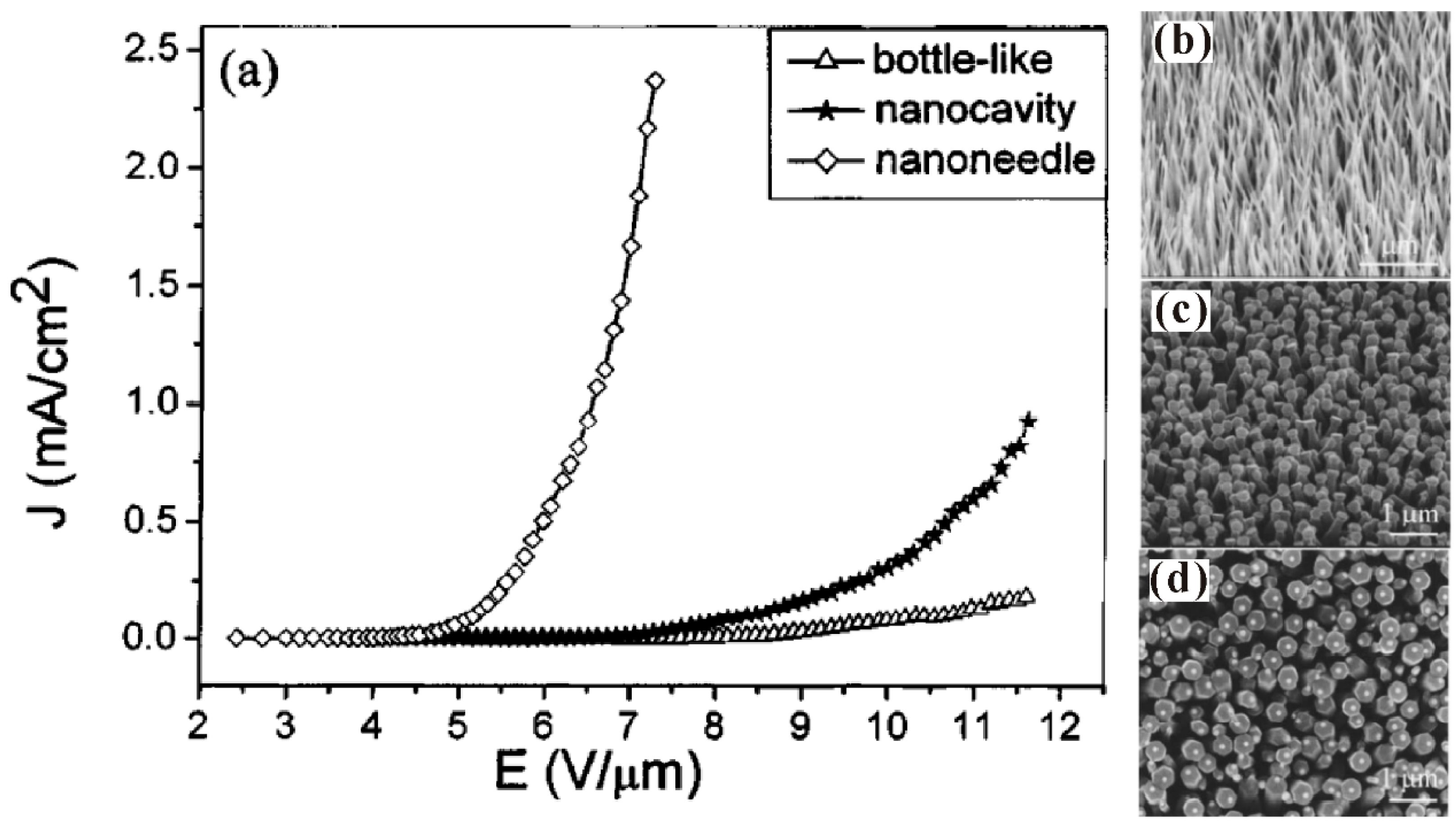
3.3.1. Geometrical Structure
3.3.2. Surface Decoration
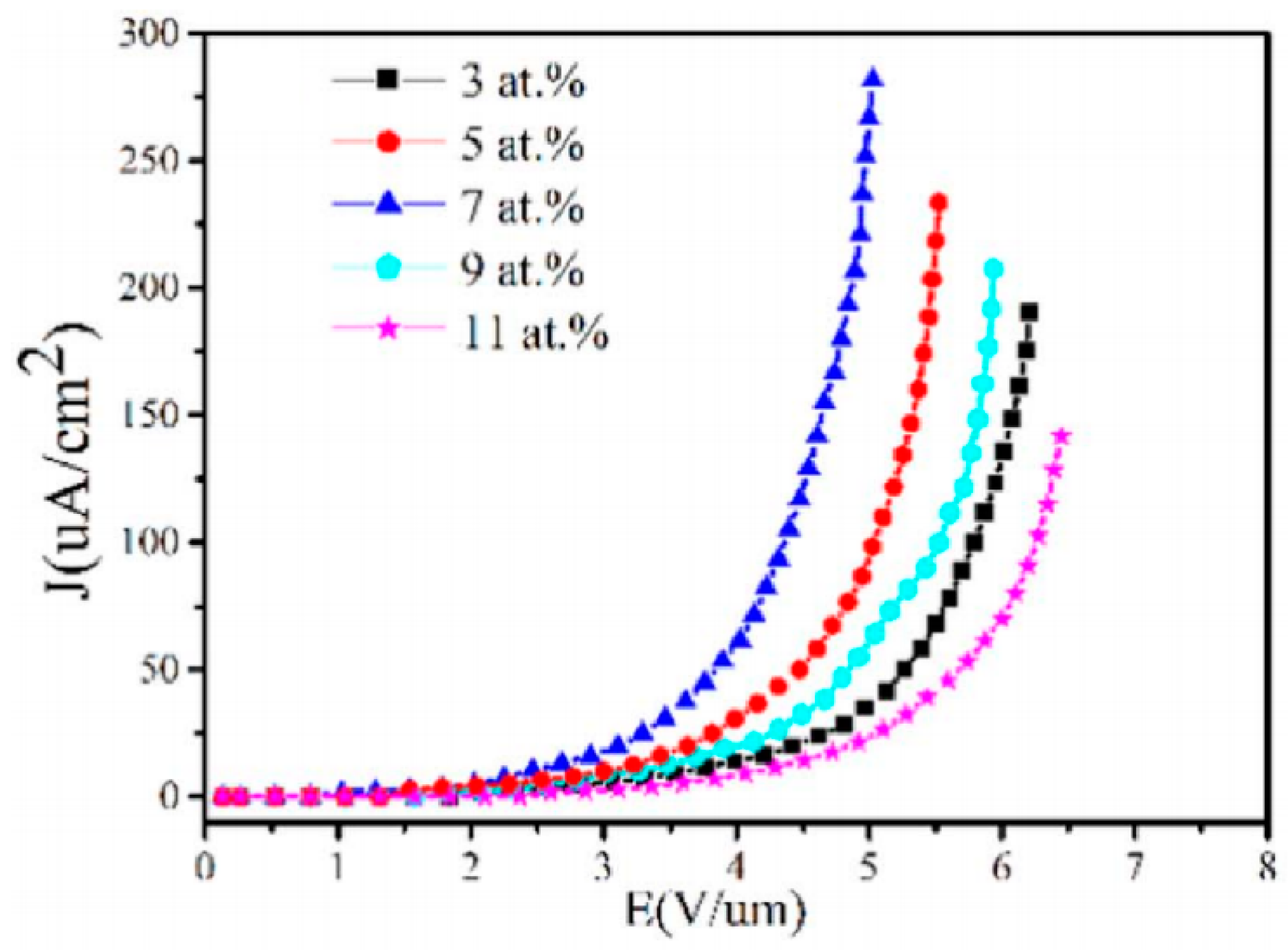
3.3.3. Doping and Back-Contact Resistance
4. Applications
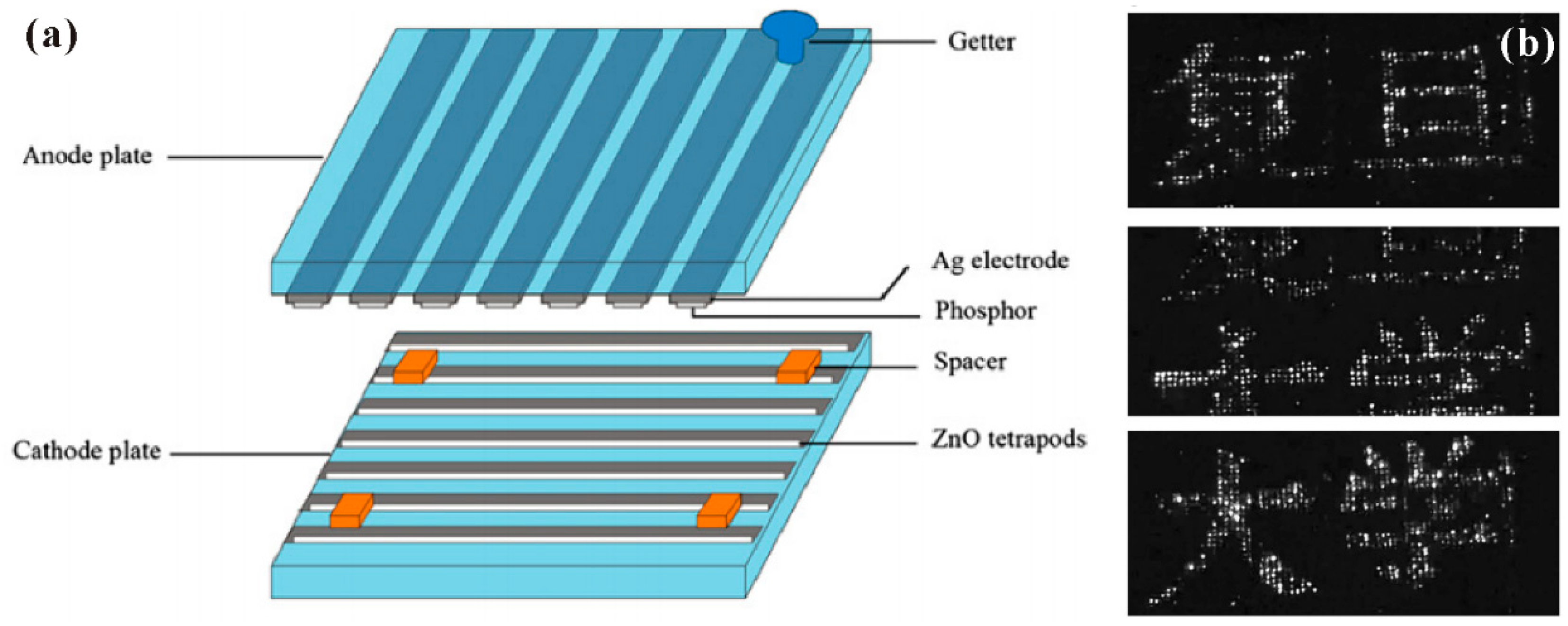
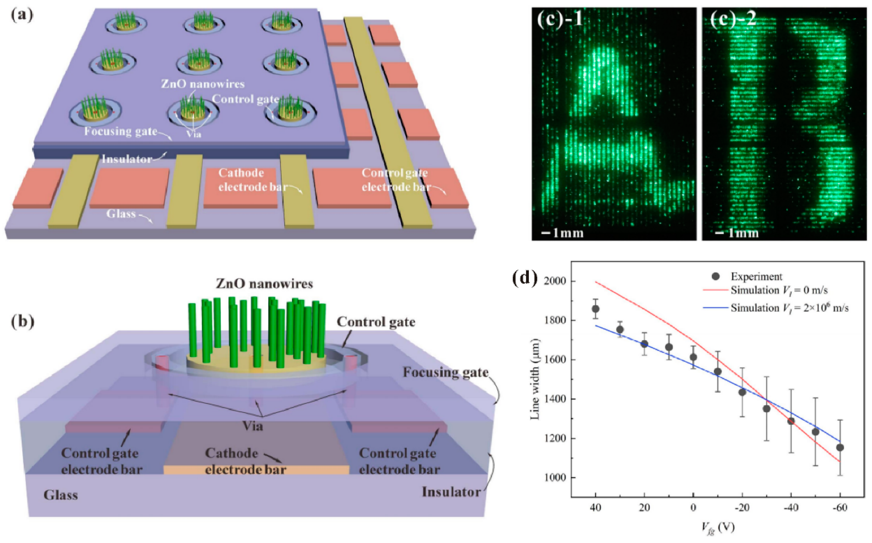
4.1. Field Emission Display (FED)
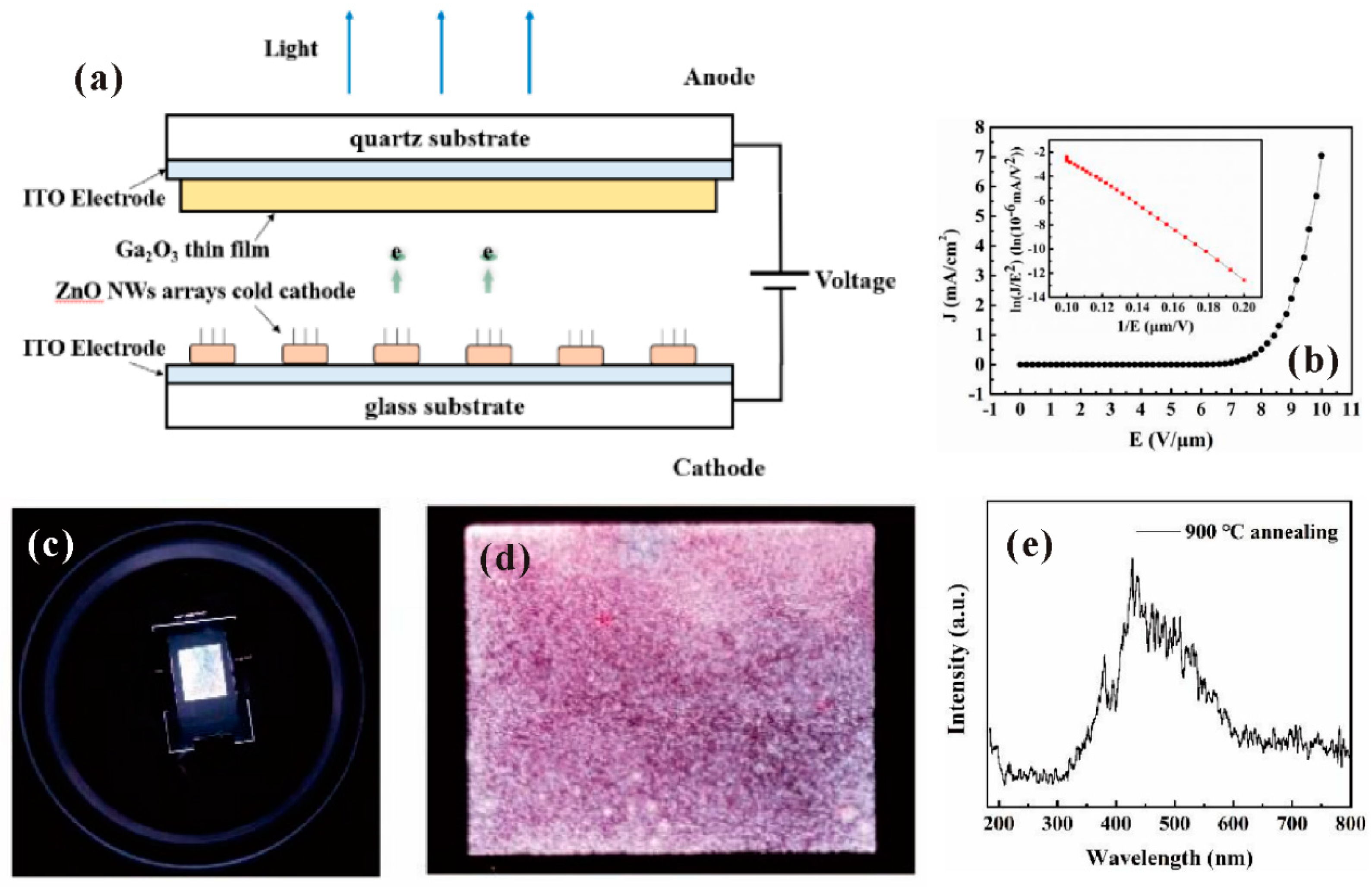
4.2. Illumination
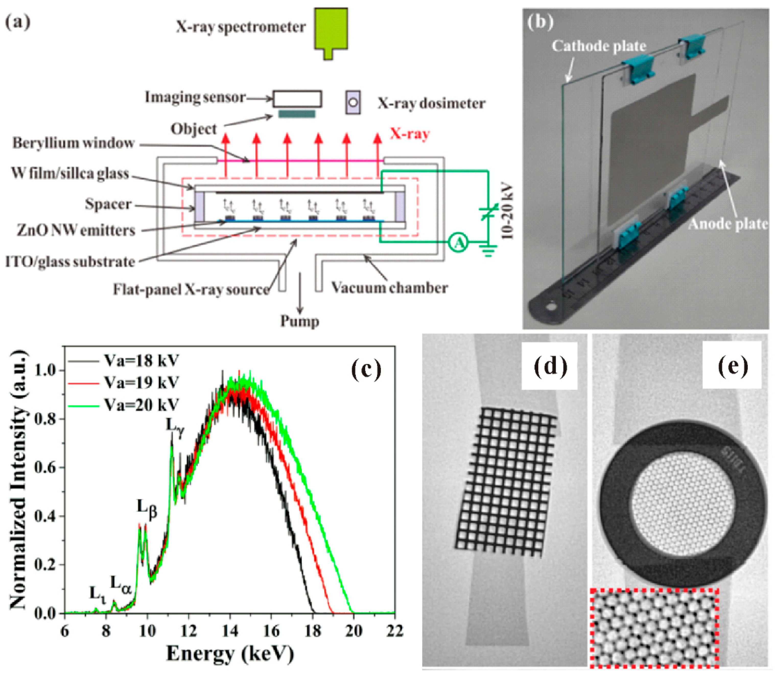
4.3. Flat Panel X-ray Source
4.4. Photodetector
5. Perspectives
Funding
Conflicts of Interest
References
- Choi, W.B.; Chung, D.S.; Kang, J.H.; Kim, H.Y.; Jin, Y.W.; Han, I.T.; Lee, Y.H.; Jung, J.E.; Lee, N.S.; Park, G.S.; et al. Fully sealed, high-brightness carbon-nanotube field-emission display. Appl. Phys. Lett. 1999, 75, 3129–3131. [Google Scholar] [CrossRef] [Green Version]
- Teo, K.B.K.; Chhowalla, M.; Amaratunga, G.A.J.; Milne, W.I.; Legagneux, P.; Pirio, G.; Gangloff, L.; Pribat, D.; Semet, V.; Binh, V.T.; et al. Fabrication and electrical characteristics of carbon nanotube-based microcathodes for use in a parallel electron-beam lithography system. J. Vac. Sci. Technol. B Microelectron. Nanometer Struct. 2003, 21, 693. [Google Scholar] [CrossRef]
- Travish, G.; Rangel, F.J.; Evans, M.A.; Hollister, B.; Schmiedehausen, K. Addressable flat-panel x-ray sources for medical, security, and industrial applications. In Proceedings of the Advances in X-ray/EUV Optics and Components VII, San Diego, CA, USA, 13 August 2012. [Google Scholar]
- Zhang, Z.; Wang, K.; Zheng, K.; Deng, S.; Xu, N.; Chen, J. A flat panel photodetector formed by a ZnS photoconductor and ZnO nanowire field emitters achieving high responsivity from ultraviolet to visible light for indirect-conversion X-ray imaging. J. Light. Technol. 2018, 36, 5010–5015. [Google Scholar] [CrossRef]
- Spindt, C.A. A thin-film field-emission cathode. J. Appl. Phys. 1968, 39, 3504. [Google Scholar] [CrossRef]
- Zhang, H.; Tang, J.; Yuan, J.; Yamauchi, Y.; Suzuki, T.T.; Shinya, N.; Nakajima, K.; Qin, L.-C. An ultrabright and monochromatic electron point source made of a LaB6 nanowire. Nat. Nanotechnol. 2015, 11, 273–279. [Google Scholar] [CrossRef]
- Shen, Y.; Xu, N.; Deng, S.; Zhang, Y.; Liu, F.; Chen, J. A Mo-nanoscrew formed by crystalline Mo-grains with high conductivity and excellent field emission properties. Nanoscale 2014, 6, 4659–4668. [Google Scholar] [CrossRef]
- Sui, M.; Gong, P.; Gu, X. Review on one-dimensional ZnO nanostructures for electron field emitters. Front. Optoelectron. 2013, 6, 386–412. [Google Scholar]
- Young, S.-J.; Yang, C.-C.; Lai, L.-T. Review—Growth of Al-, Ga-, and In-doped ZnO nanostructures via a low-temperature process and their application to field emission devices and ultraviolet photosensors. J. Electrochem. Soc. 2017, 164, B3013–B3028. [Google Scholar] [CrossRef] [Green Version]
- Wang, Z.L. ZnO nanowire and nanobelt platform for nanotechnology. Mater. Sci. Eng. R Rep. 2009, 64, 33–71. [Google Scholar] [CrossRef]
- Zhang, Y.; Ram, M.K.; Stefanakos, E.K.; Goswami, D.Y. Synthesis, characterization, and applications of ZnO nanowires. J. Nanomater. 2012, 2012, 20. [Google Scholar] [CrossRef]
- Heo, Y.W.; Norton, D.P.; Tien, L.C.; Kwon, Y.; Kang, B.S.; Ren, F.; LaRoche, J.R. ZnO nanowire growth and devices. Mater. Sci. Eng. Rep. 2004, 47, 1–47. [Google Scholar] [CrossRef]
- Bagga, S.; Akhtar, J.; Mishra, S. Synthesis and applications of ZnO nanowire: A review. AIP Conf. Proc. 2018, 1989, 020004. [Google Scholar]
- Li, S.; Zhang, X.; Yan, B.; Yu, T. Growth mechanism and diameter control of well-aligned small-diameter ZnO nanowire arrays synthesized by a catalyst-free thermal evaporation method. Nanotechnology 2009, 20, 495604. [Google Scholar] [CrossRef]
- Wang, L.; Zhang, X.; Zhao, S.; Zhou, G.; Zhou, Y.; Qi, J. Synthesis of well-aligned ZnO nanowires by simple physical vapor deposition on c-oriented ZnO thin films without catalysts or additives. Appl. Phys. Lett. 2005, 86, 024108. [Google Scholar] [CrossRef]
- Ashraf, S.; Jones, A.C.; Bacsa, J.; Steiner, A.; Chalker, P.R.; Beahan, P.; Hindley, S.; Odedra, R.; Williams, P.A.; Heys, P.N. MOCVD of vertically aligned ZnO nanowires using bidentate ether adducts of dimethylzinc. Chem. Vap. Depos. 2011, 17, 45–53. [Google Scholar] [CrossRef]
- Zhang, Z.; Huang, J.; He, H.; Lin, S.; Tang, H.; Lu, H.; Ye, Z. The influence of morphologies and doping of nanostructured ZnO on the field emission behaviors. Solid-State Electron. 2009, 53, 578–583. [Google Scholar] [CrossRef]
- Ahmad, M.; Sun, H.; Zhu, J. Enhanced photoluminescence and field-emission behavior of vertically well aligned arrays of in-doped ZnO nanowires. ACS Appl. Mater. Interfaces 2011, 3, 1299–1305. [Google Scholar] [CrossRef] [PubMed]
- Jia, X.; Xu, H.; Gao, J.; Jia, X.; Zhu, H.; Yu, D. Ultralow electron mobility of an individual Cu-doped Zn O nanowire. Phys. Status Solidi 2013, 210, 1217–1220. [Google Scholar] [CrossRef]
- Liang, Y. Ge-doped ZnO nanowire arrays as cold field emitters with excellent performance. Nanotechnology 2019, 30, 375603. [Google Scholar] [CrossRef]
- Li, S.Y.; Lee, C.Y.; Lin, P.; Tseng, T.Y. Gate-controlled ZnO nanowires for field-emission device application. J. Vac. Sci. Technol. Microelectron. Nanometer Struct. 2006, 24, 147–151. [Google Scholar] [CrossRef]
- Ooki, S.; Ohshio, S.; Nishino, J.; Ohkawara, Y.; Ito, H.; Saitoh, H. X-ray source with cold emitter fabricated using ZnO conductive whiskers. Jpn. J. Appl. Phys. 2008, 47, 7303–7307. [Google Scholar] [CrossRef]
- Zheng, K.; Shen, H.; Li, J.; Sun, D.; Chen, G.; Hou, K.; Li, C.; Lei, W. The fabrication and properties of field emission display based on ZnO tetrapod-liked nanostructure. Vacuum 2008, 83, 261–264. [Google Scholar] [CrossRef]
- Zhao, Q.; Huang, C.-K.; Zhu, R.; Xu, J.; Chen, L.; Yu, D. 2D planar field emission devices based on individual ZnO nanowires. Solid State Commun. 2011, 151, 1650–1653. [Google Scholar] [CrossRef]
- Kang, H.W.; Yeo, J.; Hwang, J.O.; Hong, S.; Lee, P.; Han, S.Y.; Lee, J.H.; Rho, Y.S.; Kim, S.O.; Ko, S.H.; et al. Simple ZnO nanowires patterned growth by microcontact printing for high performance field emission device. J. Phys. Chem. 2011, 115, 11435–11441. [Google Scholar] [CrossRef]
- Liu, J.; She, J.; Deng, S.; Chen, J.; Xu, N. Ultrathin seed-layer for tuning density of ZnO nanowire arrays and their field emission characteristics. J. Phys. Chem. 2008, 112, 11685–11690. [Google Scholar] [CrossRef]
- He, H.; She, J.C.; Huang, Y.F.; Deng, S.Z.; Xu, N.S. Precisely-controlled fabrication of single ZnO nanoemitter arrays and their possible application in low energy parallel electron beam exposure. Nanoscale 2012, 4, 2101–2108. [Google Scholar] [CrossRef]
- Hsiao, C.-H.; Huang, C.-S.; Young, S.-J.; Chang, S.-J.; Guo, J.-J.; Liu, C.-W.; Yang, T.-Y. Field-emission and photoelectrical characteristics of Ga–ZnO nanorods photodetector. Trans. Electron Devices 2013, 60, 1905–1910. [Google Scholar] [CrossRef]
- Mahmood, K.; Bin Park, S.; Sung, H.J. Retracted article: Enhanced photoluminescence, raman spectra and field-emission behavior of indium-doped ZnO nanostructures. J. Mater. Chem. 2013, 1, 3138–3149. [Google Scholar] [CrossRef]
- Shao, D.; Gao, J.; Xin, G.; Wang, Y.; Li, L.; Shi, J.; Lian, J.; Koratkar, N.; Sawyer, S. Cl-doped ZnO nanowire arrays on 3D graphene foam with highly efficient field emission and photocatalytic properties. Small 2015, 11, 4785–4792. [Google Scholar] [CrossRef] [PubMed]
- Lv, Y.; Zhang, Z.; Yan, J.; Zhao, W.; Zhai, C. Al doping influences on fabricating ZnO nanowire arrays: Enhanced field emission property. Ceram. Int. 2018, 44, 7454–7460. [Google Scholar] [CrossRef]
- Ma, T.; Guo, M.; Zhang, M.; Zhang, Y.; Wang, X. Density-controlled hydrothermal growth of well-aligned ZnO nanorod arrays. Nanotechnology 2007, 18, 035605. [Google Scholar] [CrossRef] [PubMed]
- Lee, C.Y.; Li, S.Y.; Lin, P.; Tseng, T.-Y. Field-emission triode of low-temperature synthesized ZnO nanowires. Trans. Nanotechnol. 2006, 5, 216–219. [Google Scholar] [CrossRef]
- Zhao, L.; Chen, Y.; Liu, Y.; Zhang, G.; She, J.; Deng, S.; Xu, N.; Chen, J. Integration of ZnO nanowires in gated field emitter arrays for large-area vacuum microelectronics applications. Curr. Appl. Phys. 2017, 17, 85–91. [Google Scholar] [CrossRef]
- Li, Y.; Zhang, Z.; Zhang, G.; Zhao, L.; Deng, S.; Xu, N.; Chen, J. Optimizing the field emission properties of ZnO nanowire arrays by precisely tuning the population density and application in large-area gated field emitter arrays. ACS Appl. Mater. Interfaces 2017, 9, 3911–3921. [Google Scholar] [CrossRef] [PubMed]
- Zhao, L.; Chen, Y.; Zhang, Z.; Cao, X.; Zhang, G.; She, J.; Deng, S.; Xu, N.; Chen, J. Coplanar-gate ZnO nanowire field emitter arrays with enhanced gate-control performance using a ring-shaped cathode. Sci. Rep. 2018, 8, 1–10. [Google Scholar] [CrossRef]
- Cao, X.; Yin, J.; Wang, L.; Zhang, G.; Deng, S.; She, J.; Xu, N.; Chen, J. Fabrication of coaxis-gated ZnO nanowire field-emitter arrays with in-plane focusing gate electrode structure. Trans. Electron Devices 2019, 67, 677–683. [Google Scholar] [CrossRef]
- Zhao, C.X.; Li, Y.F.; Zhou, J.; Li, L.Y.; Deng, S.Z.; Xu, N.S.; Chen, J. Large-scale synthesis of bicrystalline ZnO nanowire arrays by thermal oxidation of zinc film: Growth mechanism and high-performance field emission. Cryst. Growth Des. 2013, 13, 2897–2905. [Google Scholar] [CrossRef]
- Zhang, Z.; Song, X.; Chen, Y.; She, J.; Deng, S.; Xu, N.; Chen, J. Controllable preparation of 1-D and dendritic ZnO nanowires and their large area field-emission properties. J. Alloys Compd. 2017, 690, 304–314. [Google Scholar] [CrossRef]
- Wang, L.; Zhao, Y.; Zheng, K.; She, J.; Deng, S.; Xu, N.; Chen, J. Fabrication of large-area ZnO nanowire field emitter arrays by thermal oxidation for high-current application. Appl. Surf. Sci. 2019, 484, 966–974. [Google Scholar] [CrossRef]
- Zhao, Y.; Chen, Y.; Zhang, G.; Zhan, R.; She, J.; Deng, S.; Chen, J. High current field emission from large-area indium doped ZnO nanowire field emitter arrays for flat-panel X-ray source application. Nanomaterials 2021, 11, 240. [Google Scholar] [CrossRef]
- Lee, C.J.; Lee, T.J.; Lyu, S.C.; Zhang, Y.; Ruh, H.; Lee, H.J. Field emission from well-aligned zinc oxide nanowires grown at low temperature. Appl. Phys. Lett. 2002, 81, 3648–3650. [Google Scholar] [CrossRef]
- Wan, Q.; Yu, K.; Wang, T.H.; Lin, C.L. Low-field electron emission from tetrapod-like ZnO nanostructures synthesized by rapid evaporation. Appl. Phys. Lett. 2003, 83, 2253–2255. [Google Scholar] [CrossRef]
- Zhu, Y.W.; Zhang, H.Z.; Sun, X.C.; Feng, S.Q.; Xu, J.; Zhao, Q.; Yu, D.P. Efficient field emission from ZnO nanoneedle arrays. Appl. Phys. Lett. 2003, 83, 144–146. [Google Scholar] [CrossRef]
- Zhang, Z.; Yuan, H.; Zhou, J.; Liu, N.; Luo, S.; Miao, Y.; Gao, Y.; Wang, J.; Liu, L.; Song, L.; et al. Growth mechanism, photoluminescence, and field-emission properties of ZnO nanoneedle arrays. J. Phys. Chem. 2006, 110, 8566–8569. [Google Scholar] [CrossRef]
- Chen, Z.H.; Tang, Y.B.; Liu, Y.; Yuan, G.D.; Zhang, W.F.; Zapien, J.A.; Bello, I.; Zhang, W.J.; Lee, C.-S.; Lee, S.T. ZnO nanowire arrays grown on Al: ZnO buffer layers and their enhanced electron field emission. J. Appl. Phys. 2009, 106, 064303. [Google Scholar] [CrossRef]
- Song, J.; Kulinich, S.A.; Yan, J.; Li, Z.; He, J.; Kan, C.; Zeng, H. Epitaxial ZnO nanowire-on-nanoplate structures as efficient and transferable field emitters. Adv. Mater. 2013, 25, 5750–5755. [Google Scholar] [CrossRef] [PubMed]
- Umar, A.; Algarni, H.; Kim, S.; Al-Assiri, M.S. Time dependent growth of ZnO nanoflowers with enhanced field emission properties. Ceram. Int. 2016, 42, 13215–13222. [Google Scholar] [CrossRef]
- Chen, S.; Chen, J.; Liu, J.; Qi, J.; Wang, Y. Enhanced field emission from ZnO nanowire arrays utilizing MgO buffer between seed layer and silicon substrate. Appl. Surf. Sci. 2016, 387, 103–108. [Google Scholar] [CrossRef]
- Zhang, Z.; Lv, Y.; Yan, J.; Hui, D.; Yun, J.; Zhai, C.; Zhao, W. Uniform ZnO nanowire arrays: Hydrothermal synthesis, formation mechanism and field emission performance. J. Alloys Compd. 2015, 650, 374–380. [Google Scholar] [CrossRef]
- Chen, J.; Lei, W.; Chai, W.; Zhang, Z.; Li, C.; Zhang, X. High field emission enhancement of ZnO-nanorods via hydrothermal synthesis. Solid-State Electron. 2008, 52, 294–298. [Google Scholar] [CrossRef]
- Wei, A.; Sun, X.W.; Xu, C.X.; Dong, Z.L.; Yu, M.B.; Huang, W. Stable field emission from hydrothermally grown ZnO nanotubes. Appl. Phys. Lett. 2006, 88, 213102. [Google Scholar] [CrossRef]
- Semet, V.; Binh, V.T.; Pauporté, T.; Joulaud, L.; Vermersch, F. Field emission behavior of vertically aligned ZnO nanowire planar cathodes. J. Appl. Phys. 2011, 109, 054301. [Google Scholar] [CrossRef]
- Hwang, J.O.; Lee, D.H.; Kim, J.Y.; Han, T.H.; Kim, B.H.; Park, M.; No, K.; Kim, S.O. Vertical ZnO nanowires/graphene hybrids for transparent and flexible field emission. J. Mater. Chem. 2011, 21, 3432–3437. [Google Scholar] [CrossRef]
- Zhang, J.; Su, Y.; Yang, Z.; Li, M.; Zhang, Y. ZnO nanotapered arrays with successively modulated sharpness via a supersaturation-controlled hydrothermal reaction for efficient field emitters. Trans. Nanotechnol. 2016, 15, 261–267. [Google Scholar] [CrossRef]
- Maiti, U.; Nandy, S.; Karan, S.; Mallik, B.; Chattopadhyay, K. Enhanced optical and field emission properties of CTAB-assisted hydrothermal grown ZnO nanorods. Appl. Surf. Sci. 2008, 254, 7266–7271. [Google Scholar] [CrossRef]
- Li, X.; Wang, Y.; Zhang, Z.; Ou, H.; She, J.; Deng, S.; Xu, N.; Chen, J. Highly stable field emission from ZnO nanowire field emitters controlled by an amorphous indium-gallium-zinc-oxide thin film transistor. Jpn. J. Appl. Phys. 2018, 57, 045003. [Google Scholar] [CrossRef]
- Yang, W.; She, J.; Deng, S.; Xu, N. Field emission from a MOSFET-controlled ZnO-nanowire cold cathode. Trans. Electron Devices 2012, 59, 3641–3646. [Google Scholar] [CrossRef]
- Li, Q.H.; Wan, Q.; Chen, Y.J.; Wang, T.H.; Jia, H.; Yu, D.P. Stable field emission from tetrapod-like ZnO nanostructures. Appl. Phys. Lett. 2004, 85, 636–638. [Google Scholar] [CrossRef]
- Chen, Y.; Luo, S.; Cao, X.; Li, Y.; She, J.; Deng, S.; Chen, J. Stable heating above 900 K in the field emission of ZnO nanowires: Mechanism for achieving high current in large scale field emitter arrays. Adv. Electron. Mater. 2020, 6, 2000624. [Google Scholar] [CrossRef]
- Wang, L.; Xu, Y.; Cao, X.; Huang, J.; Deng, S.; Xu, N.; Chen, J. Diagonal 4-in ZnO nanowire cold cathode flat-panel X-ray source: Preparation and projection imaging properties. Trans. Nucl. Sci. 2021, 68, 338–345. [Google Scholar] [CrossRef]
- Yeong, K.S.; Thong, J.T. Field emission properties of individual zinc oxide nanowire field emitter. J. Vac. Sci. Technol. 2008, 26, 983–989. [Google Scholar] [CrossRef] [Green Version]
- Huang, Y.; Zhang, Y.; Gu, Y.; Bai, X.; Qi, J.; Liao, Q.; Liu, J. Field emission of a single in-doped ZnO nanowire. J. Phys. Chem. 2007, 111, 9039–9043. [Google Scholar] [CrossRef]
- Dong, L.; Jiao, J.; Tuggle, D.W.; Petty, J.M.; Elliff, S.A.; Coulter, M. ZnO nanowires formed on tungsten substrates and their electron field emission properties. Appl. Phys. Lett. 2003, 82, 1096–1098. [Google Scholar] [CrossRef]
- Xiao, Z.M.; Li, Z.B.; Yang, Y.H.; Yang, G.W.; Deng, S.Z.; Xu, N.S.; She, J.C.; Chen, J. Oscillating current observed in field emission from a single zinc oxide nanostructure and the physical mechanism. J. Appl. Phys. 2009, 106, 014310. [Google Scholar] [CrossRef]
- Huang, Y.; Bai, X.; Zhang, Y.; Qi, J.; Gu, Y.; Liao, Q. Field-emission properties of individual ZnO nanowires studied in situ by transmission electron microscopy. J. Phys. Condens. Matter 2007, 19, 176001. [Google Scholar] [CrossRef]
- She, J.; Xiao, Z.; Yang, Y.; Deng, S.; Chen, J.; Yang, G.; Xu, N. Correlation between resistance and field emission performance of individual ZnO one-dimensional nanostructures. ACS Nano 2008, 2, 2015–2022. [Google Scholar] [CrossRef] [PubMed]
- Chen, Y.; Li, Z.; She, J.; Deng, S.; Xu, N.; Chen, J. Field emission characteristics of individual ZnO nanowire before vacuum breakdown. In Proceedings of the International Conference on Vacuum Nanoelectronics, Kyoto, Japan, 9–13 July 2018. [Google Scholar]
- Zhang, X.; Zhang, G.; Bai, X.; Zhao, X.; Xiao, J.; Wu, Y.; Lu, F.; Guo, D. Field emission microscopy study of zinc oxide nanowires on tungsten tip. J. Vac. Sci. Technol. 2009, 27, 705. [Google Scholar] [CrossRef]
- Chen, Y.C.; Deng, S.Z.; Xu, N.S.; Chen, J. Origin of the ring-shaped emission pattern observed from the field emission of ZnO nanowire: Role of adsorbates and electron initial velocity. Mater. Res. Express 2014, 1, 045050. [Google Scholar] [CrossRef]
- Al-Tabbakh, A.A.; More, M.A.; Joag, D.S.; Ramgir, N.S.; Mulla, I.S.; Pillai, V.K. Energy analysis of field emitted electrons from a ZnO tetrapod. Appl. Phys. Lett. 2007, 90, 162102. [Google Scholar] [CrossRef]
- Fowler, R.H.; Nordheim, L. Electron emission in intense electric fields. In Proceedings of the Royal Society of London, London, UK, 1 May 1928. [Google Scholar]
- Al-Tabbakh, A.A.; More, M.A.; Joag, D.S.; Mulla, I.S.; Pillai, V.K. The fowler-nordheim plot behavior and mechanism of field electron emission from ZnO tetrapod structures. ACS Nano 2010, 4, 5585–5590. [Google Scholar] [CrossRef]
- Liu, J.P.; Xu, C.X.; Zhu, G.P.; Li, X.; Cui, Y.P.; Yang, Y.; Sun, X. Hydrothermally grown ZnO nanorods on self-source substrate and their field emission. J. Phys. Appl. Phys. 2007, 40, 1906–1909. [Google Scholar] [CrossRef]
- Zhang, H.Z.; Wang, R.M.; Zhu, Y.W. Effect of adsorbates on field electron emission from ZnO nanoneedle arrays. J. Appl. Phys. 2004, 96, 624–628. [Google Scholar] [CrossRef]
- Zeng, J.Z.; Deng, S.Z.; She, J.C.; He, H.; Xu, N.S. Field-induced hot-electron emission model for wide-band-gap semiconductor nanostructures. J. Appl. Phys. 2010, 108, 054305. [Google Scholar] [CrossRef]
- Murphy, E.L.; Good, R.H. Thermionic emission, field emission, and the transition region. Phys. Rev. 1956, 102, 1464. [Google Scholar] [CrossRef]
- Heo, Y.W.; Tien, L.-C.; Kwon, Y.; Norton, D.P.; Pearton, S.; Kang, B.S.; Ren, F. Depletion-mode ZnO nanowire field-effect transistor. Appl. Phys. Lett. 2004, 85, 2274–2276. [Google Scholar] [CrossRef]
- Yuan, G.-D.; Zhang, W.; Jie, J.; Fan, X.; Tang, J.-X.; Shafiq, I.; Ye, Z.-Z.; Lee, C.-S.; Lee, S.-T. Tunable n-type conductivity and transport properties of Ga-doped ZnO nanowire arrays. Adv. Mater. 2007, 20, 168–173. [Google Scholar] [CrossRef]
- Stiegler, J.; Tena-Zaera, R.; Idigoras, O.; Chuvilin, A.; Hillenbrand, R. Correlative infrared-electron nanoscopy reveals the local structure–conductivity relationship in zinc oxide nanowires. Nat. Commun. 2012, 3, 1131. [Google Scholar] [CrossRef] [PubMed]
- Chen, Y.; Song, X.; Li, Z.; She, J.; Deng, S.; Xu, N.; Chen, J. Penetration length-dependent hot electrons in the field emission from ZnO nanowires. Appl. Surf. Sci. 2018, 427, 573–580. [Google Scholar] [CrossRef]
- Chen, Y.; Zhang, Z.; Li, Z.-B.; She, J.; Deng, S.; Xu, N.-S.; Chen, J. Investigation of the temperature dependent field emission from individual ZnO nanowires for evidence of field-induced hot electrons emission. J. Phys. Condens. Matter 2018, 30, 315002. [Google Scholar] [CrossRef]
- Dardona, S.; Peles, A.; Wrobel, G.; Piech, M.; Gao, P.-X. Gas adsorption and high-emission current induced degradation of field emission characteristics in solution-processed ZnO nanoneedles. J. Appl. Phys. 2010, 108, 124318. [Google Scholar] [CrossRef]
- Huang, N.Y.; She, J.C.; Chen, J.; Deng, S.Z.; Xu, N.S.; Bishop, H.; Huq, S.E.; Wang, L.; Zhong, D.; Wang, E.G.; et al. Mechanism responsible for initiating carbon nanotube vacuum breakdown. Phys. Rev. Lett. 2004, 93, 075501. [Google Scholar] [CrossRef] [Green Version]
- Zhao, Q.; Zhang, H.; Zhu, Y.W.; Feng, S.Q.; Sun, X.C.; Xu, J.; Yu, D.P. Morphological effects on the field emission of ZnO nanorod arrays. Appl. Phys. Lett. 2005, 86, 203115. [Google Scholar] [CrossRef]
- Pan, N.; Xue, H.; Yu, M.; Cui, X.; Wang, X.; Hou, J.G.; Huang, J.; Deng, S.Z. Tip-morphology-dependent field emission from ZnO nanorod arrays. Nanotechnology 2010, 21, 225707. [Google Scholar] [CrossRef] [PubMed]
- Ye, Z.; Yang, F.; Lu, Y.; Zhi, M.; Tang, H.; Zhu, L. ZnO nanorods with different morphologies and their field emission properties. Solid State Commun. 2007, 142, 425–428. [Google Scholar] [CrossRef]
- Xiao, J.; Zhang, X.; Zhang, G. Field emission from zinc oxide nanotowers: The role of the top morphology. Nanotechnology 2008, 19, 295706. [Google Scholar] [CrossRef]
- Yang, Y.H.; Wang, B.; Xu, N.S.; Yang, G.W. Field emission of one-dimensional micro- and nanostructures of zinc oxide. Appl. Phys. Lett. 2006, 89, 43108. [Google Scholar] [CrossRef]
- Liu, N.; Fang, G.; Zeng, W.; Long, H.; Yuan, L.; Zhao, X. Diminish the screen effect in field emission via patterned and selective edge growth of ZnO nanorod arrays. Appl. Phys. Lett. 2009, 95, 153505. [Google Scholar] [CrossRef]
- He, J.; Zheng, X.; Hong, X.; Wang, W.; Cao, Y.; Chen, T.; Kong, L.; Wu, Y.; Wu, Z.; Kang, J. Enhanced field emission of ZnO nanowire arrays by the control of their structures. Mater. Lett. 2018, 216, 182–184. [Google Scholar] [CrossRef]
- Liao, L.; Li, J.C.; Wang, D.F.; Liu, C.S.; Fu, Q.; Fan, L.X. Field emission property improvement of ZnO nanowires coated with amorphous carbon and carbon nitride films. Nanotechnology 2005, 16, 985–989. [Google Scholar] [CrossRef]
- Sankaran, K.J.; Afsal, M.; Lou, S.-C.; Chen, H.-C.; Chen, C.; Lee, C.-Y.; Chen, L.-J.; Tai, N.-H.; Lin, I.-N. Electron field emission enhancement of vertically aligned ultrananocrystalline diamond-coated ZnO core-shell heterostructured nanorods. Small 2013, 10, 179–185. [Google Scholar] [CrossRef]
- Yuan, L.; Fang, G.; Li, C.; Li, J.; Wang, M.; Liu, N.; Zhao, X. Field emission enhancement of ZnO nanorod arrays with hafnium nitride coating. Surf. Coat. Technol. 2008, 202, 3480–3484. [Google Scholar] [CrossRef]
- Zhao, C.; Li, Y.; Chen, J.; Deng, S.; Xu, N. Tunable field emission characteristics of ZnO nanowires coated with varied thickness of lanthanum boride thin films. Ultramicroscopy 2013, 132, 36–40. [Google Scholar] [CrossRef] [PubMed]
- Maiti, U.N.; Maiti, S.; Majumder, T.P.; Chattopadhyay, K.K. Ultra-thin graphene edges at the nanowire tips: A cascade cold cathode with two-stage field amplification. Nanotechnology 2011, 22, 505703. [Google Scholar] [CrossRef]
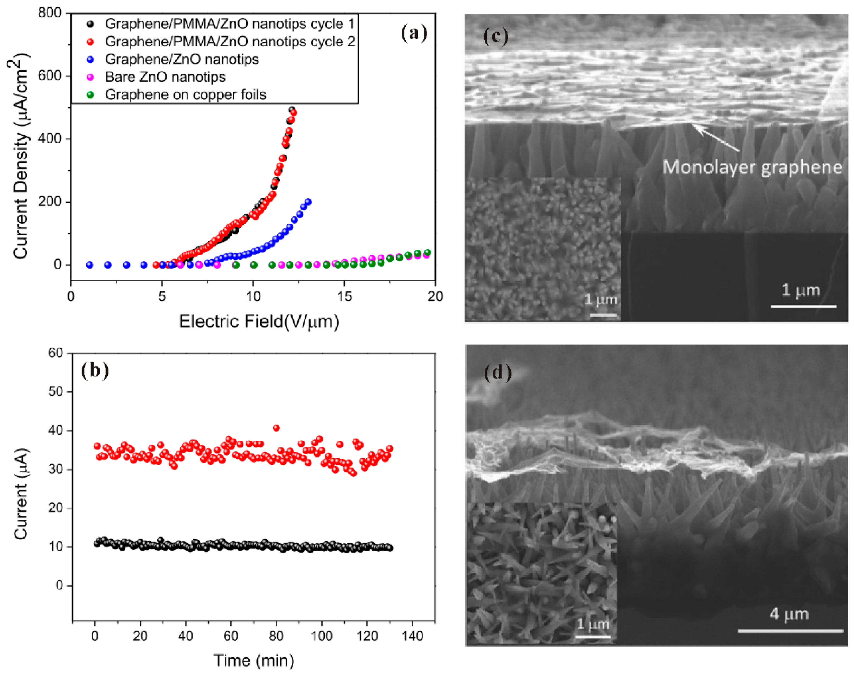
- Yang, Z.; Zhao, Q.; Ou, Y.; Wang, W.; Li, H.; Yu, D. Enhanced field emission from large scale uniform monolayer graphene supported by well-aligned ZnO nanowire arrays. Appl. Phys. 2012, 101, 173107. [Google Scholar] [CrossRef]
- Yang, T.-H.; Chiu, K.-C.; Harn, Y.-W.; Chen, H.-Y.; Cai, R.-F.; Shyue, J.-J.; Lo, S.-C.; Wu, J.-M.; Lee, Y.-H. Electron field emission of geometrically modulated monolayer semiconductors. Adv. Funct. Mater. 2017, 28, 1706113. [Google Scholar] [CrossRef]
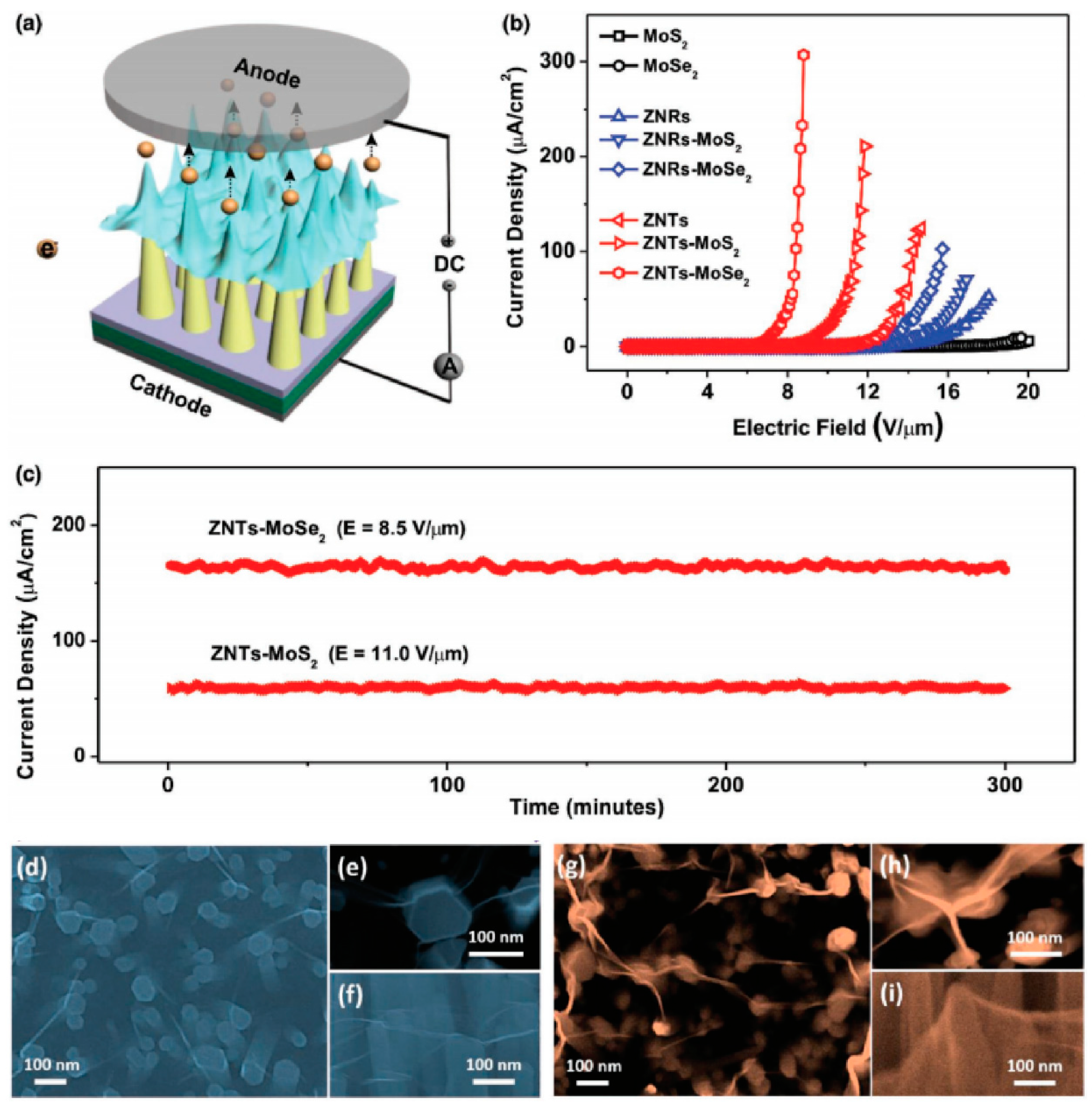
- Chen, Y.; Liu, L.; Zheng, K.; She, J.; Deng, S.; Xu, N.; Chen, J. Highly stable field emission from a tungsten diselenide monolayer on zinc oxide nanowire by geometrically modulating hot electrons. Adv. Electron. Mater. 2019, 5, 1900128. [Google Scholar] [CrossRef]
- Huang, Z.; Huang, Y.; Xu, N.; Chen, J.; She, J.; Deng, S. Band-to-band tunneling-dominated thermo-enhanced field electron emission from p-Si/ZnO nanoemitters. ACS Appl. Mater. Interfaces 2018, 10, 21518–21526. [Google Scholar] [CrossRef]
- Song, Z.; Wei, H.; Liu, Y.; Wang, J.; Long, H.; Wang, H.; Qin, P.; Zeng, W.; Fang, G. Enhanced field emission from aligned ZnO nanowires grown on a graphene layer with hydrothermal method. Trans. Nanotechnol. 2014, 13, 167–171. [Google Scholar] [CrossRef]
- Liu, J.; Zhang, Z.; Lv, Y.; Yan, J.; Yun, J.; Zhao, W.; Kou, L.; Zhai, C. Synthesis and characterization of ZnO NWAs/graphene composites for enhanced optical and field emission performances. Compos. Eng. 2016, 99, 366–372. [Google Scholar] [CrossRef]
- Ding, S.; Zhou, Y.; Ye, M.; Lei, W. Stable field emission from ZnO nanowires grown on 3D graphene foam. Vacuum 2017, 139, 33–36. [Google Scholar] [CrossRef]
- Wu, J.; Chen, L.; Li, S.; Du, C.; Zhang, Q.; Zheng, C.; Xu, J.; Song, K. Improved field emission performances for graphene/ZnO nanowires/graphene sandwich composites. Mater. Lett. 2018, 213, 391–393. [Google Scholar] [CrossRef]
- Liu, Y.; Zhao, L.; Zhang, Z.; Chen, D.; Zhang, G.; She, J.; Deng, S.; Xu, N.; Chen, J. Fabrication of ZnO nanowire field-emitter arrays with focusing capability. Trans. Electron Devices 2018, 65, 1982–1987. [Google Scholar] [CrossRef]
- Chen, Y.; Hu, L.; Song, H.; Jiang, H.; Li, D.; Miao, G.; Li, Z.; Sun, X.; Zhang, Z.; Guo, T. Optimized performances of tetrapod-like ZnO nanostructures for a triode structure field emission planar light source. Nanoscale 2014, 6, 13544–13549. [Google Scholar] [CrossRef]
- Xu, J.; Zhang, Y.; Deng, S.; Chen, J.; Xu, N. 10 inch screen printed ZnO nanowire cold cathode for flat panel light source. In Proceedings of the International Vacuum Nanoelectronics Conference, Roanoke, VA, USA, 8–12 July 2013. [Google Scholar]
- Yin, J.; Chen, M.; Wang, L.; Cao, X.; She, J.; Deng, S.; Xu, N.; Chen, J. Cathodoluminescent properties of polycrystalline Ga2O3 thin film and its application UV flat panel light source. In Proceedings of the 33rd International Vacuum Nanoelectronics Conference, Lyon, France, 6–10 July 2020. [Google Scholar]
- Chen, D.; Song, X.; Zhang, Z.; Li, Z.; She, J.; Deng, S.; Chen, J. Transmission type flat-panel X-ray source using ZnO nanowire field emitters. Appl. Phys. Lett. 2015, 107, 243105. [Google Scholar] [CrossRef]
- Chen, D.; Xu, Y.; Zhang, G.; Zhang, Z.; She, J.; Deng, S.; Chen, J. A double-sided radiating flat-panel X-ray source using ZnO nanowire field emitters. Vacuum 2017, 144, 266–271. [Google Scholar] [CrossRef]
- Cao, X.; Zhang, G.; Zhao, Y.; Xu, Y.; She, J.; Deng, S.; Chen, J. Fully vacuum-sealed addressable nanowire cold cathode flat-panel X-ray source. Appl. Phys. Lett. 2021, 119, 053501. [Google Scholar] [CrossRef]
- Zhang, Z.; Wang, K.; Zheng, K.; Deng, S.; Xu, N.; Chen, J. Electron bombardment induced photoconductivity and high gain in a flat panel photodetector based on a ZnS photoconductor and ZnO nanowire field emitters. ACS Photonics 2018, 5, 4147–4155. [Google Scholar] [CrossRef]
- Chen, Y.; Zhang, Z.; Jiang, H.; Li, Z.; Miao, G.; Song, H.; Guo, T. Realization of an efficient electron source by ultraviolet-light-assisted field emission from a one-dimensional ZnO nanorods/n-GaN heterostructure photoconductive detector. Nanoscale 2019, 11, 1351–1359. [Google Scholar] [CrossRef]
- Zhang, Z.; Zheng, W.; Wang, K.; Chen, H.; Deng, S.; Chen, J. Sensitive and fast direct conversion x-ray detectors based on single-crystalline HgI2 photoconductor and ZnO nanowire vacuum diode. Adv. Mater. Technol. 2020, 5, 1901108. [Google Scholar] [CrossRef]


Publisher’s Note: MDPI stays neutral with regard to jurisdictional claims in published maps and institutional affiliations. |
© 2021 by the authors. Licensee MDPI, Basel, Switzerland. This article is an open access article distributed under the terms and conditions of the Creative Commons Attribution (CC BY) license (https://creativecommons.org/licenses/by/4.0/).
Share and Cite
Chen, Y.; Deng, S.; Xu, N.; Chen, J. Recent Progress on ZnO Nanowires Cold Cathode and Its Applications. Nanomaterials 2021, 11, 2150. https://doi.org/10.3390/nano11082150
Chen Y, Deng S, Xu N, Chen J. Recent Progress on ZnO Nanowires Cold Cathode and Its Applications. Nanomaterials. 2021; 11(8):2150. https://doi.org/10.3390/nano11082150
Chicago/Turabian StyleChen, Yicong, Shaozhi Deng, Ningsheng Xu, and Jun Chen. 2021. "Recent Progress on ZnO Nanowires Cold Cathode and Its Applications" Nanomaterials 11, no. 8: 2150. https://doi.org/10.3390/nano11082150
APA StyleChen, Y., Deng, S., Xu, N., & Chen, J. (2021). Recent Progress on ZnO Nanowires Cold Cathode and Its Applications. Nanomaterials, 11(8), 2150. https://doi.org/10.3390/nano11082150