
Effect of Device Scaling on Electron Mobility in Nanoscale GaN HEMTs with Polarization Charge Modulation

Abstract
:1. Introduction
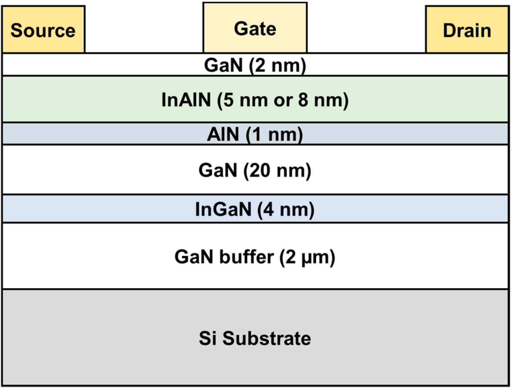
2. Experiment
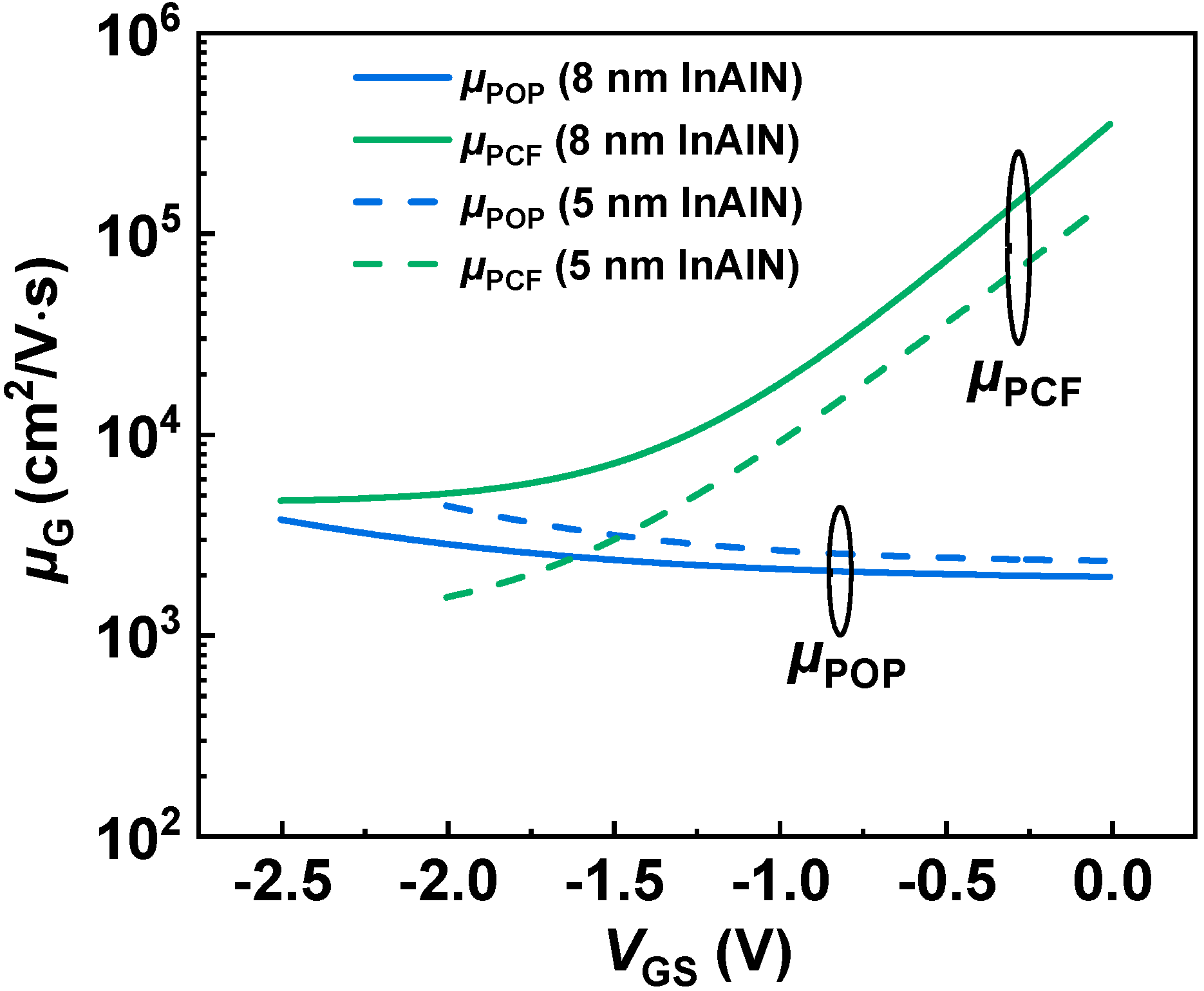
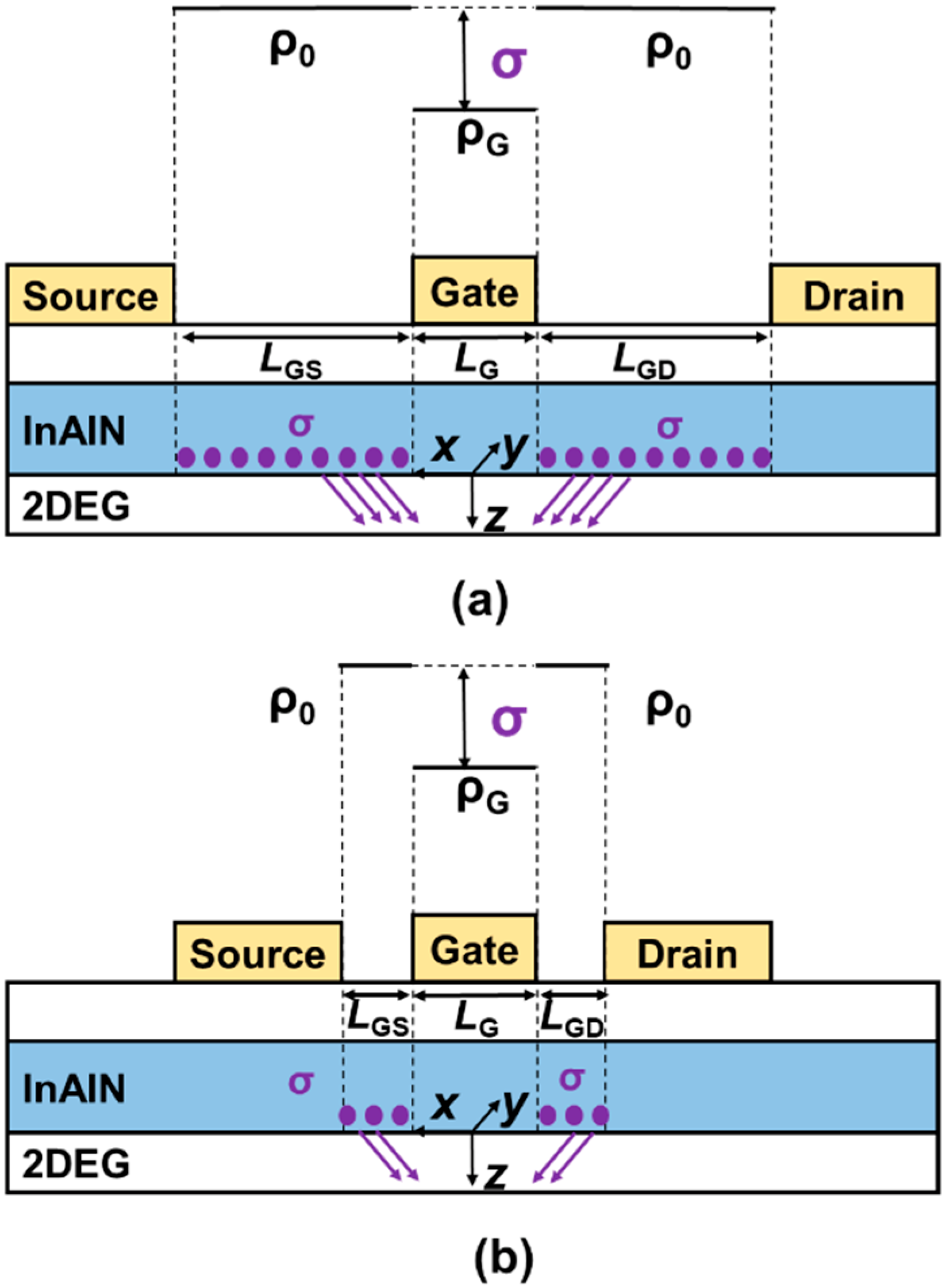
3. Results and Discussion
4. Conclusions
Author Contributions
Funding
Institutional Review Board Statement
Informed Consent Statement
Data Availability Statement
Conflicts of Interest
References
- Hamza, K.H.; Nirmal, D. A review of GaN HEMT broadband power amplifiers. AEU—Int. J. Electron. Commun. 2020, 116, 153040. [Google Scholar] [CrossRef]
- Ma, C.-T.; Gu, Z.-H. Review of GaN HEMT applications in power converters over 500 W. Electronics 2019, 8, 1401. [Google Scholar] [CrossRef] [Green Version]
- Keshmiri, N.; Wang, D.; Agrawal, B.; Hou, R.; Emadi, A. Current status and future trends of GaN HEMTs in electrified transportation. IEEE Access 2020, 8, 70553–70571. [Google Scholar] [CrossRef]
- Li, L.; Nomoto, K.; Pan, M.; Li, W.; Hickman, A.; Miller, J.; Lee, K.; Hu, Z.; Bader, S.J.; Lee, S.M. GaN HEMTs on Si with regrown contacts and cutoff/maximum oscillation frequencies of 250/204 GHz. IEEE Electron Device Lett. 2020, 41, 689–692. [Google Scholar] [CrossRef]
- Cui, P.; Mercante, A.; Lin, G.; Zhang, J.; Yao, P.; Prather, D.W.; Zeng, Y. High-performance InAlN/GaN HEMTs on silicon substrate with high fT× Lg. Appl. Phys. Express 2019, 12, 104001. [Google Scholar] [CrossRef]
- Tang, Y.; Shinohara, K.; Regan, D.; Corrion, A.; Brown, D.; Wong, J.; Schmitz, A.; Fung, H.; Kim, S.; Micovic, M. Ultrahigh-Speed GaN High-Electron-Mobility Transistors With fT/fmax of 454/444 GHz. IEEE Electron Device Lett. 2015, 36, 549–551. [Google Scholar] [CrossRef]
- Kim, J.-G.; Cho, C.; Kim, E.; Hwang, J.S.; Park, K.-H.; Lee, J.-H. High breakdown voltage and low-current dispersion in AlGaN/GaN HEMTs with high-quality AlN buffer layer. IEEE Trans. Electron Devices 2021, 68, 1513–1517. [Google Scholar] [CrossRef]
- Xia, X.; Guo, Z.; Sun, H. Study of Normally-Off AlGaN/GaN HEMT with Microfield Plate for Improvement of Breakdown Voltage. Micromachines 2021, 12, 1318. [Google Scholar] [CrossRef]
- Reddeppa, M.; Park, B.-G.; Pasupuleti, K.S.; Nam, D.-J.; Kim, S.-G.; Oh, J.-E.; Kim, M.-D. Current–voltage characteristics and deep-level study of GaN nanorod Schottky-diode-based photodetector. Semicond. Sci. Technol. 2021, 36, 035010. [Google Scholar] [CrossRef]
- Pasupuleti, K.S.; Reddeppa, M.; Park, B.-G.; Oh, J.-E.; Kim, S.-G.; Kim, M.-D. Efficient Charge Separation in Polypyrrole/GaN-Nanorod-Based Hybrid Heterojunctions for High-Performance Self-Powered UV Photodetection. Phys. Status Solidi (RRL)—Rapid Res. Lett. 2021, 15, 2000518. [Google Scholar] [CrossRef]
- Schuette, M.L.; Ketterson, A.; Song, B.; Beam, E.; Chou, T.-M.; Pilla, M.; Tserng, H.-Q.; Gao, X.; Guo, S.; Fay, P.J. Gate-recessed integrated E/D GaN HEMT technology with fT/fmax > 300 GHz. IEEE Electron Device Lett. 2013, 34, 741–743. [Google Scholar] [CrossRef]
- Downey, B.P.; Meyer, D.J.; Katzer, D.S.; Roussos, J.A.; Pan, M.; Gao, X. SiNx/InAlN/AlN/GaN MIS-HEMTs With 10.8 THz⋅V Johnson Figure of Merit. IEEE Electron Device Lett. 2014, 35, 527–529. [Google Scholar] [CrossRef]
- Jessen, G.H.; Fitch, R.C.; Gillespie, J.K.; Via, G.; Crespo, A.; Langley, D.; Denninghoff, D.J.; Trejo, M.; Heller, E.R. Short-channel effect limitations on high-frequency operation of AlGaN/GaN HEMTs for T-Gate devices. IEEE Trans. Electron Devices 2007, 54, 2589–2597. [Google Scholar] [CrossRef]
- Shinohara, K.; Regan, D.C.; Tang, Y.; Corrion, A.L.; Brown, D.F.; Wong, J.C.; Robinson, J.F.; Fung, H.H.; Schmitz, A.; Oh, T.C. Scaling of GaN HEMTs and Schottky diodes for submillimeter-wave MMIC applications. IEEE Trans. Electron Devices 2013, 60, 2982–2996. [Google Scholar] [CrossRef]
- Shinohara, K.; Regan, D.; Milosavljevic, I.; Corrion, A.; Brown, D.; Willadsen, P.; Butler, C.; Schmitz, A.; Kim, S.; Lee, V. Electron velocity enhancement in laterally scaled GaN DH-HEMTs with fT of 260 GHz. IEEE Electron Device Lett. 2011, 32, 1074–1076. [Google Scholar] [CrossRef]
- Shinohara, K.; Regan, D.; Corrion, A.; Brown, D.; Burnham, S.; Willadsen, P.; Alvarado-Rodriguez, I.; Cunningham, M.; Butler, C.; Schmitz, A. Deeply-scaled self-aligned-gate GaN DH-HEMTs with ultrahigh cutoff frequency. In Proceedings of the 2011 International Electron Devices Meeting, Washington, DC, USA, 5–7 December 2011; pp. 11–14. [Google Scholar]
- Medjdoub, F.; Alomari, M.; Carlin, J.-F.; Gonschorek, M.; Feltin, E.; Py, M.; Grandjean, N.; Kohn, E. Barrier-layer scaling of InAlN/GaN HEMTs. IEEE Electron Device Lett. 2008, 29, 422–425. [Google Scholar] [CrossRef]
- Lee, D.S.; Lu, B.; Azize, M.; Gao, X.; Guo, S.; Kopp, D.; Fay, P.; Palacios, T. Impact of GaN channel scaling in InAlN/GaN HEMTs. In Proceedings of the 2011 International Electron Devices Meeting, Washington, DC, USA, 5–7 December 2011; pp. 11–14. [Google Scholar]
- Ambacher, O.; Foutz, B.; Smart, J.; Shealy, J.; Weimann, N.; Chu, K.; Murphy, M.; Sierakowski, A.; Schaff, W.; Eastman, L. Two dimensional electron gases induced by spontaneous and piezoelectric polarization in undoped and doped AlGaN/GaN heterostructures. J. Appl. Phys. 2000, 87, 334–344. [Google Scholar] [CrossRef]
- Yu, E.; Sullivan, G.; Asbeck, P.; Wang, C.; Qiao, D.; Lau, S. Measurement of piezoelectrically induced charge in GaN/AlGaN heterostructure field-effect transistors. Appl. Phys. Lett. 1997, 71, 2794–2796. [Google Scholar] [CrossRef] [Green Version]
- Luan, C.; Lin, Z.; Lv, Y.; Zhao, J.; Wang, Y.; Chen, H.; Wang, Z. Theoretical model of the polarization Coulomb field scattering in strained AlGaN/AlN/GaN heterostructure field-effect transistors. J. Appl. Phys. 2014, 116, 044507. [Google Scholar] [CrossRef]
- Cui, P.; Mo, J.; Fu, C.; Lv, Y.; Liu, H.; Cheng, A.; Luan, C.; Zhou, Y.; Dai, G.; Lin, Z. Effect of Different Gate Lengths on Polarization Coulomb Field Scattering Potential in AlGaN/GaN Heterostructure Field-Effect Transistors. Sci. Rep. 2018, 8, 9036. [Google Scholar] [CrossRef]
- Lin, Z.; Zhao, J.; Corrigan, T.D.; Wang, Z.; You, Z.; Wang, Z.; Lu, W. The influence of Schottky contact metals on the strain of AlGaN barrier layers. J. Appl. Phys. 2008, 103, 044503. [Google Scholar] [CrossRef]
- Guo, L.; Wang, X.; Wang, C.; Xiao, H.; Ran, J.; Luo, W.; Wang, X.; Wang, B.; Fang, C.; Hu, G. The influence of 1 nm AlN interlayer on properties of the Al0.3Ga0.7N/AlN/GaN HEMT structure. Microelectron. J. 2008, 39, 777–781. [Google Scholar] [CrossRef]
- Ibbetson, J.P.; Fini, P.; Ness, K.; DenBaars, S.; Speck, J.; Mishra, U. Polarization effects, surface states, and the source of electrons in AlGaN/GaN heterostructure field effect transistors. Appl. Phys. Lett. 2000, 77, 250–252. [Google Scholar] [CrossRef]
- Goyal, N.; Fjeldly, T.A. Analytical modeling of AlGaN/AlN/GaN heterostructures including effects of distributed surface donor states. Appl. Phys. Lett. 2014, 105, 023508. [Google Scholar] [CrossRef]
- Gurusinghe, M.; Davidsson, S.; Andersson, T. Two-dimensional electron mobility limitation mechanisms in AlxGa1−xN/GaN heterostructures. Phys. Rev. B 2005, 72, 045316. [Google Scholar] [CrossRef]
- Fang, T.; Wang, R.; Xing, H.; Rajan, S.; Jena, D. Effect of optical phonon scattering on the performance of GaN transistors. IEEE Electron Device Lett. 2012, 33, 709–711. [Google Scholar] [CrossRef] [Green Version]
- Kordoš, P.; Gregušová, D.; Stoklas, R.; Čičo, K.; Novák, J. Improved transport properties of Al2O3/AlGaN/GaN metal-oxide-semiconductor heterostructure field-effect transistor. Appl. Phys. Lett. 2007, 90, 123513. [Google Scholar] [CrossRef]
- Cui, P.; Lv, Y.; Fu, C.; Liu, H.; Cheng, A.; Luan, C.; Zhou, Y.; Lin, Z. Effect of Polarization Coulomb Field Scattering on Electrical Properties of the 70-nm Gate-Length AlGaN/GaN HEMTs. Sci. Rep. 2018, 8, 12850. [Google Scholar] [CrossRef]
- Cui, P.; Liu, H.; Lin, W.; Lin, Z.; Cheng, A.; Yang, M.; Liu, Y.; Fu, C.; Lv, Y.; Luan, C. Influence of different gate biases and gate lengths on parasitic source access resistance in AlGaN/GaN heterostructure FETs. IEEE Trans. Electron Devices 2017, 64, 1038–1044. [Google Scholar] [CrossRef]
- Anwar, A.; Webster, R.T.; Smith, K.V. Bias induced strain in AlGaN/GaN heterojunction field effect transistors and its implications. Appl. Phys. Lett. 2006, 88, 203510. [Google Scholar] [CrossRef] [Green Version]


Publisher’s Note: MDPI stays neutral with regard to jurisdictional claims in published maps and institutional affiliations. |
© 2022 by the authors. Licensee MDPI, Basel, Switzerland. This article is an open access article distributed under the terms and conditions of the Creative Commons Attribution (CC BY) license (https://creativecommons.org/licenses/by/4.0/).
Share and Cite
Cui, P.; Zeng, Y. Effect of Device Scaling on Electron Mobility in Nanoscale GaN HEMTs with Polarization Charge Modulation. Nanomaterials 2022, 12, 1718. https://doi.org/10.3390/nano12101718
Cui P, Zeng Y. Effect of Device Scaling on Electron Mobility in Nanoscale GaN HEMTs with Polarization Charge Modulation. Nanomaterials. 2022; 12(10):1718. https://doi.org/10.3390/nano12101718
Chicago/Turabian StyleCui, Peng, and Yuping Zeng. 2022. "Effect of Device Scaling on Electron Mobility in Nanoscale GaN HEMTs with Polarization Charge Modulation" Nanomaterials 12, no. 10: 1718. https://doi.org/10.3390/nano12101718
APA StyleCui, P., & Zeng, Y. (2022). Effect of Device Scaling on Electron Mobility in Nanoscale GaN HEMTs with Polarization Charge Modulation. Nanomaterials, 12(10), 1718. https://doi.org/10.3390/nano12101718