
Effects of Post-UV/Ozone Treatment on Electrical Characteristics of Solution-Processed Copper Oxide Thin-Film Transistors


Abstract
:1. Introduction
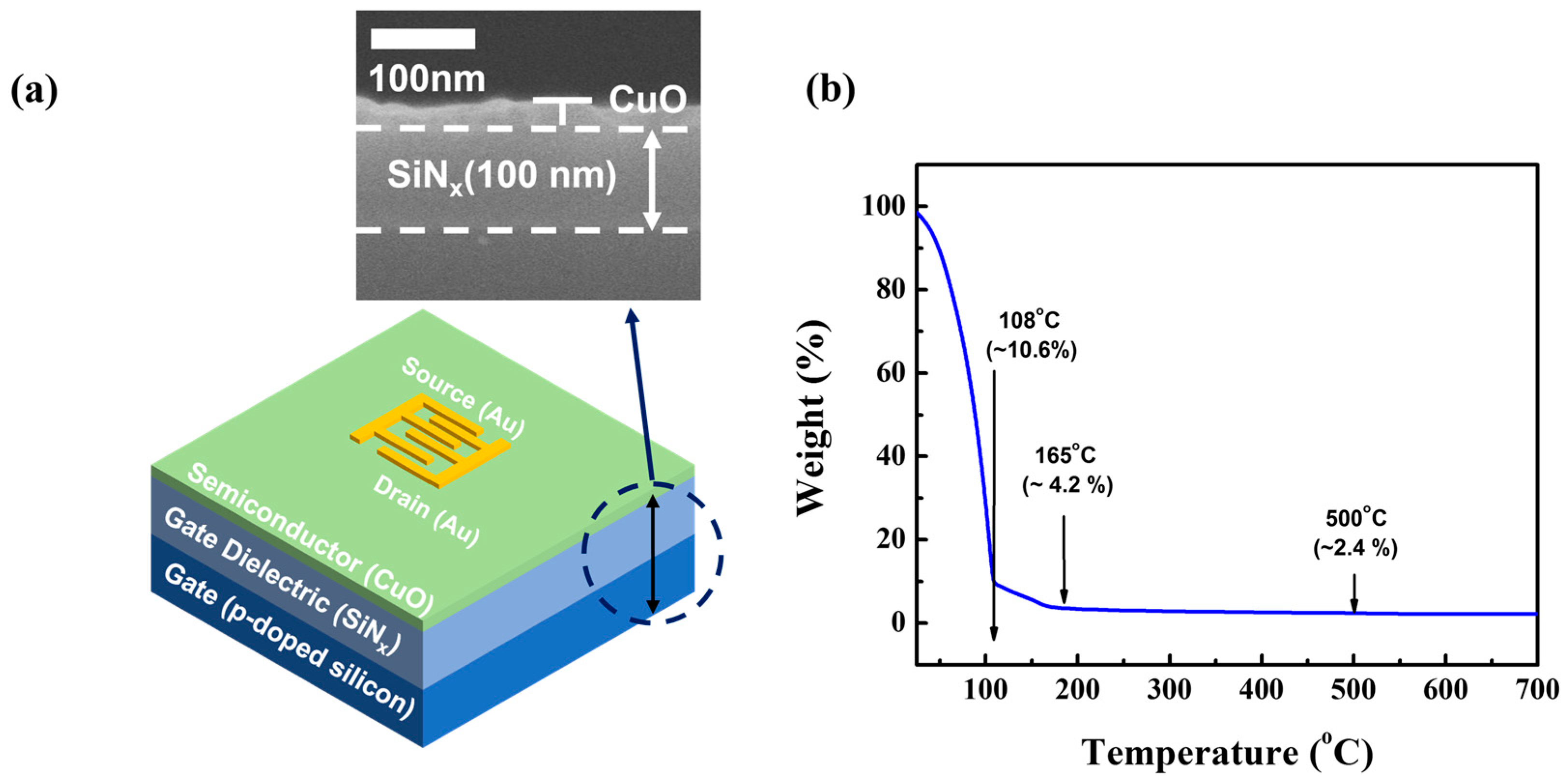
2. Materials and Methods
3. Results and Discussion
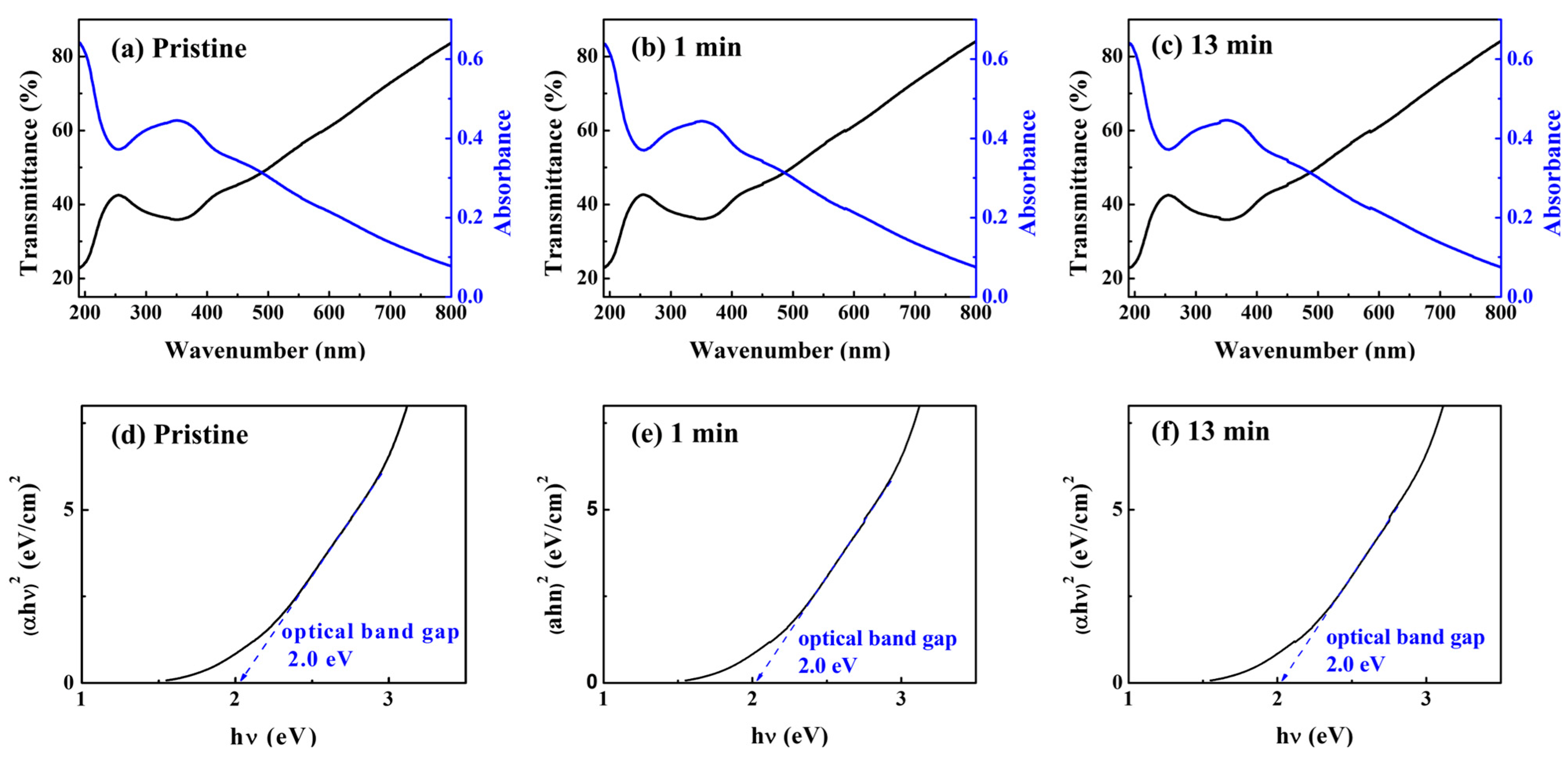
3.1. Optical Characteristics
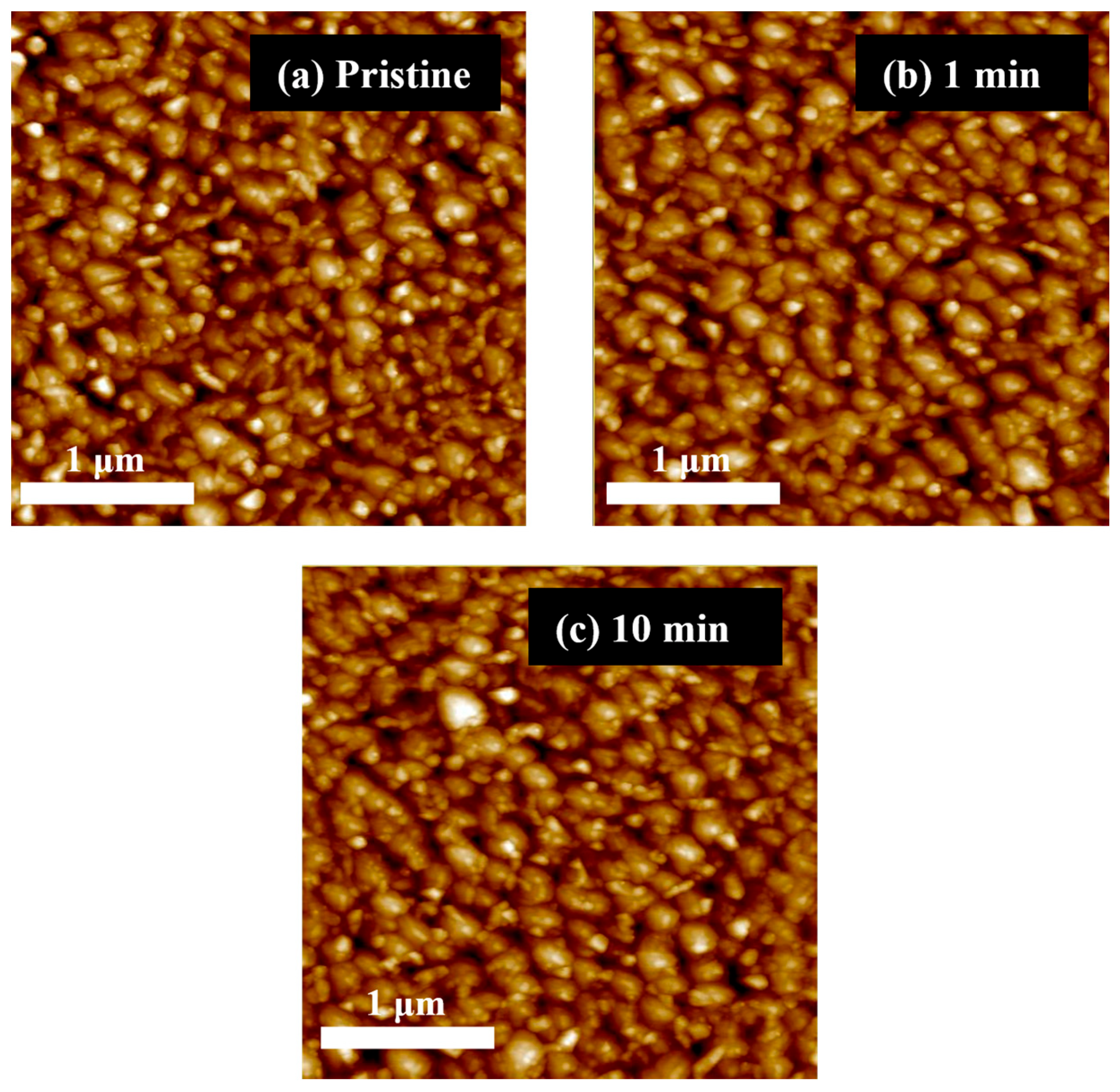
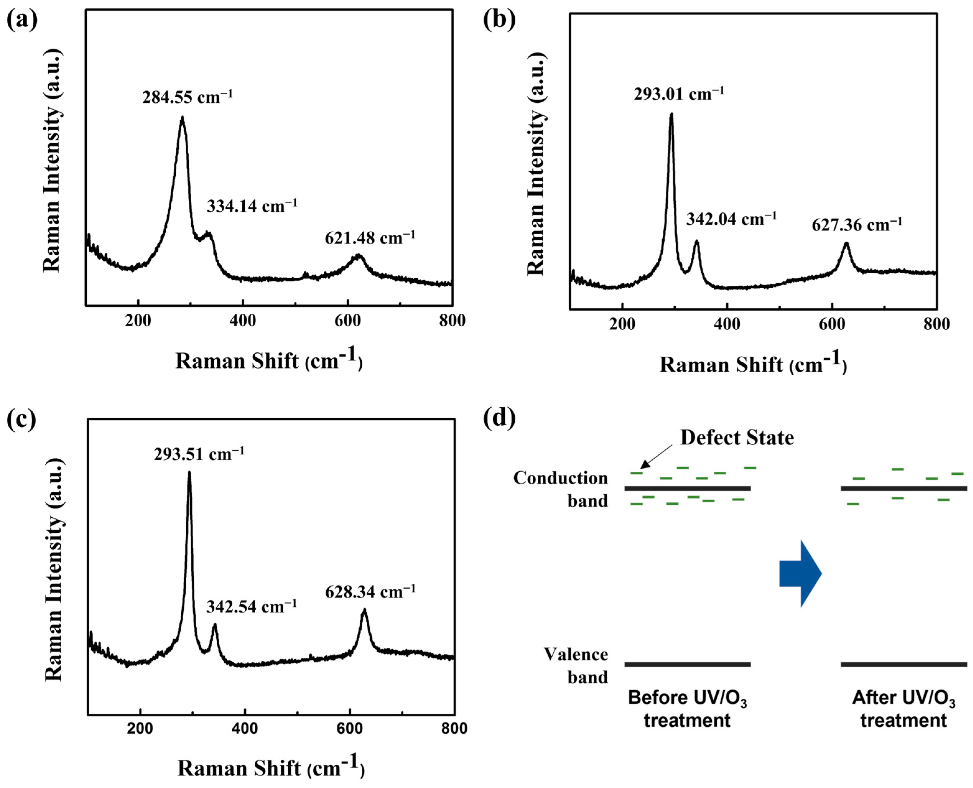
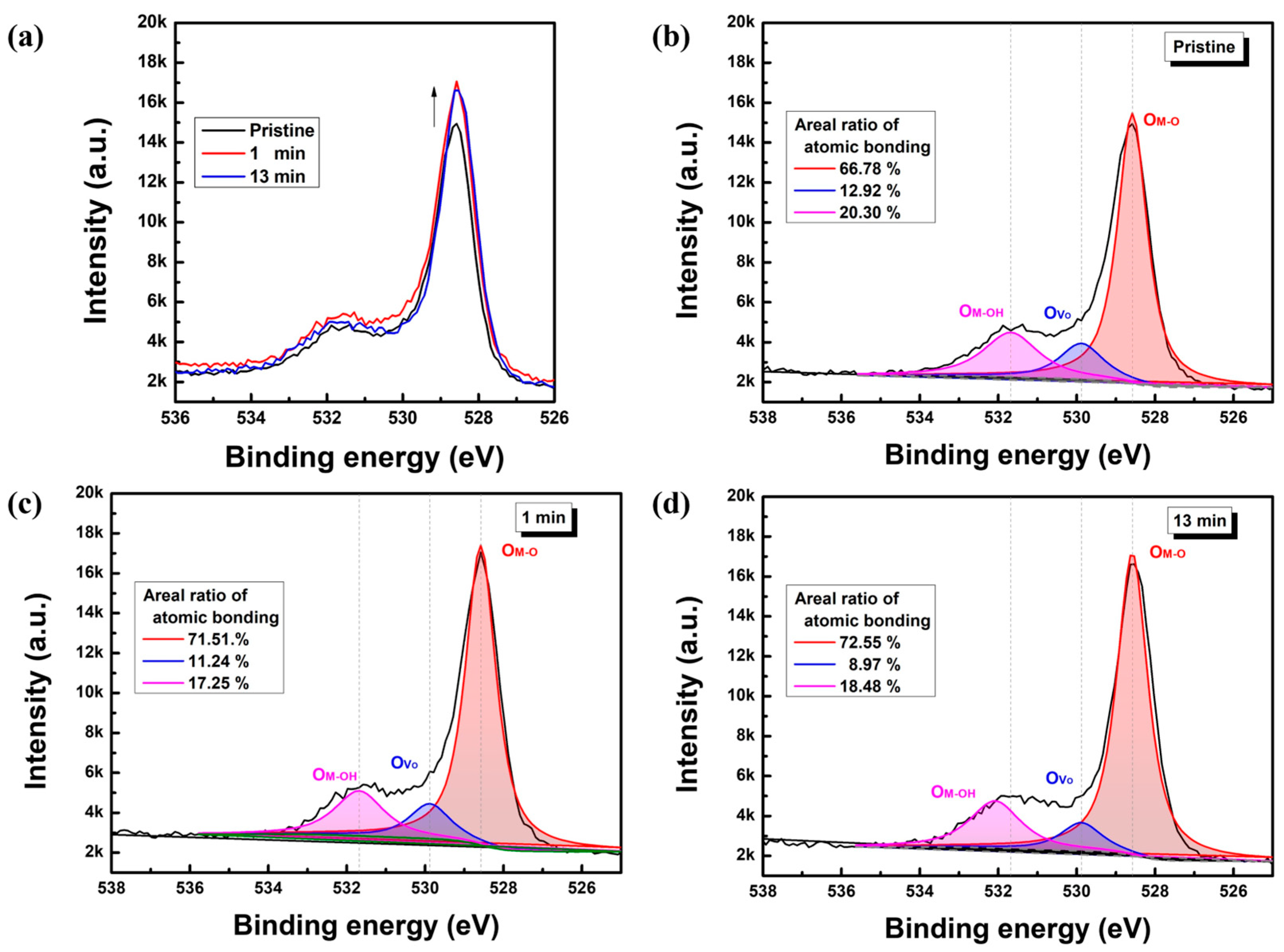
3.2. Structural and Stoichiometric Characteristics
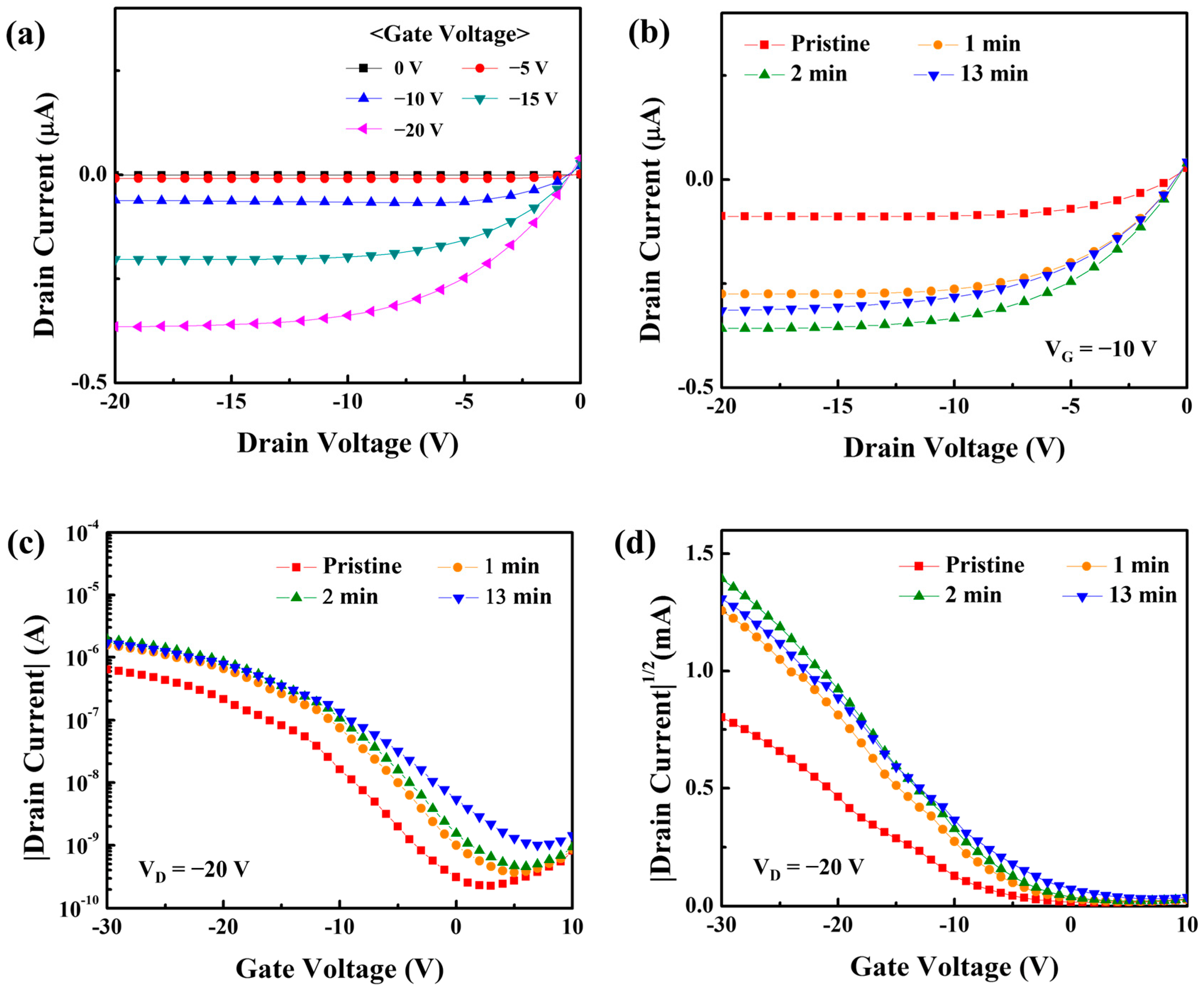
3.3. Electrical Characteristics
4. Conclusions
Author Contributions
Funding
Institutional Review Board Statement
Informed Consent Statement
Data Availability Statement
Conflicts of Interest
References
- Wang, H.; He, J.; Xu, Y.; André, N.; Zeng, Y.; Flandre, D.; Liao, L.; Li, G. Impact of hydrogen dopant incorporation on InGaZnO, ZnO and In2O3 thin film transistors. Phys. Chem. Chem. Phys. 2020, 22, 1591–1597. [Google Scholar] [CrossRef] [PubMed]
- Kawaharamura, T.; Uchida, T.; Wang, D.; Sanada, M.; Furuta, M. Enhancing carrier mobility of IGZO TFT fabricated by non-vacuum mist CVD with O3 assistance. Phys. Status Solidi 2013, 10, 1565–1568. [Google Scholar] [CrossRef]
- Kang, B.H.; Park, K.; An, J.B.; Kim, H.J. Recent Progress in Oxide Semiconductor Based Thin-Film Transistors for Next-Generation Display. Mater. Matters™ 2021, 1, 3–13. [Google Scholar]
- Zhang, Q.; Xia, G.; Li, L.; Xia, W.; Gong, H.; Wang, S. High-performance Zinc-Tin-Oxide thin film transistors based on environment friendly solution process. Curr. Appl. Phys. 2019, 19, 174–181. [Google Scholar] [CrossRef]
- Ouyang, Z.; Wang, W.; Dai, M.; Zhang, B.; Gong, J.; Li, M.; Qin, L.; Sun, H. Research Progress of p-Type Oxide Thin-Film Transistors. Materials 2022, 15, 4781. [Google Scholar] [CrossRef]
- Magari, Y.; Kataoka, T.; Yeh, W.; Furuta, M. High-mobility hydrogenated polycrystalline In2O3 (In2O3: H) thin-film transistors. Nat. Commun. 2022, 13, 1078. [Google Scholar] [CrossRef]
- Seo, J.S.; Jeon, J.H.; Hwang, Y.H.; Park, H.; Ryu, M.; Park, S.H.K.; Bae, B.S. Solution-processed flexible fluorine-doped indium zinc oxide thin-film transistors fabricated on plastic film at low temperature. Sci. Rep. 2013, 3, 2085. [Google Scholar] [CrossRef] [Green Version]
- Kim, T.; Jeong, J.K. Recent Progress and perspectives of field-effect transistors based on p-type oxide semiconductors. Phys. Status Solidi (RRL)–Rapid Res. Lett. 2022, 16, 2100394. [Google Scholar] [CrossRef]
- Wang, Z.; Nayak, P.K.; Caraveo-Frescas, J.A.; Alshareef, H.N. Recent developments in p-Type oxide semiconductor materials and devices. Adv. Mater. 2016, 28, 3831–3892. [Google Scholar] [CrossRef] [Green Version]
- Lee, H.; Zhang, X.; Kim, E.J.; Park, J. Structural and electrical characteristics of solution-processed copper oxide films for application in thin-film transistors. Sensor. Mater 2019, 31, 501–507. [Google Scholar] [CrossRef]
- Kawazoe, H.; Yasukawa, M.; Hyodo, H.; Kurita, M.; Yanagi, H.; Hosono, H. P-type electrical conduction in transparent thin films of CuAlO2. Nature 1997, 389, 939–942. [Google Scholar] [CrossRef]
- Bae, J.H.; Lee, J.H.; Park, S.P.; Jung, T.S.; Kim, H.J.; Kim, D.; Lee, S.; Park, K.; Yoon, S.; Kang, I.; et al. Gallium doping effects for improving switching performance of p-type copper (I) oxide thin-film transistors. ACS Appl. Mater. Interfaces 2020, 12, 38350–38356. [Google Scholar] [CrossRef]
- Kim, T.; Yoo, B.; Youn, Y.; Lee, M.; Song, A.; Chung, K.B.; Han, S.; Jeong, J.K. Material design of new p-type tin oxyselenide semiconductor through valence band engineering and its device application. ACS Appl. Mater. Interfaces 2019, 11, 40214–40221. [Google Scholar] [CrossRef]
- Zeng, X.; Zhukova, M.; Faniel, S.; Li, G.; Flandre, D. Room-temperature DC-sputtered p-type CuO accumulation-mode thin-film transistors gated by HfO2. Appl. Phys. Lett. 2022, 121, 133503. [Google Scholar] [CrossRef]
- Seo, S.J.; Hwang, Y.H.; Bae, B.S. Postannealing process for low temperature processed sol–gel zinc tin oxide thin film transistors. Electrochem. Solid State Lett. 2010, 13, H357. [Google Scholar] [CrossRef]
- Faber, H.; Hirschmann, J.; Klaumünzer, M.; Braunschweig, B.; Peukert, W.; Halik, M. Impact of oxygen plasma treatment on the device performance of zinc oxide nanoparticle-based thin-film transistors. ACS Appl. Mater. Interfaces 2012, 4, 1693–1696. [Google Scholar] [CrossRef]
- Mane, A.U.; Allen, A.J.; Kanjolia, R.K.; Elam, J.W. Indium oxide thin films by atomic layer deposition using trimethylindium and ozone. J. Phys. Chem. C 2016, 120, 9874–9883. [Google Scholar] [CrossRef]
- Ur Rehman, A.; Aadil, M.; Zulfiqar, S.; Agboola, P.O.; Shakir, I.; Aboud, M.F.A.; Haider, S.; Warsi, M.F. Fabrication of binary metal doped CuO nanocatalyst and their application for the industrial effluents treatment. Ceram. Int. 2021, 47, 5929–5937. [Google Scholar] [CrossRef]
- Bharathi, E.; Sivakumari, G.; Kamalakkannan, J.; Karthikeyan, B.; Senthilvelan, S. Synergetic execute pressure, temperature on mixed Ac/Ag@ CuO and its multi properties of solar light elucidation and antibacterial activity by hydrothermal technique. Mater. Sci. Energy Technol. 2020, 3, 407–419. [Google Scholar] [CrossRef]
- Xu, J.F.; Ji, W.; Shen, Z.X.; Li, W.S.; Tang, S.H.; Ye, X.R.; Jia, D.Z.; Xin, X.Q. Raman spectra of CuO nanocrystals. J. Raman Spectrosc. 1999, 30, 413–415. [Google Scholar] [CrossRef]
- McCarthy, J.; Perova, T.S.; Moore, R.A.; Bhattacharya, S.; Gamble, H.; Armstrong, B.M. Composition and stress analysis in Si structures using micro-raman spectroscopy. Scanning: J. Scanning Microsc. 2004, 26, 235–239. [Google Scholar] [CrossRef] [PubMed]
- Zardo, I.; Conesa-Boj, S.; Peiro, F.; Morante, J.R.; Arbiol, J.; Uccelli, E.; Abstreiter, G.; i Morral, A.F. Raman spectroscopy of wurtzite and zinc-blende GaAs nanowires: Polarization dependence, selection rules, and strain effects. Phys. Rev. B 2009, 80, 245324. [Google Scholar] [CrossRef] [Green Version]
- Jeong, S.; Lee, J.Y.; Lee, S.S.; Seo, Y.H.; Kim, S.Y.; Park, J.U.; Ryu, B.H.; Yang, W.; Moon, J.; Choi, Y. Metal salt-derived In–Ga–Zn–O semiconductors incorporating formamide as a novel co-solvent for producing solution-processed, electrohydrodynamic-jet printed, high performance oxide transistors. J. Mater. Chem. A 2013, 1, 4236–4243. [Google Scholar] [CrossRef] [Green Version]
- Kim, D.W.; Park, J.; Hwang, J.; Kim, H.D.; Ryu, J.H.; Lee, K.B.; Baek, K.H.; Do, L.M.; Choi, J.S. Rapid curing of solution-processed zinc oxide films by pulse-light annealing for thin-film transistor Applications. Electron. Mater. Lett. 2015, 11, 82–87. [Google Scholar] [CrossRef]
- Park, S.C.; Kim, D.; Shin, H.; Lee, D.K.; Zhang, X.; Park, J.; Choi, J.S. Advanced photo-annealing of indium zinc oxide films for thin-film transistors using pulse UV light. J. Inf. Display. 2016, 17, 1–7. [Google Scholar] [CrossRef] [Green Version]
- Kim, W.; Lee, W.J.; Kwak, T.; Beak, S.; Lee, S.H.; Park, S. Influence of UV/Ozone treatment on threshold voltage modulation in sol-gel IGZO thin-film transistors. Adv. Mater. Interfaces. 2022, 9, 2200032. [Google Scholar] [CrossRef]
- Huang, C.Y.; Xiao, L.K.; Chang, Y.H.; Chen, L.Y.; Chen, G.T.; Li, M.H. High-performance solution-processed ZnSnO metal–semiconductor–metal ultraviolet photodetectors via ultraviolet/ozone photo-annealing. Semicond. Sci. Technol. 2021, 36, 095013. [Google Scholar] [CrossRef]
- Shang, Z.W.; Hsu, H.H.; Zheng, Z.W.; Cheng, C.H. Progress and challenges in p-type oxide-based thin film transistors. Nanotechnol. Rev. 2019, 8, 422–443. [Google Scholar] [CrossRef]
- Chou, C.Y.; Lin, C.H.; Chen, W.H.; Li, B.J.; Liu, C.Y. High-dielectric-constant silicon nitride thin films fabricated by radio frequency sputtering in Ar and Ar/N2 gas mixture. Thin Solid Film. 2020, 709, 138198. [Google Scholar] [CrossRef]


| Bulk Concentration (1015 cm−3) | Hall Mobility (cm2 V−1 s−1) | Conductivity (10−3 Ω−1 cm−1) | |
|---|---|---|---|
| Pristine | 1.05 ± 0.7 | 96.7 ± 39.8 | 4.4 ± 2.9 |
| Post-UV/O3 treatment | 1.10 ± 0.2 | 280 ± 99.3 | 45.7 ± 19.7 |
| UV/Ozone Treatment Period (min) | VT (V) | ION/OFF | μeff (cm2 V−1 s−1) |
|---|---|---|---|
| Pristine | −7.32 | 2.83 × 10³ | 1.81 × 10⁻³ |
| 1 | −5.97 | 4.29 × 10³ | 4.38 × 10⁻³ |
| 2 | −5.12 | 4.26 × 10³ | 4.97 × 10⁻³ |
| 13 | −3.76 | 1.69 × 10³ | 3.82 × 10⁻³ |
Disclaimer/Publisher’s Note: The statements, opinions and data contained in all publications are solely those of the individual author(s) and contributor(s) and not of MDPI and/or the editor(s). MDPI and/or the editor(s) disclaim responsibility for any injury to people or property resulting from any ideas, methods, instructions or products referred to in the content. |
© 2023 by the authors. Licensee MDPI, Basel, Switzerland. This article is an open access article distributed under the terms and conditions of the Creative Commons Attribution (CC BY) license (https://creativecommons.org/licenses/by/4.0/).
Share and Cite
Lee, H.; Kim, D.; Shin, H.; Bae, J.-H.; Park, J. Effects of Post-UV/Ozone Treatment on Electrical Characteristics of Solution-Processed Copper Oxide Thin-Film Transistors. Nanomaterials 2023, 13, 854. https://doi.org/10.3390/nano13050854
Lee H, Kim D, Shin H, Bae J-H, Park J. Effects of Post-UV/Ozone Treatment on Electrical Characteristics of Solution-Processed Copper Oxide Thin-Film Transistors. Nanomaterials. 2023; 13(5):854. https://doi.org/10.3390/nano13050854
Chicago/Turabian StyleLee, Hyeonju, Dongwook Kim, Hyunji Shin, Jin-Hyuk Bae, and Jaehoon Park. 2023. "Effects of Post-UV/Ozone Treatment on Electrical Characteristics of Solution-Processed Copper Oxide Thin-Film Transistors" Nanomaterials 13, no. 5: 854. https://doi.org/10.3390/nano13050854
APA StyleLee, H., Kim, D., Shin, H., Bae, J.-H., & Park, J. (2023). Effects of Post-UV/Ozone Treatment on Electrical Characteristics of Solution-Processed Copper Oxide Thin-Film Transistors. Nanomaterials, 13(5), 854. https://doi.org/10.3390/nano13050854