
Realization of High Current Gain for Van der Waals MoS2/WSe2/MoS2 Bipolar Junction Transistor


Abstract
:1. Introduction
2. Materials and Methods
2.1. Materials
2.2. Device Fabrication
2.3. Characterization
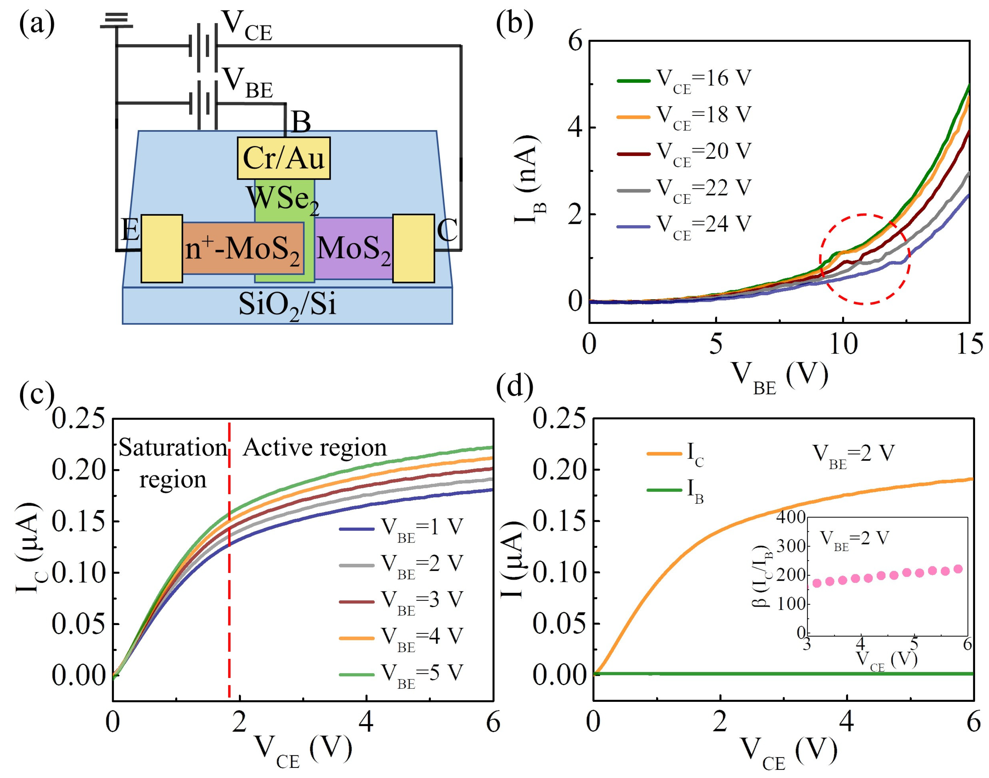
3. Results and Discussion
4. Conclusions
Supplementary Materials
Author Contributions
Funding
Data Availability Statement
Conflicts of Interest
References
- Novoselov, K.S.; Geim, A.K.; Morozov, S.V.; Jiang, D.; Zhang, Y.; Dubonos, S.V.; Grigorieva, I.V.; Firsov, A.A. Electric field effect in atomically thin carbon films. Science 2004, 306, 666–669. [Google Scholar] [CrossRef] [PubMed]
- Chang, C.; Chen, W.; Chen, Y.; Chen, Y.; Chen, Y.; Ding, F.; Fan, C.; Fan Hong, J.; Fan, Z.; Gong, C.; et al. Recent Progress on Two-Dimensional Materials. Acta Phys. Chim. Sin. 2021, 37, 2108017. [Google Scholar] [CrossRef]
- Tan, C.L.; Cao, X.H.; Wu, X.J.; He, Q.Y.; Yang, J.; Zhang, X.; Chen, J.Z.; Zhao, W.; Han, S.K.; Nam, G.H.; et al. Recent Advances in Ultrathin Two-Dimensional Nanomaterials. Chem. Rev. 2017, 117, 6225–6331. [Google Scholar] [CrossRef] [PubMed]
- Zhang, J.; Tan, B.Y.; Zhang, X.; Gao, F.; Hu, Y.X.; Wang, L.F.; Duan, X.M.; Yang, Z.H.; Hu, P. Atomically Thin Hexagonal Boron Nitride and Its Heterostructures. Adv. Mater. 2021, 33, 2000769. [Google Scholar] [CrossRef] [PubMed]
- Bian, R.J.; Li, C.C.; Liu, Q.; Cao, G.M.; Fu, Q.D.; Meng, P.; Zhou, J.D.; Liu, F.C.; Liu, Z. Recent progress in the synthesis of novel two-dimensional van der Waals materials. Natl. Sci. Rev. 2022, 9, nwab164. [Google Scholar] [CrossRef] [PubMed]
- Tian, Y.; Zeng, X.J.; Xing, Y.; Chen, J.; Deng, S.Z.; She, J.C.; Liu, F. High-Performance Planar Field-Emission Photodetector of Monolayer Tungsten Disulfide with Microtips. Small 2023, 19, 2304233. [Google Scholar] [CrossRef] [PubMed]
- Liu, Y.; Weiss, N.O.; Duan, X.D.; Cheng, H.C.; Huang, Y.; Duan, X.F. Van der Waals heterostructures and devices. Nat. Rev. Mater. 2016, 1, 16042. [Google Scholar] [CrossRef]
- Castellanos-Gomez, A.; Duan, X.F.; Fei, Z.; Gutierrez, H.R.; Huang, Y.; Huang, X.Y.; Quereda, J.; Qian, Q.; Sutter, E.; Sutter, P. Van der Waals heterostructures. Nat. Rev. Methods Primers 2022, 2, 58. [Google Scholar] [CrossRef]
- Massicotte, M.; Schmidt, P.; Vialla, F.; Schädler, K.G.; Reserbat-Plantey, A.; Watanabe, K.; Taniguchi, T.; Tielrooij, K.J.; Koppens, F.H.L. Picosecond photoresponse in van der Waals heterostructures. Nat. Nanotechnol. 2016, 11, 42–46. [Google Scholar] [CrossRef]
- Tian, Y.; Guo, Z.; Liu, Z.; Lin, H.; Li, X.; Chen, J.; Deng, S.; Liu, F. Efficiently enhanced the visible-light absorption of monolayer WS2 by constructing an asymmetric Fabry-Perot cavity. Mater. Today Nano 2021, 14, 100112. [Google Scholar] [CrossRef]
- Dastgeer, G.; Nisar, S.; Rasheed, A.; Akbar, K.; Chavan, V.D.; Kim, D.K.; Wabaidur, S.M.; Zulfiqar, M.W.; Eom, J. Atomically engineered, high-speed non-volatile flash memory device exhibiting multibit data storage operations. Nano Energy 2024, 119, 109106. [Google Scholar] [CrossRef]
- Dastgeer, G.; Afzal, A.M.; Aziz, J.; Hussain, S.; Jaffery, S.H.A.; Kim, D.K.; Imran, M.; Assiri, M.A. Flexible Memory Device Composed of Metal-Oxide and Two-Dimensional Material (SnO2/WTe2) Exhibiting Stable Resistive Switching. Materials 2021, 14, 7535. [Google Scholar] [CrossRef] [PubMed]
- Nisar, S.; Basha, B.; Dastgeer, G.; Shahzad, Z.M.; Kim, H.; Rabani, I.; Rasheed, A.; Al-Buriahi, M.S.; Irfan, A.; Eom, J.; et al. A Novel Biosensing Approach: Improving SnS2 FET Sensitivity with a Tailored Supporter Molecule and Custom Substrate. Adv. Sci. 2023, 10, 2303654. [Google Scholar] [CrossRef] [PubMed]
- Kim, Y.; Lee, S.; Song, J.G.; Ko, K.Y.; Woo, W.J.; Lee, S.W.; Park, M.; Lee, H.; Lee, Z.; Choi, H.; et al. 2D Transition Metal Dichalcogenide Heterostructures for p- and n-Type Photovoltaic Self-Powered Gas Sensor. Adv. Funct. Mater. 2020, 30, 2003360. [Google Scholar] [CrossRef]
- He, C.L.; Tang, J.; Shang, D.S.; Tang, J.S.; Xi, Y.; Wang, S.P.; Li, N.; Zhang, Q.T.; Lu, J.K.; Wei, Z.; et al. Artificial Synapse Based on van der Waals Heterostructures with Tunable Synaptic Functions for Neuromorphic Computing. ACS Appl. Mater. Interfaces 2020, 12, 11945–11954. [Google Scholar] [CrossRef]
- Su, B.W.; Zhang, X.L.; Yao, B.W.; Guo, H.W.; Li, D.K.; Chen, X.D.; Liu, Z.B.; Tian, J.G. Laser Writable Multifunctional van der Waals Heterostructures. Small 2020, 16, 2003593. [Google Scholar] [CrossRef] [PubMed]
- Liu, L.W.; Xu, N.S.; Ke, Y.L.; Chen, H.J.; Zhang, Y.; Deng, S.Z. Sensing by Surface Work Function Modulation: High Performance Gas Sensing using van der Waals Stacked Bipolar Junction Transistor. Sens. Actuators B Chem. 2021, 345, 130340. [Google Scholar] [CrossRef]
- Lee, G.; Pearton, S.J.; Ren, F.; Kim, J. Two-Dimensionally Layered p-Black Phosphorus/n-MoS2/p-Black Phosphorus Heterojunctions. ACS Appl. Mater. Interfaces 2018, 10, 10347–10352. [Google Scholar] [CrossRef] [PubMed]
- Su, B.W.; Yao, B.W.; Zhang, X.L.; Huang, K.X.; Li, D.K.; Guo, H.W.; Li, X.K.; Chen, X.D.; Liu, Z.B.; Tian, J.G. A gate-tunable symmetric bipolar junction transistor fabricated via femtosecond laser processing. Nanoscale Adv. 2020, 2, 1733–1740. [Google Scholar] [CrossRef] [PubMed]
- Li, H.; Ye, L.; Xu, J.B. High-Performance Broadband Floating-Base Bipolar Phototransistor Based on WSe2/BP/MoS2 Heterostructure. ACS Photonics 2017, 4, 823–829. [Google Scholar] [CrossRef]
- Luo, Z.T.; Yang, M.M.; Wu, D.S.; Huang, Z.H.; Gao, W.; Zhang, M.L.; Zhou, Y.C.; Zhao, Y.; Zheng, Z.Q.; Li, J.B. Rational Design of WSe2/WS2/WSe2 Dual Junction Phototransistor Incorporating High Responsivity and Detectivity. Small Methods 2022, 6, 2200583. [Google Scholar] [CrossRef] [PubMed]
- Dastgeer, G.; Shahzad, Z.M.; Chae, H.; Kim, Y.H.; Ko, B.M.; Eom, J. Bipolar Junction Transistor Exhibiting Excellent Output Characteristics with a Prompt Response against the Selective Protein. Adv. Funct. Mater. 2022, 32, 2204781. [Google Scholar] [CrossRef]
- Shahidul Hassan, M.M.; Domingos, H. Breakdown voltages of base-collector junctions of medium- and low-voltage graded collector transistors. Int. J. Electron. 1991, 70, 69–75. [Google Scholar] [CrossRef]
- Yuan, J.S. Collector-base junction capacitance of advanced bipolar transistors operating at avalanche breakdown. Phys. Status Solidi A 1992, 134, 575–581. [Google Scholar] [CrossRef]
- Maity, S.; Sarkar, K.; Kumar, P. Layered Heterostructures Based on MoS2/MoSe2 Nanosheets Deposited on GaN Substrates for Photodetector Applications. ACS Appl. Nano Mater. 2023, 6, 4224–4235. [Google Scholar] [CrossRef]
- Zhao, W.J.; Ghorannevis, Z.; Amara, K.K.; Pang, J.R.; Toh, M.; Zhang, X.; Kloc, C.; Tan, P.H.; Eda, G. Lattice dynamics in mono- and few-layer sheets of WS2 and WSe2. Nanoscale 2013, 5, 9677–9683. [Google Scholar] [CrossRef] [PubMed]
- Xiao, J.W.; Zhang, Y.; Chen, H.J.; Xu, N.S.; Deng, S.Z. Enhanced Performance of a Monolayer MoS2/WSe2 Heterojunction as a Photoelectrochemical Cathode. Nano-Micro Lett. 2018, 10, 60. [Google Scholar] [CrossRef] [PubMed]
- Kim, J.; Cho, K.; Pak, J.; Lee, W.; Seo, J.; Kim, J.K.; Shin, J.; Jang, J.; Baek, K.Y.; Lee, J.; et al. Channel-Length-Modulated Avalanche Multiplication in Ambipolar WSe2 Field-Effect Transistors. ACS Nano 2022, 16, 5376–5383. [Google Scholar] [CrossRef]
- Luo, P.; Wang, F.K.; Qu, J.Y.; Liu, K.L.; Hu, X.Z.; Liu, K.W.; Zhai, T.Y. Self-Driven WSe2/Bi2O2Se Van der Waals Heterostructure Photodetectors with High Light On/Off Ratio and Fast Response. Adv. Funct. Mater. 2021, 31, 2008351. [Google Scholar] [CrossRef]
- Zhu, J.Q.; Yue, X.F.; Chen, J.J.; Wang, J.; Wan, J.; Bao, W.Z.; Hu, L.G.; Liu, R.; Cong, C.X.; Qiu, Z.J. Ultrasensitive Phototransistor Based on Laser-Induced P-Type Doped WSe2/MoS2 Van der Waals Heterojunction. Appl. Sci. 2023, 13, 6024. [Google Scholar] [CrossRef]
- Nourbakhsh, A.; Zubair, A.; Dresselhaus, M.S.; Palacios, T. Transport Properties of a MoS2/WSe2 Heterojunction Transistor and Its Potential for Application. Nano Lett. 2016, 16, 1359–1366. [Google Scholar] [CrossRef] [PubMed]
- Yan, X.; Zhang, D.W.; Liu, C.S.; Bao, W.Z.; Wang, S.Y.; Ding, S.J.; Zheng, G.F.; Zhou, P. High Performance Amplifier Element Realization via MoS2/GaTe Heterostructures. Adv. Sci. 2018, 5, 1700830. [Google Scholar] [CrossRef] [PubMed]
- Lin, C.Y.; Zhu, X.D.; Tsai, S.H.; Tsai, S.P.; Lei, S.D.; Shi, Y.M.; Li, L.J.; Huang, S.J.; Wu, W.F.; Yeh, W.K.; et al. Atomic-Monolayer Two-Dimensional Lateral Quasi-Heterojunction Bipolar Transistors with Resonant Tunneling Phenomenon. ACS Nano 2017, 11, 11015–11023. [Google Scholar] [CrossRef] [PubMed]
- Liu, L.W.; Xu, N.S.; Zhang, Y.; Zhao, P.; Chen, H.J.; Deng, S.Z. Van der Waals Bipolar Junction Transistor Using Vertically Stacked Two-Dimensional Atomic Crystals. Adv. Funct. Mater. 2019, 29, 1807893. [Google Scholar] [CrossRef]
- Afzal, A.M.; Iqbal, M.Z.; Dastgeer, G.; Nazir, G.; Mumtaz, S.; Usman, M.; Eom, J. WS2/GeSe/WS2 Bipolar Transistor-Based Chemical Sensor with Fast Response and Recovery Times. ACS Appl. Mater. Interfaces 2020, 12, 39524–39532. [Google Scholar] [CrossRef] [PubMed]
- Son, B.; Wang, Y.D.; Luo, M.L.; Lu, K.Z.; Kim, Y.; Joo, H.J.; Yi, Y.; Wang, C.W.; Wang, Q.J.; Chae, S.H.; et al. Efficient Avalanche Photodiodes with a WSe2/MoS2 Heterostructure via Two-Photon Absorption. Nano Lett. 2022, 22, 9516–9522. [Google Scholar] [CrossRef] [PubMed]
- Ouyang, T.H.; Wang, X.M.; Liu, S.J.; Chen, H.J.; Deng, S.Z. A Complete Two-Dimensional Avalanche Photodiode Based on MoTe2-WS2-MoTe2 Heterojunctions with Ultralow Dark Current. Front. Mater. 2021, 8, 736180. [Google Scholar] [CrossRef]
- Pak, J.; Jang, Y.; Byun, J.; Cho, K.; Kim, T.Y.; Kim, J.K.; Choi, B.Y.; Shin, J.; Hong, Y.; Chung, S.; et al. Two-Dimensional Thickness-Dependent Avalanche Breakdown Phenomena in MoS2 Field-Effect Transistors under High Electric Fields. ACS Nano 2018, 12, 7109–7116. [Google Scholar] [CrossRef] [PubMed]
- Lan, C.Y.; Li, C.; Wang, S.; He, T.Y.; Jiao, T.P.; Wei, D.P.; Jing, W.K.; Li, L.Y.; Liu, Y. Zener Tunneling and Photoresponse of a WS2/Si van der Waals Heterojunction. ACS Appl. Mater. Interfaces 2016, 8, 18375–18382. [Google Scholar] [CrossRef] [PubMed]
- Dastgeer, G.; Khan, M.F.; Nazir, G.; Afzal, A.M.; Aftab, S.; Naqvi, B.A.; Cha, J.; Min, K.A.; Jami, Y.; Jung, J.; et al. Temperature-Dependent and Gate-Tunable Rectification in a Black Phosphorus/WS2 van der Waals Heterojunction Diode. ACS Appl. Mater. Interfaces 2018, 10, 13150–13157. [Google Scholar] [CrossRef] [PubMed]


| Material | Structure | Type | α | β | Ref. |
|---|---|---|---|---|---|
| n+-MoS2/WSe2/MoS2 | Vertical | npn | 0.98 | 225 | This work |
| MoTe2/GeSe/MoTe2 | Vertical | npn | 0.95 | 29.3 | [22] |
| MoS2/WSe2/MoS2 | Vertical | npn | 0.97 | 12 | [34] |
| WS2/GeSe/WS2 | Vertical | npn | 1.11 | 20.7 | [35] |
| MoS2/WSe2/MoS2 | Lateral | npn | / | 3 | [33] |
| MoS2/BP/MoS2 | Lateral | npn | 0.98 | 41 | [16] |
Disclaimer/Publisher’s Note: The statements, opinions and data contained in all publications are solely those of the individual author(s) and contributor(s) and not of MDPI and/or the editor(s). MDPI and/or the editor(s) disclaim responsibility for any injury to people or property resulting from any ideas, methods, instructions or products referred to in the content. |
© 2024 by the authors. Licensee MDPI, Basel, Switzerland. This article is an open access article distributed under the terms and conditions of the Creative Commons Attribution (CC BY) license (https://creativecommons.org/licenses/by/4.0/).
Share and Cite
Yan, Z.; Xu, N.; Deng, S. Realization of High Current Gain for Van der Waals MoS2/WSe2/MoS2 Bipolar Junction Transistor. Nanomaterials 2024, 14, 718. https://doi.org/10.3390/nano14080718
Yan Z, Xu N, Deng S. Realization of High Current Gain for Van der Waals MoS2/WSe2/MoS2 Bipolar Junction Transistor. Nanomaterials. 2024; 14(8):718. https://doi.org/10.3390/nano14080718
Chicago/Turabian StyleYan, Zezhang, Ningsheng Xu, and Shaozhi Deng. 2024. "Realization of High Current Gain for Van der Waals MoS2/WSe2/MoS2 Bipolar Junction Transistor" Nanomaterials 14, no. 8: 718. https://doi.org/10.3390/nano14080718
APA StyleYan, Z., Xu, N., & Deng, S. (2024). Realization of High Current Gain for Van der Waals MoS2/WSe2/MoS2 Bipolar Junction Transistor. Nanomaterials, 14(8), 718. https://doi.org/10.3390/nano14080718