1. Introduction
Nowadays, with stringent size restrictions and integration requirements for MMICs, a great number of MMICs, such as limiters and switches, adopt balanced and unbalanced test pad structures in layout design, like GS (Ground Signal) pad or SG pad, to replace large-size balanced pads such as GSG pad. These chips require both balanced and unbalanced RF probes for on-wafer testing. Due to the differences of transmission modals of electromagnetic fields, traditional on-wafer thru standards based on single balanced or unbalanced structure adopt different structural dimensions to match the characteristic impedances of corresponding RF probes. However, traditional thru standards cannot meet the impedance matching requirements of hybrid balanced and unbalanced RF probes at the same time, resulting in a sharp decrease in calibration accuracy. In the research of widely used calibration methods, such as SOLT (Short Open Load Thru), TRL (Thru Reflect Line), and LRRM (Line Reflect-Reflect Match), researchers have presented several solutions [
1,
2,
3,
4,
5,
6,
7] to improve the on-wafer calibration and measurement. However, traditional thru standards are unavoidable in these calibration methods, which poses a severe challenge for on-wafer testing based on hybrid balanced and unbalanced probes.
A MMIC test based on hybrid balanced and unbalanced RF probes belongs to heteromorphy structure tests, the S-parameter of which cannot be directly measured by traditional calibration method. For heteromorphy structures, two main kinds of solutions have been proposed by researchers. One is to remove the insertion loss of the RF probes and other adapters by scalar calculation based on the direct compensation method. However, this method does not include vector error correction and, thus, cannot be applied to high-frequency and high-precision test due to the lack of accuracy. The other is to use the OSL second-order de-embedding method [
8] to obtain the S-parameters of the RF probes and other adapters with high accuracy, and then achieve the S-parameters of the heteromorphy structure by vector error correction and de-embedding [
9,
10,
11,
12] But the measurement accuracy of this method is quite sensitive to errors between the ideal calibration plane and the actual calibration plane.
In this paper, after evaluating the calibration error of MMIC tests with hybrid balanced and unbalanced RF probes based on the traditional SOLR calibration technique [
13,
14,
15,
16,
17], an MMIC on-wafer test method based on balanced and unbalanced RF pad structure is proposed. This method combines an OSL second-order de-embedding technique with vector error correction, and cascade matrix transformation technique, which introduces the vector error correction to the actual calibration plane and further improves the accuracy of the S-parameter extraction of the RF probe. After the vector error correction and de-embedding, the calibration reference plane can be accurately transferred to the probe tips, as a result, significantly improving the test accuracy. Besides, an automatic test system is built with the aid of the C# object-oriented language [
18], which realizes the automatic performance of instrument control, data acquisition, result correction, data analysis, and graphical presentation of the results.
The rest of this paper is divided into four sections: The first section evaluates the calibration error of the traditional test method, the second section introduces on-wafer test method of heteromorphy structure based on hybrid balanced and unbalanced RF probes in detail, the third section analyzes and verifies the approach based on the test results, and the last section draws the conclusion.
2. The Calibration Error Evaluation of Traditional Test Method
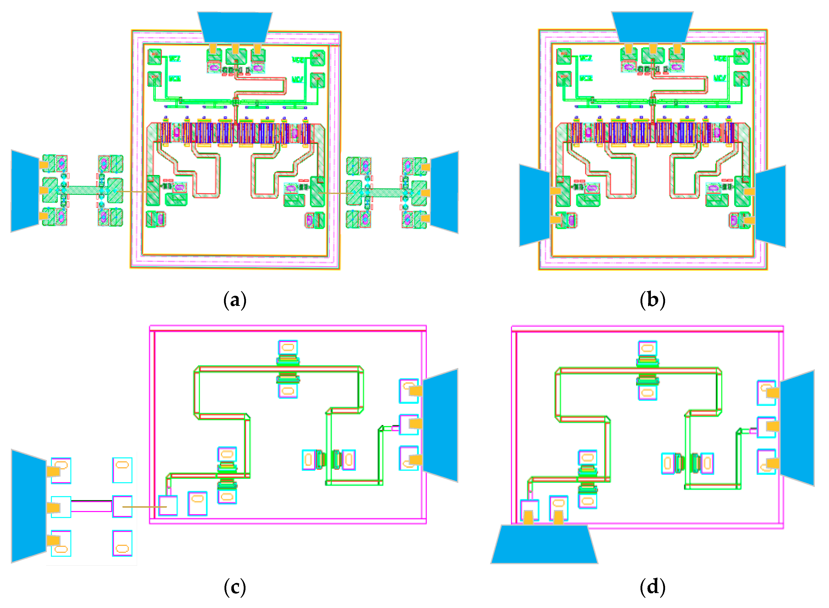
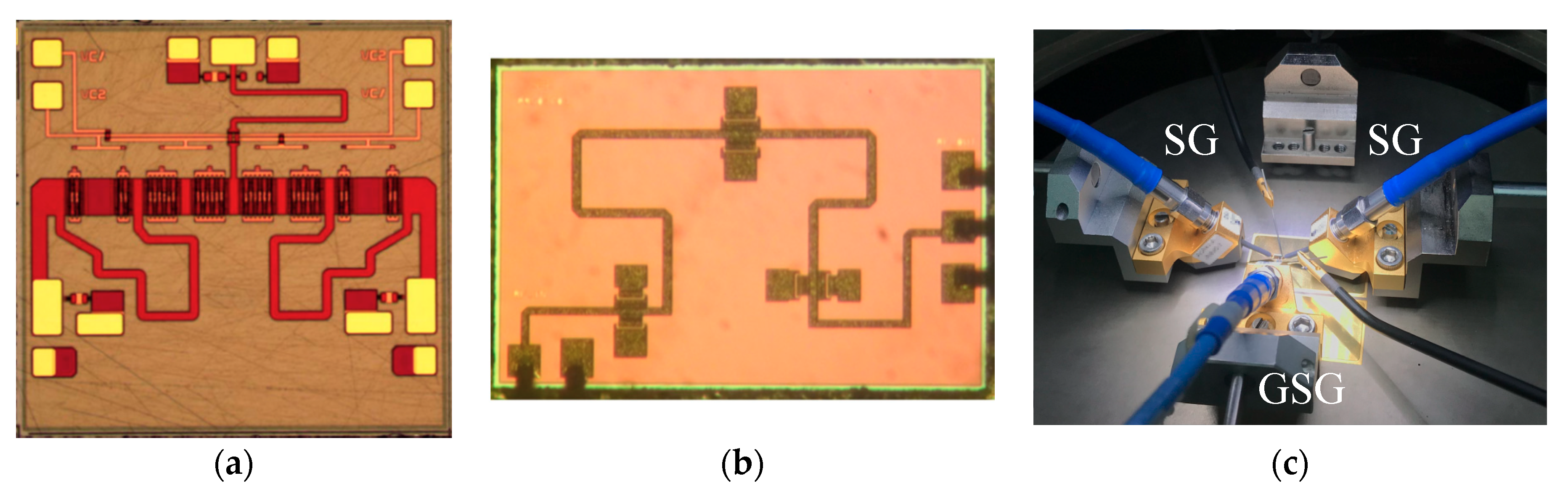
More and more MMICs adopt balanced and unbalanced test pad structures in layout design due to the stringent size restrictions and integration requirements. For this kind of heteromorphy structures, the calibration error of two traditional test methods are evaluated. The SPDT switch chip and limiter chip with both GSG and SG pads shown in
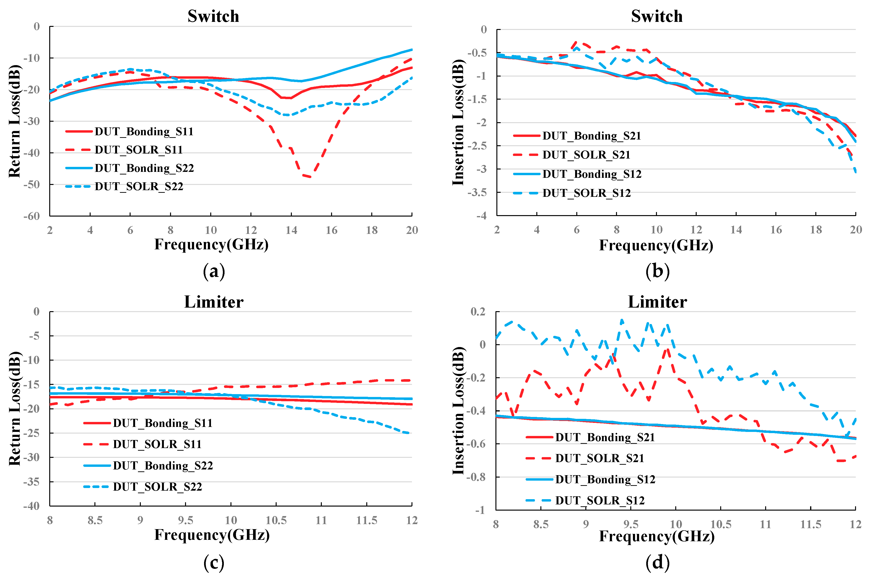
Figure 1 are used as an example. The bottoms of both chips are metalized. The first method turns each unbalanced SG pad into a conventional GSG pad by wire bonding to a GSG through structure, so that the structure of balanced GSG pads at both ends can be calibrated with classic method. Then, the S-parameters of the chips are obtained by S-parameter de-embedding of the GSG through structure together with the bonding wire from the measured results. The results of the “wire-bonding” method are highly consistent with the real values, and are thus used as references in this paper. However, after the test, the micro-assembly of the chips cannot be fully recovered without damage. Thus, this method can only be applied to evaluation tests but not to large-scale on-wafer test. The second method directly adopts SOLR for heteromorphy structure on-wafer calibration by ignoring the calibration error. The comparison between the test results of these two methods is shown in
Figure 2. Although the “direct SOLR” method does not destroy the chip, it cannot be applied due to the large result deviation.
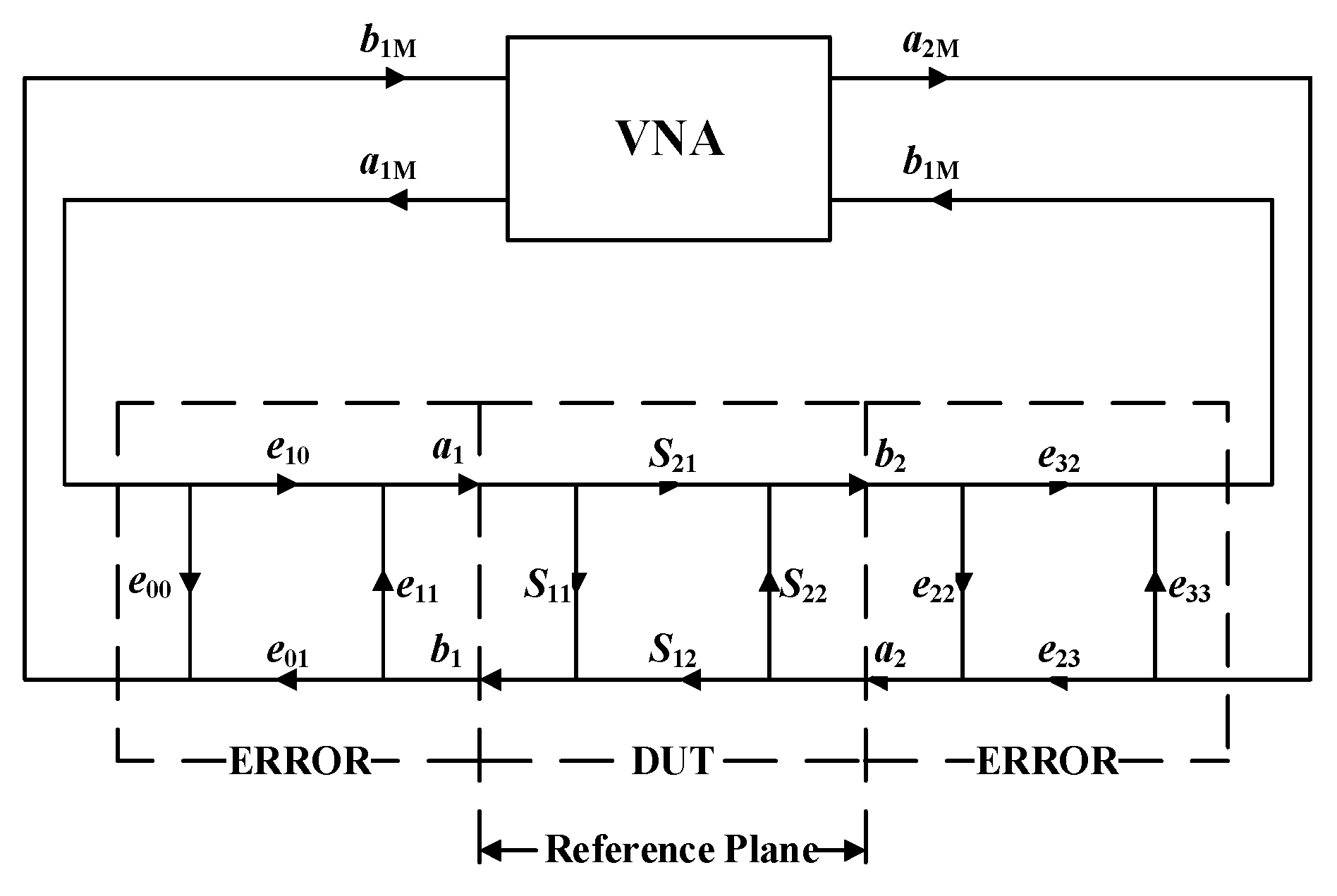
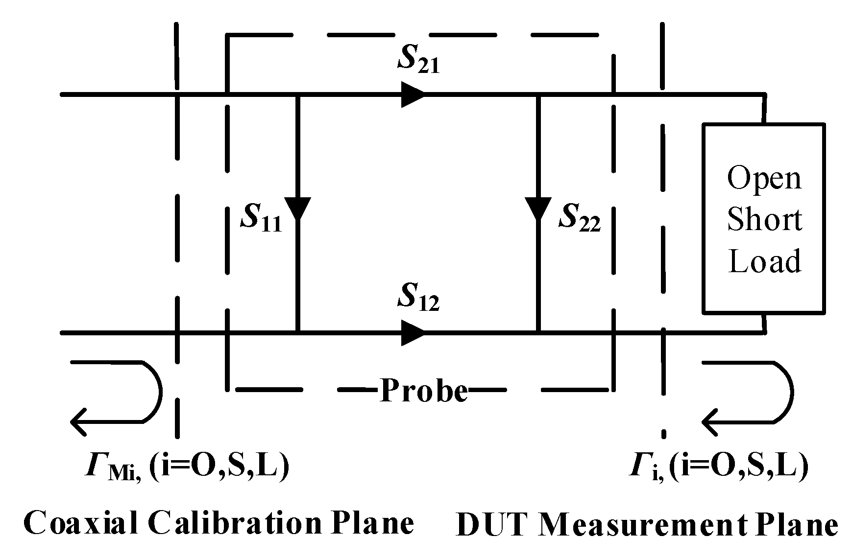
Further reasons of the failure of the second test method are as follows. The signal flow graph of the eight-error terms model used in the SOLR calibration method is shown in
Figure 3. VNA (Vector Network Analyzer, Keysight, CA, USA) is adopted for testing. The transmission matrix between the VNA transceiver’s plane and the MMIC plane is represented by a two-port error matrix [
19,
20,
21]. The product error equations related to thru calibration is shown in Equations (1) and (2).
Among them, EDF (forward directivity error), EDR (reverse directivity error), ESF (forward source mismatch error), ESR (reverse source mismatch error), ERF (forward reflection tracking error), ERR (reverse reflection tracking error) can be obtained by the calibration of Open, Short and Load standards. Other error terms, ELF (forward load mismatch error), ELR (reverse load mismatch error), ETF (forward transmission tracking error), and ETR (reverse transmission tracking error) require the test of thru standard. As shown in Equations (3)–(6), represents the S-parameter of thru standard. For this kind of passive and reciprocal device, there is , and the EXF (forward crosstalk error) and EXR (reverse crosstalk error) can be ignored.
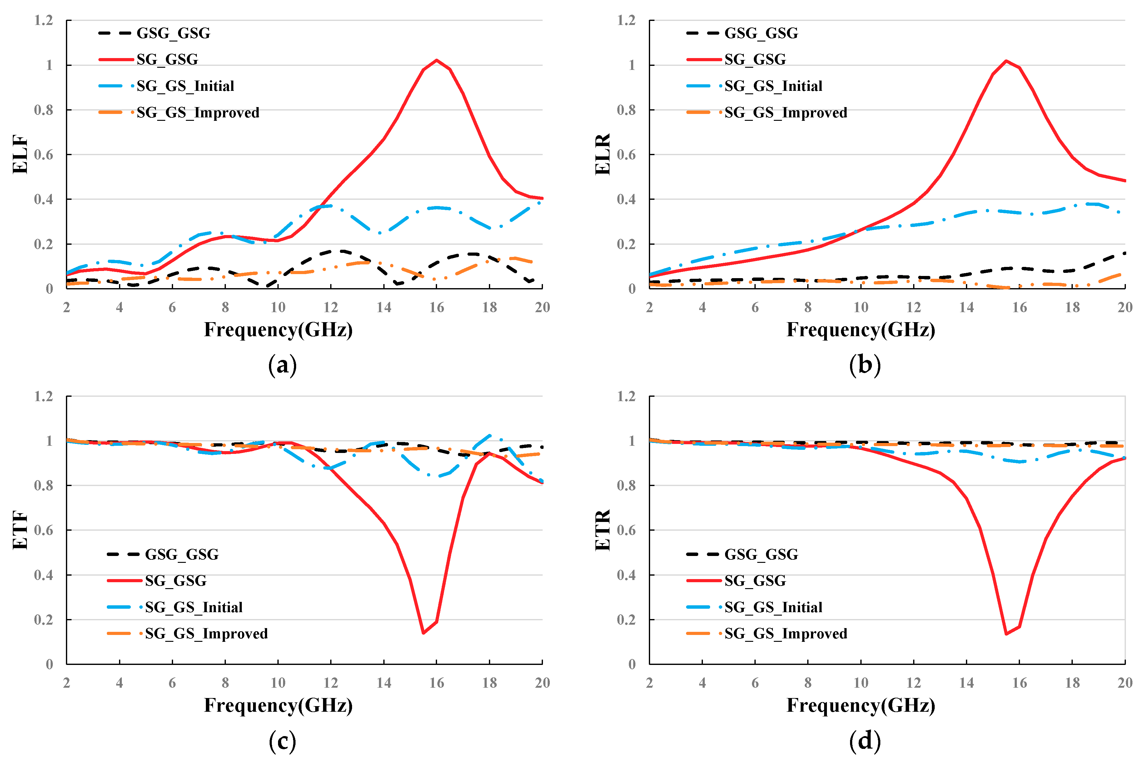
For the tests with different types of probes, full-wave electromagnetic simulations are performed to obtain the S-parameters of the corresponding thru structures shown in
Figure 4 and
Figure 5, referring to the right angle ISS (Impedance Standard Substrate) for up to 67 GHz provided by Cascade (Substrate Material: Alumina; Thickness: 625 μm ± 25 μm; Dielectric constant: 9.9). Then, after substituting the S-parameters of the thru structures into the error model Equations (3)–(6), the error terms are obtained. As shown in
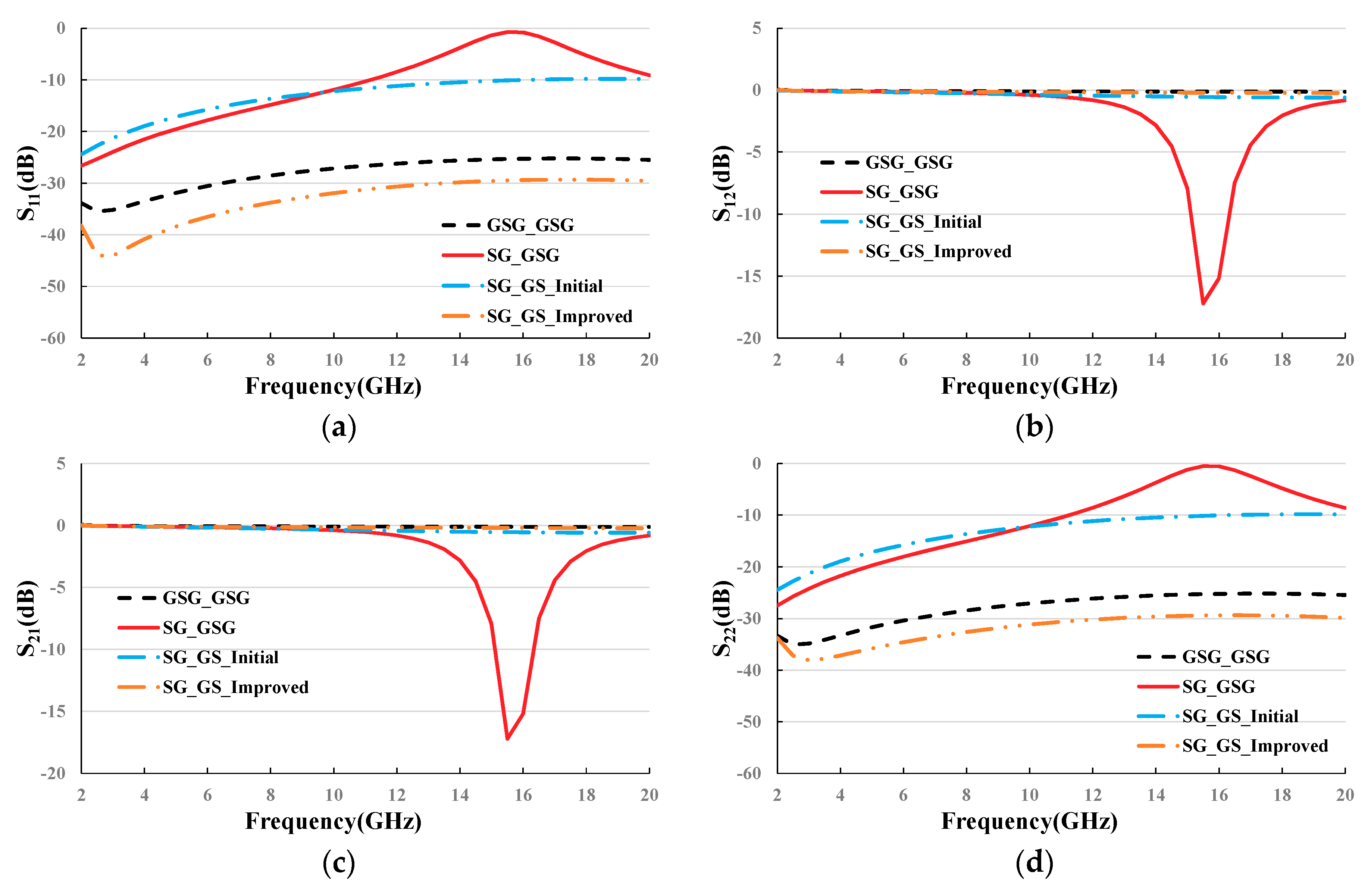
Figure 6, when using the SG-GSG probes (
Figure 4b) or SG-GS probes (
Figure 4c) for SOLR calibration, the port impedance mismatch have a significant impact on the error model parameters, causing large deviation in the test results of MMICs [
22]. Moreover, in order to meet the port matching conditions, the gap between S and G should be modified when using the SG-GS probes for SOLR calibration, as shown in
Figure 4d, but there is no corresponding ISS. Therefore, the traditional GSG thru standard cannot meet the SG port matching requirements and the correct ELF, ELR, ETR, and ETF error model parameters cannot be obtained. As a result, the errors of product terms
and
derived from them are further enlarged, resulting in unreliable test results shown in
Figure 2.
From above, it can be known that the traditional on-wafer thru standard based on balanced structure cannot meet the impedance matching requirements of the hybrid balanced and unbalanced RF probes at the same time. Therefore, the calibration accuracy is greatly reduced. In the following section, a new solution which can be applied for wafer-scale test with good accuracy is presented.
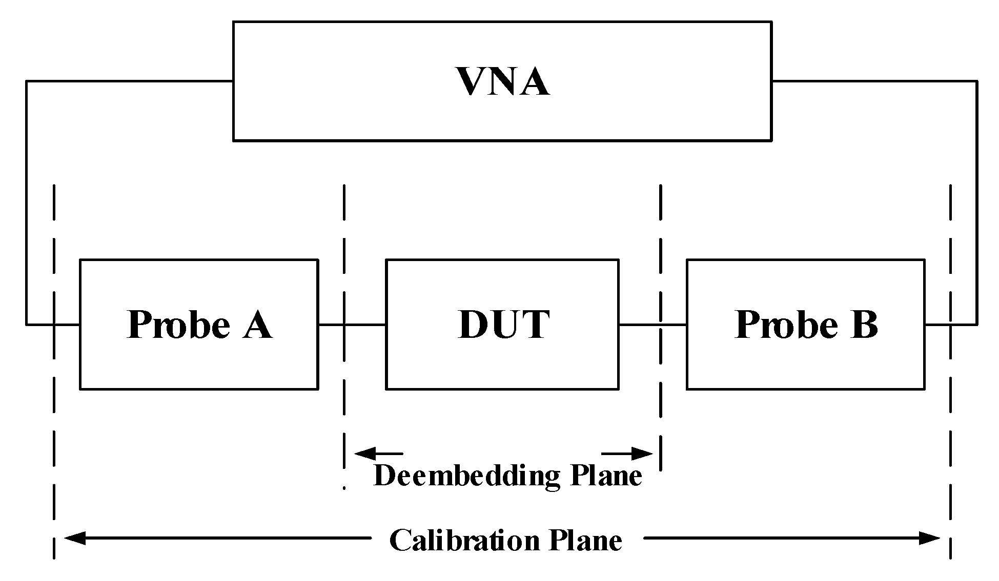
3. On-Wafer Test Method of Heteromorphy Structure
In order to solve the accuracy issues of the existing test methods, this paper proposes an on-wafer test approach of MMIC based on hybrid balanced and unbalanced RF probes by combining OSL second-order de-embedding technique with vector error correction and cascade matrix transformation technique. With the aid of vector error correction, the calibration reference plane is accurately extended to the probe tip surface.
The signal flow graph of OSL second-order de-embedding is shown in
Figure 7. Firstly, the coaxial calibration is performed; then the Open, Short and Load standards, with known reflection coefficients
, are measured to obtain the reflection coefficient
at the coaxial calibration plane. Assuming that the Load calibration matches well (
), the S-parameters of the RF probes can be obtained according to Equations (7) and (8). Generally, the three-order polynomial models of the capacitance and the inductance are used to characterize the Open, Short and Load standards, and their reflection coefficients
,
and
can be obtained with the help of Equations (9) and (10).
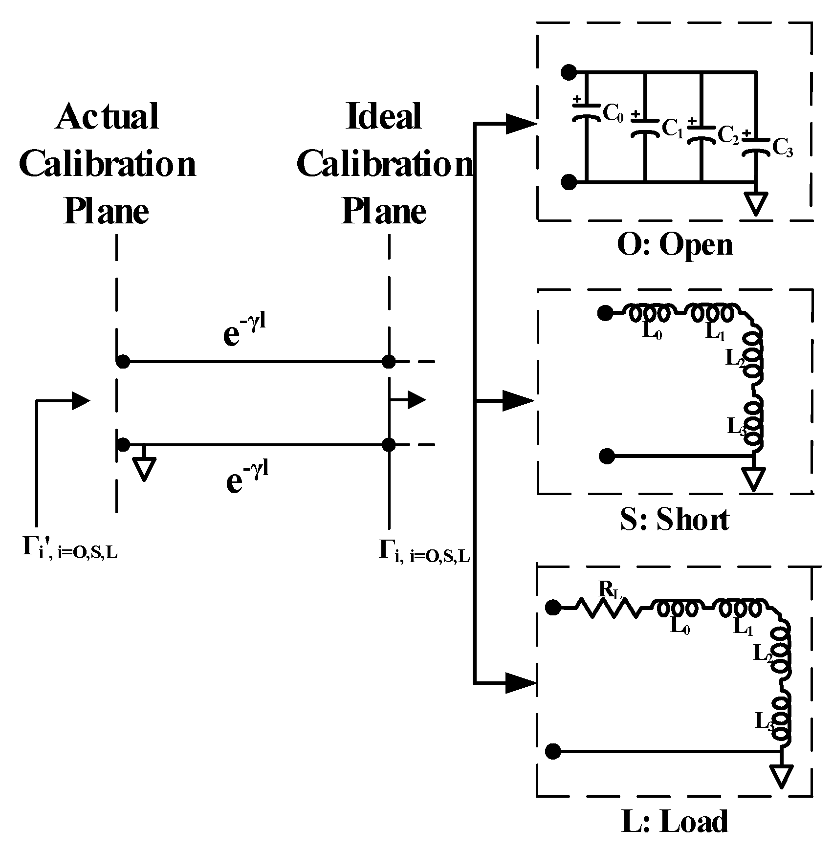
Actually, there are certain deviations between the ideal calibration plane and the actual calibration plane (physical contact) of the non-ideal standards due to the existence of the transmission line. The attenuation and phase shift introduced by the deviation can be described by an equivalent transmission line model. And the transmission line correction algorithm is further used to eliminate these deviations by Equations (11)–(14). The simplified equivalent model is shown in
Figure 8, where
represents the reflection coefficient of the ideal standard,
is the actual coefficient after correction, and
is the correction factor. α and β are the attenuation constant and phase constant of the transmission line, offset_loss and offset_delay are the insertion loss and time delay of the transmission line, generally provided by the ISS manufacturer [
23]. Function
is the curve fitting factor, and offset_Z
0 is the characteristic impedance of the transmission line with a typical value of 50 Ω.
After substituting
into Equation (8), the corrected two-port S-parameters of the RF probes can be extracted. The RF probes are passive reciprocal devices, whose S-parameters meet the formula
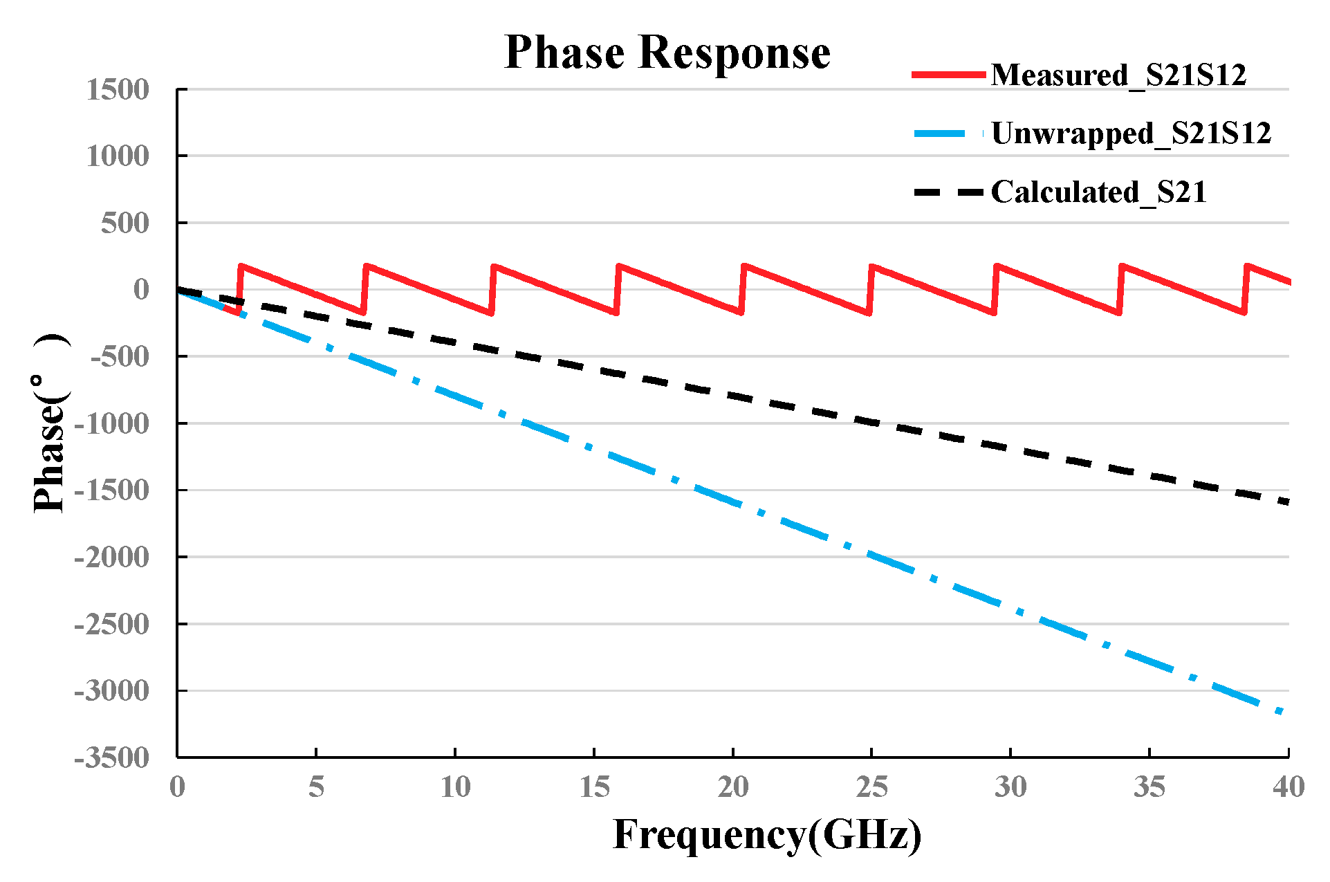
, resulting in phase uncertainty problem [
24]. To solve this problem, phase continuity and supplementary condition
are introduced to select the phase branch, as shown in
Figure 9. The true phase-frequency response of
both before and after the square root should be continuous and the phase at zero frequency point is zero degree. First, the initial folded phase response of
(red solid line) is unfolded (blue dot-dash line) based on the principle of phase continuity. Afterwards, a 180° cycle extension is performed along the vertical axis and a branch (blue dot-dash line) with a zero-frequency phase of 0° is selected, and the phase frequency response of the phase branch is divided by 2 to obtain a true phase frequency response (black dash line).
After obtaining the S-parameters (
,
) of the balanced and unbalanced RF probes, the overall S-parameter of the MMIC at coaxial calibration plane (
), including the hybrid balanced and unbalanced RF probes, is measured. Then, the cascade matrix transformation technique is used to obtain the S-parameter of the MMIC (
) by probe parameters (
,
) de-embedding from the test result (
). The block diagram of the test system is shown in
Figure 10.
The scattering parameter matrixes
,
and
are transformed into the transmission parameter matrixes
,
and
by using Equation (15), where
,
,
and
meet Equation (16). Then the inverse matrix operation is performed, and the transmission parameter matrix
of the DUT is obtained according to Equation (17). Finally, the transmission parameter
of the DUT is converted into desired scattering parameter
according to Equation (18).
4. Test Results and Analysis
Based on the on-wafer test method of the heteromorphy structure proposed in
Section 3, this paper designed an on-wafer test system shown in
Figure 11 to validate the solution. The system consists of a vector network analyzer (Keysight PNA N5224A), GSG and SG RF probes (Cascade ACP-A-GSG-150, ACP-A-SG-150) and a microwave probe station (Cascaded Summit 11000BS). The switch and limiter chips mentioned in
Figure 1 are selected as test samples. The photos of the MMICs are shown in
Figure 11a,b, and the photo of the on-wafer test system based on the hybrid GSG-SG RF probes is shown in
Figure 11c.
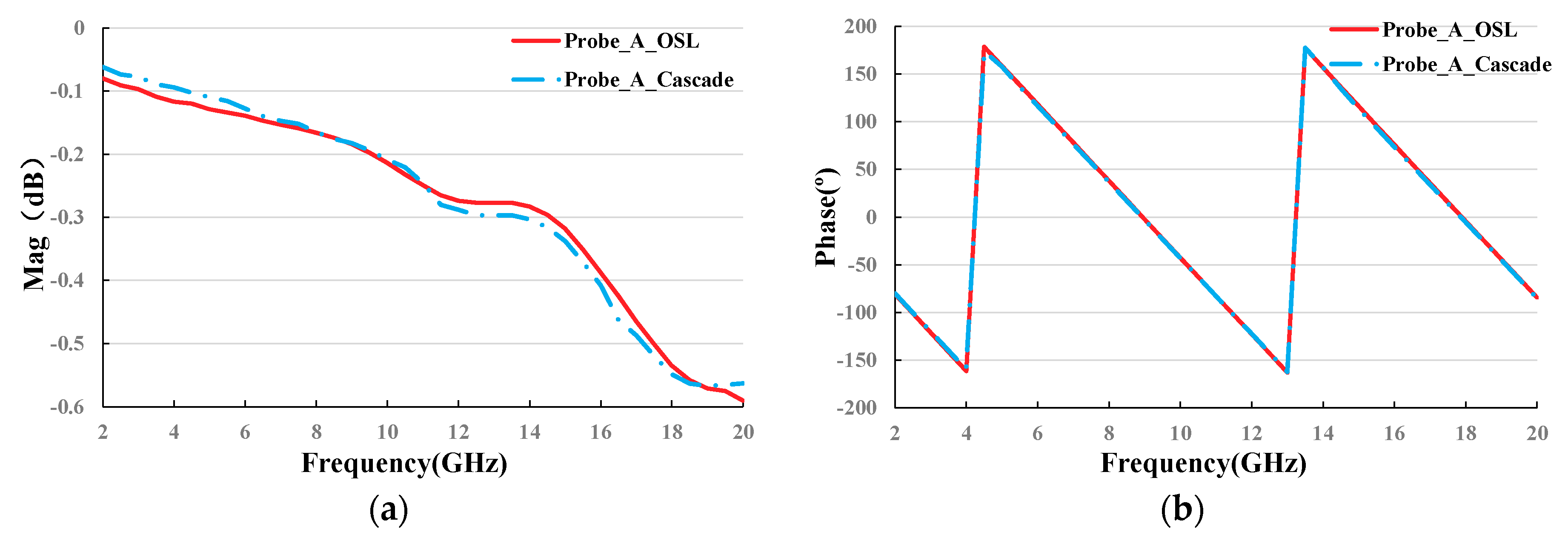
The S-parameters of the SG and GSG probes obtained from the presented OSL method with vector error correction are compared with the parameters provided by Cascade. It can be seen from
Figure 12 that the data obtained from the presented method is basically the same with factory data.
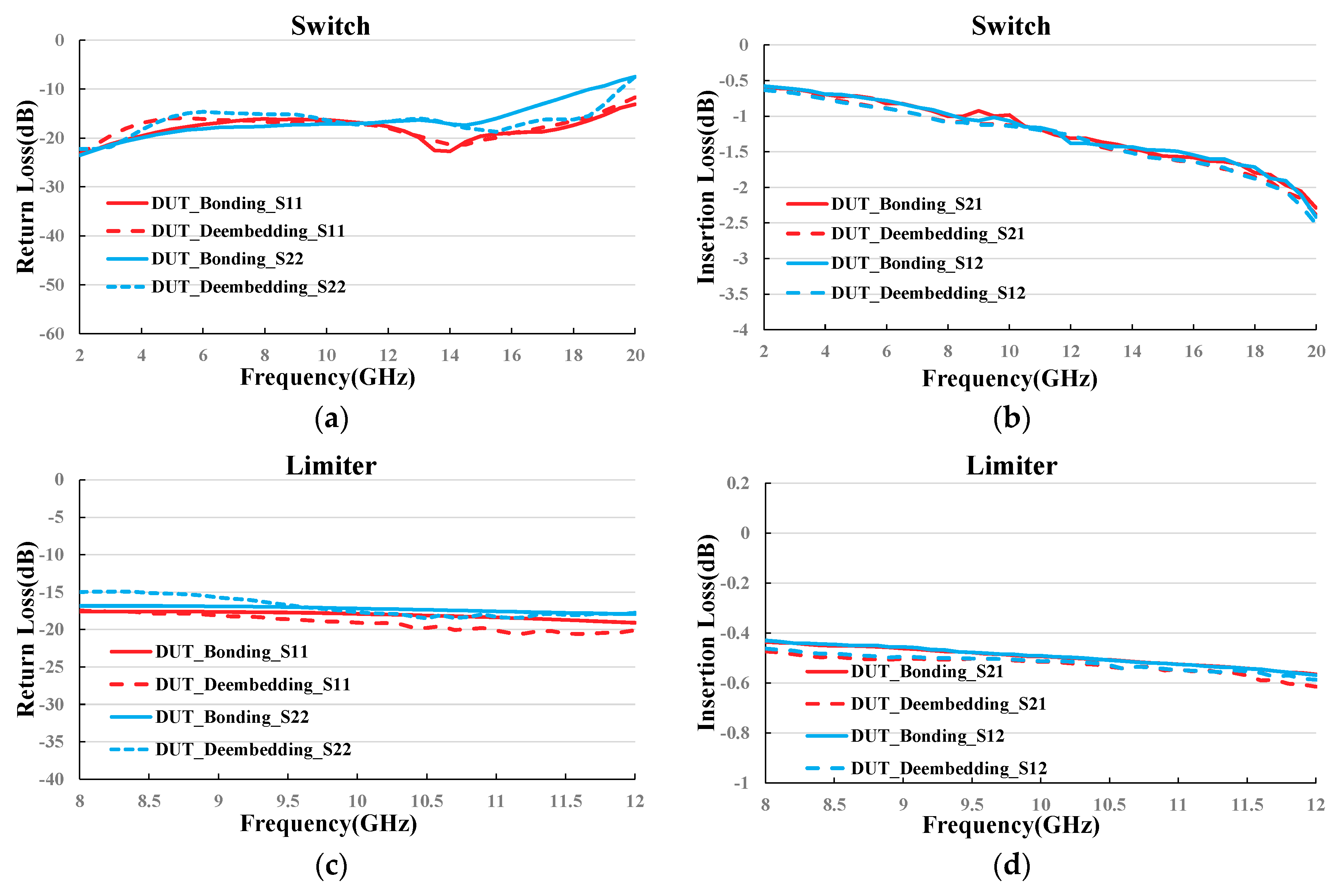
The S-parameters comparison between the test results of the method proposed in this paper and the test results of the “wire-bonding” method mentioned in
Section 2 is shown in
Figure 13. It can be seen that the two results are quite close. The accuracy of our method is highly enhanced comparing with the “direct SOLR” method shown in
Figure 2.
Since the method proposed in this paper requires a large number of complex and matrix operations, object-oriented C# language is used to build an automatic test program. The results interface of the test program is shown in
Figure 14. The program can execute a fully automatic operation covering instrument control, data acquisition, results correction, data analysis and display of graphical results, which avoids human interference, and solves the test efficiency problems faced with the wafer-scale test.


