Article

Micrometric Growth Defects of DLC Thin Films

1
IRCER, UMR CNRS 7315, Université de Limoges, 87068 Limoges, France
2
Oerlikon Balzers Coating France, 87068 Limoges, France
3
Laboratoire ICB, UMR CNRS 6303, Université Bourgogne Franche Comté, 21078 Dijon, France
4
Oerlikon Balzers Coating Germany GmbH, 51427 Bergisch Gladbach, Germany
*
Author to whom correspondence should be addressed.
Current address: IRCER, Centre Européen de la Céramique, 12 Rue Atlantis, 87068 Limoges, France.
Submission received: 7 October 2019 / Revised: 30 October 2019 / Accepted: 2 November 2019 / Published: 14 November 2019
(This article belongs to the Special Issue Characterization of Disorder in Carbons)

Abstract

:
Defects in diamond-like carbon coatings deposited on corrosion sensitive 100Cr6 steel have been studied. Diamond-like carbon (DLC) thin films are promising for corrosion protection due to chemical inertness and low electrical conductivity. Nevertheless, the performance of these coating is highly sensitive to the presence of uncoated areas. These defects represent the primary way of substrate degradation in aggressive environments. An in situ optical microscopy coupled to an electrochemical activation was developed to reveal micrometric growth defects and observe that they were at the origin of corrosion. A square wave voltammetry was applied to increase the sensitivity of electrochemical techniques based on the detection of the dissolution of the bare metal surface triggered by the presence of uncoated spots. This method can be utilized to quantify defect density arising from vapor deposition processes.

Graphical Abstract

1. Introduction

Diamond-like carbon (DLC) is a family of amorphous thin films materials consisting of a disordered network of carbon atoms with a mixture of both sp3 and sp2 bonds [1]. The carbon sp3 hybridization leads to high hardness and low wear rate while the sp2 hybridization results in low friction. The combination of these properties are highly desirable for many engineering applications involving tribological contacts between solid surfaces. DLC have been intensively investigated in the last decades [2,3,4,5]. DLC also present a high chemical inertness, and high electrical resistivity, and a very dense amorphous microstructure. This combination of properties opens the possibilities for its use in applications for the protection of metal against corrosion.
DLC films need sublayers to accommodate stresses when employed in mechanical applications, but it is possible to coat metallic substrates directly with DLC just to evaluate its corrosion protection performance. In some studies, various metallic substrates from carbon steel to stainless steel through other alloys have been coated with 650 nm to 1.5 μm of DLC with plasma assisted chemical vapor deposition (PACVD) technique and tested using standard electrochemical tests (like polarization test, electrochemical impedance spectroscopy (EIS), etc.) in various solutions based on the environment where coated parts will be subjected to [6,7,8,9,10,11]. The main conclusion is that DLC acts as a physical barrier against electrolyte contact with substrates. However, currents in cathodic and anodic domains are measured on coated samples despite the insulating characteristic of DLC material. The authors agree on the origin of this recorded current that must be due to defects in the DLC layers. Some even refer to porosity [12,13]. However, none of these studies presented detailed observations or characterizations of these defects like their sizes, distribution, or their genesis. Kim et al. have tried to quantify these defects or porosities using polarization curves via polarization resistance, corrosion potential, and current determinations [14]. In addition, the determination of pore resistance in the EIS technique using the equivalent circuit for describing the AC (Alternative Current) response of a defective non-conducting polymer film on a metallic substrate is employed to estimate porosity of DLC coatings [12,13,15]. These approaches are questionable because they are not correlated with direct observations of uncoated areas or porosities. Moreover, during the corrosion through porosity or uncoated spots, the metal surface exposed to the electrolyte is expanding and invalidate a hypothesis for their calculation.
Corrosion protection by DLC coatings including ceramic hard sublayers has not been studied a lot as it is difficult to separate the contribution of each individual layer. However, the evaluation of corrosion protection of hard ceramic on sensitive material have been largely studied by Fenker et al. and Panjan et al. in exhaustive papers [16,17,18]. They also conclude on the predominant role of growth defects in the corrosion failure of parts coated with such layers.
The purpose of this work is, therefore, to investigate the origin of the corrosion of DLC coated steel. To perform that, the study starts on classic electrochemical techniques (polarization curve), and then presents a new innovative technique combining an electrochemical test sequence and in situ observations using a digital microscope. In parallel, some growth defects are observed by a scanning electron microscope (SEM).

2. Materials and Methods

2.1. Material and Coating

100Cr6 (AISI 52100) (A) and 90MnCrV8 (AISI O2) (B) steel were used as base metal. For (A), disk samples, 3 mm thick, were machined from a 50 mm diameter rod. Then, they were first ground and then polished using a water based diamond suspension (12 μm) for 20 min in order to reach an average roughness of 0.05 μm. For (B), dot samples with a diameter of 22 mm were stamped from an electropolished sheet. In terms of microstructure, they both exhibit a tempered martensitic structure with chromium carbides. Prior installation inside the reactor, the samples were cleaned in an industrial ultrasonic water based cleaning line.
Diamond-like carbon (DLC) coating, used in this paper, was made in an industrial reactor by Oerlikon Balzers (Balzers, Liechtenstein) combining PVD (Physical Vapor Deposition) and PACVD (Plasma Assisted Chemical Vapor Deposition) processes. The resulting DLC film is an amorphous hydrogenated carbon a-C:H with a hardness of 25 GPa. Before the deposition of the two sublayers, samples were sputter cleaned in argon plasma. Table 1 details the architecture and composition of the studied DLC coatings.

2.2. Electrochemical Set-Up

For electrochemical tests, a conventional three-electrodes set-up was used with a platinum counter electrode and a saturated calomel electrode (SCE) reference. All potentials are referred to SCE. The measurement of the absolute electrode potential requires the use of a reference system which consists of a non-polarizable electrochemical half-cell called reference electrode (in our case defined as SCE). The SCE has a potential of +0.248 V versus the Standard Hydrogen Electrode (SHE) in standard conditions (thermodynamic definition) [19]. Currents are given instead of current densities as it does not make sense to deal with them because the exposed areas of steel substrate are not known due to arbitrary defects distribution for DLC coated samples. An AMETEK VersaSTAT 3 potentiostat/galvanostat (Berwyn, PA, USA) was used for the measurements. The electrolyte solution was an aerated 0.1 M NaCl (Analar Normpur analytical reagent VWR BDH Prolabo (Radnor, PA, USA) at pH 6.5 and room temperature.

2.3. Digital Microscope Set-Up for In Situ Observations

In situ observation using digital microscope KEYENCE VHX-5000 (Osaka, Japan) (equipped with long range zoom lens) was coupled to the conventional electrochemical set-up presented before. The set-up is schematically illustrated in Figure 1. The exposed sample area is scalable with a PTFE (Polytetrafluoroethylene also known as Teflon) adhesive mask to measure the electrochemical response of a very localized area.

2.4. SEM-FIB Apparatus

To complete the in situ electrochemical test, the morphology of the coatings before and after corrosion tests were examined with a scanning electron microscope (SEM) ZEISS Crossbeam 550 (Oberkochen, Germany). A field ions beam (FIB) gun integrated in this SEM was used to perform nano-milling and cross-sectional views. A well-controlled thickness of material was removed from the specimen surface by sputtering. A Ga+ beam was employed at 30 kV and 15 nA to mill the sample. Then, to obtain a smooth and well-polished cross section, the final milling step was performed at 30 kV and 700 pA. An energy-dispersive X-rays (EDX) analysis microprobe (Oxford instruments, Abingdon-on-Thames, United Kingdom) was also coupled to SEM to carry out the chemical analysis of these cross sections. They were performed with a 5 kV electron beam.

3. Results and Discussion

3.1. Classic Polarization Experiment

A coated disk surface (100Cr6 coated with DLC coating) of a 12 mm diameter is chosen without any specific features. This surface is the maximum diameter that can be exposed into the electrochemical cell. However, because the surface is too large to be observed at the same time, a reconstructed image, done by VHX software (VHX-5000 series, Keyence, Osaka, Japan) and based on about 20 detailed images, is realized before and after the experiment (Figure 2a,b). The idea is to cover the largest surface and to obtain a maximum of information about corrosion. The polarization applied here was −1 V to +1 V104ogarithm scale representation allows for clearly defining the mixed corrosion potentials. Below this corrosion potential is the cathodic domain where dioxygen and then dihydrogen reduction happens and above it is the anodic domain where dissolution of steel occurs. For both samples, this corrosion potential is around −0.5 V and −0.4 V, indicating that substrate metal is in contact with electrolytes. Regarding curves of uncoated and coated samples in Figure 3, it can be deduced that DLC acts as barrier against electrolyte as the current is three orders of magnitude lower in the cathodic domain for the coated sample. Regarding the anodic domain, the recorded current, for the DLC coated specimen, is quite significant at 1 V even though it is lower than the uncoated one.
Regarding the entire surface (12 mm diameter disk) before and after, corrosion spots have appeared after the polarization (Figure 2). Blue lines are drawn on surfaces following polishing lines and helping to match images. Red rings mark corrosion spots found at the surface. In this case, they are not randomly distributed at the surface but concentrated in one third of it. In addition, they exhibit a round shape but with various sizes.
If a magnified zone from the previous image containing one of these corrosion spots is observed and compared with the same magnified “before” zone, it is nearly impossible to see the starting point of the corrosion spot at this exact location and for this level of magnification (Figure 4a,b).

3.2. Observation of the Coated Surface

A fine observation of DLC coated substrate by digital microscope at higher magnifications has revealed that the surface contains several defects. These defects seem to be a micro-zone with the absence of coating. They measure around 60 to 10 μm. Figure 5 presents three photographs of these uncoated areas of the surface.
The surface has also been observed and studied with an SEM. Figure 6 presents some SEM surface and cross section images of these defects. An EDX analysis performed on the defect bottom (Figure 6a) showed that it was clearly steel surface. This means that the steel substrate, in this area, is clearly exposed to the corrosive environment. In addition, sometimes the formation of nodular or cone type defects is observed (Figure 6b). This nodule has poor adhesion compared to the overall coating and can be removed with mechanical solicitation. Figure 6b presents an example of nodule defects; one of them is partially removed leaving the substrate naked and unprotected.

3.3. Enhancing the Defects’ Detection and Tracking with a Specific Electrochemical Test

A smaller coated surface, compared to the previous 12 mm diameter disk, is placed inside the in situ electrochemical cell. To achieve this, a Teflon mask reduces the surface from diameter 12 mm (maximum exposed surface) down to 4 mm. This surface (0.125 cm2) is clearly visible at reasonable magnification (×200) on a single image (vs. reconstructed image for 12 mm disk).

3.3.1. Evolution of a Coated Surface Containing Defects during Static −1.2 V and +0.4 V Polarization

In situ observation of the coated surface is started under a polarization test that consists of a −1.2 V static polarization. At this potential, the reduction of the H+ proton produces only dihydrogen gas, which is non-destructive for a steel substrate. This reaction is clearly observable by gas bubbling at the surface. Then, a +0.4 V static polarization is done. During +0.4 V polarization, the anodic dissolution is stimulated. Figure 7 and Figure 8 present the i = f ( t ) curves for, respectively, static cathodic and anodic polarizations with an image taken at t = 0 s and at the end the experiments. Please note that experiments have various durations but always enough to see redox reaction phenomena.
Two “macro” defects are clearly identified from initial in situ observations (red rings in Figure 7a). They measure approximately 30 to 50 μm. An open circuit potential (OCP) measurement is done and the value is stable at − 460 mV giving evidence of steel in contact with the solution. As it is difficult to observe any kind of other defect types than micro-uncoated areas, only these two are defined as clear corrosion pinholes candidates. When the −1.2 V potential is applied, a current is detected and reach a steady state of − 9 μA (Figure 7c). Above one of the defects, a gas bubble starts to form and grows, it remains stuck to the surface probably due to surface tension forces. Surprisingly, the other one has no visible bubble, but this doesn’t mean that no reaction occurs for this defect.
Now, + 0.4 V polarization is applied on the same surface, OCP measurement, done before, remains in the same range of −500 mV. As soon as the potential is applied, a current is detected, but, contrary to the previous negative polarization, no steady state is reached and the current increases drastically by jump steps. At t = 840 s, the current exceeds 150 μA. According to the recorded images, these jump steps are correlated with growth of the corrosion pinhole. In this anodic polarization, the two initially identified defects have reacted and led to corrosion pinholes. No other defects have been detected, proving that the recorded current originates only from these two sites. It can be noticed that, contrary to reduction of H+ proton in dihydrogen, the anodic dissolution has occurred on both initially identified defects, which means that anodic polarization is more sensitive to detect preexisting defects.

3.3.2. Evolution of a Coated Surface Containing One Single Defect during Static −1.2 V and +0.4 V Polarization

Now, an area that exhibits a single defect is isolated and placed into the in situ electrochemical cell. The maximum magnification (×500) is used here and thus the 4 mm disk surface is partially visible. Only the area containing the defect is observed and presented. The complete 4 mm diameter zone has been checked at the end of static polarizations to be sure that only one defect has reacted. The defect has a round shape and measures approximately 20 μm in diameter. In the same way as before, a −1.2 V followed by a +0.4 V polarization is performed, and results are presented the same as before (Figure 9 and Figure 10).
In the cathodic polarization, same observations were made with bubbles formation (not displayed on the final image but observed at intermediary stage) and correlated to a steady state current of −1.2 μA. This indicates that the potentiostat is able to detect a defect with surface of 0.31 mm2 on a surface of 12.6 mm2 (more than 40 times smaller) and visualize consequences of reduction reaction.
In the anodic domain, the same trends are also noted. The defect becomes black as corrosion starts and expands in correlation with jump steps and rapid increase of current flow. After 350 s, an anodic current about 13 μA is recorded.

3.3.3. Alternative Static +0.4 V and −1.2 V Polarization Sequence

A specific potentiostatic polarization sequence has been designed (Figure 11) based on previously shown experiments. This sequence consists of a square wave polarization during which the potential of the working electrode is stepped through a series of forward and reverse pulses from −1.2 V for 1 min to + 0.4 V for 1 min. This sequence was chosen to alternatively stimulate bare metal at the bottom of the small defects in an anodic domain to dissolve steel and in a cathodic domain, at sufficiently low potential, to reduce water (more precisely H+ proton) in dihydrogen allowing for mechanically removing corrosion products by H 2 ( g ) bubbles motion. Before water reduction, at a potential close to the corrosion potential, the dissolved dioxygen reduction occurs first. This sequence can be considered as an enhanced defects detection procedure using corrosion reactions. Anodic dissolution increases the size of corroded zones quickly while dihydrogen bubbling aims at removing corrosion products and surrounding DLC films mechanically in order to clearly enhance to optical detection of corrosion spots.
A first experiment using this electrochemical activation combined with digital microscope observations, a 4 mm diameter disk surface of a mirror-like polished steel B (90MnCrV8) coated with the DLC coating is tested (Figure 12). This surface appears to be free of uncoated areas or any visible coating defects. The use of a mirror-like polished specimen helps to easily detect intrinsic features of the coating. During the test, when the square wave polarization is applied, no current was recorded, and the current plot remains flat at 0 μA (Figure 12c). The observation of the exposed surface along the polarization confirms that no feature is visible to suggest corrosion attacks or anything else. This validates that a-C:H is chemically inert with good insulating properties. Thus, as soon as the steel specimen is fully covered by DLC coating and free of defects from deposition stage, the sensitive steel substrate is completely protected against corrosion.
This same 4 mm diameter disk surface of a mirror-like polished QRS steel (90MnCrV8) is retested, but, this time, a single artificial defect is realized at the surface. This artificial defect is done by making an indentation mark with 25 N of load applied with a Vickers indenter tip. A square mark is visible in Figure 13a,c measuring approximately 20 by 20 μm2. The indenter has reached the substrate (estimated depth: 4 μm) and have created cracks field around letting the electrolyte penetrates until the substrate. The same square wave polarization is then applied (Figure 13d), and a focus is made on a smaller surface containing the artificial defect (Figure 13c,e).
Contrary to the previous experiment (Figure 12c), a current is now recorded. At the beginning, it is not significant in the three first anodic steps, but, in the fourth, it drastically increases to reach at step end a value of 40 μA. In the fifth step, the anodic has a steady state value of 20 μA. The cathodic currents remain quite low at 0.4 μA compared to anodic ones. A bubble has been observed in the cathodic step at t = 450 s. The geometry of the squared artificial defect has also changed to become slightly rounded. The test is no longer continued after 540 s to perform a fine observation of the surface. The specimen zone, where the indentation artificial defect is located, is studied in the SEM-FIB device (Figure 14a). Half of the mark made by the Vickers tip is still visible on the left side of the SEM surface image. The other side has been totally removed, probably by the combined alternative effect of bubbling and steel dissolution.
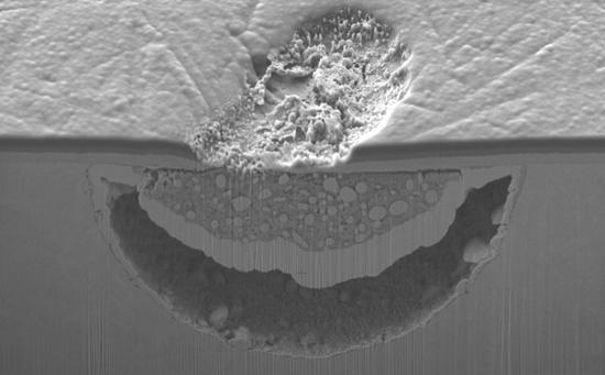
A cross section is performed by FIB milling on half of the defects to observe underneath consequences of the defect on substrate (Figure 14b). The corrosion has propagated along the bended coating and the corroded volume is empty underneath. The gas bubbling as well as the fact that a large part of the coating is removed could be the reason why it is empty.
In addition, finally, on a third sample, an uncoated area found via an SEM observation was isolated. Figure 15a presents an SEM image of this defect untouched before any electrochemical activation. It measures around 10 μm. Then, this defect is submitted to the electrochemical activation and then re-observed in a cross section using SEM-FIB. The surface tested was still a 4 mm disk. The electrochemical stimulation was stopped after two active anodic steps in order to limit damage to the defects and preserve its initial shape.
During the test, a significant current is recorded (Figure 15c). It was checked that only the selected defect has reacted. At the beginning, it is not significant in the first anodic step but in the second one, it drastically increases to reach at step end a value of 10 μA. At the next active step the anodic has a steady state value of 5 μA. The cathodic currents remain quite low at 0.4 μA compared to anodic ones. Bubbles have been observed in the cathodic steps. A cross section is achieved by FIB milling on half of the defects to observe underneath consequences of the defect on substrate (Figure 15b). A hemispherical cavern is observed under the defects and it propagates under the remaining coating surrounding the defect. This cavern is partially filled with corrosion products and unconsumed carbides from steel matrix. These compounds filling the cavern are the main cause of the current limitation.

4. Discussion

DLC thin films are deposited by plasma assisted vapor deposition process. Some deposition processes are physical to obtain a-C and ta-C films, while others are chemical to obtain a-C:H thin films. Most of the industrial reactor to obtain a-C:H thin film are using both PVD and PACVD processes because a metallic or a nitride underlayer is necessary to obtain a good adhesion of a highly stressed DLC top layer on various substrates. During the growth, ions, molecules, and atoms are impinging the surface with various angles of incidence and large range of energy depending on the plasma excitation system, the electrical parameters, the magnetic configuration, the nature of processing gas, and the type of evaporation source (arc evaporator or sputtering target). The deposition process is mainly atomistic. The surface morphology can then affect the average angle of incidence of the different flux on a specific area and this can have important effect on the surface coverage.
Pinholes are uncovered areas of the surface. They can be formed by geometrical shadowing during deposition of after deposition by the local loss of adhesion of a small area of material (pinhole flaking). Local inclusion (like sulphide or oxide in a metal) on the surface and the local increase of roughness can also promote pinhole formation. Particulates on the surface present very local changes in surface morphology and local features develop, such as nodules. These features are poorly bonded to the film and often the pinholes in the film are not observable until the nodule is disturbed and falls out. The resulting pinhole can be larger than the initiating particulate. This pinhole flaking from film deposited on surfaces and fixtures in the deposition system can be a major source of particulate contamination in the deposition system [20].
The contamination of the surface can thus arise from (Figure 16):
  • an incomplete/inadequate surface preparation (cleaning, polishing, etching) of the substrate,
  • workshop environment before deposition,
  • flaking from previous coating on reactor walls or heaters during the outgasing step,
  • flaking from rotation of support fixtures during deposition,
  • microdroplets from evaporators or arcing from targets during deposition.
Even if the DLC are amorphous and deposited by PACVD, the observed defects (pinholes and nodules) (Figure 6) are very similar to those observed for crystalline transition metal nitride obtained by sputtering [16,17,18]. The main reason is that both processes are working in very similar conditions, and they share the same possible origins of particulates and flaking that leads to non-homogeneities of the surface coverage.
Some authors have developed methods to identify and count the growth defects by scanning the topography of the substrate by confocal microscopy [21]. Our approach here is to use electrochemical tests to activate the corrosion of the substrate through pinholes.These experiments prove that it is possible to enhance defects detection using an adequate electrochemical activation. In fact, with classic polarization, the coated surface is first submitted to cathodic reactions and then to anodic reactions while it is alternatively submitted to the same anodic and cathodic reactions with our electrochemical sequence. This allows for increasing the reactivity of defects by partially removing corrosion products with gas bubbling (mechanical action). The corrosion products can limit the anodic reaction by a covering effect. Defects can be characterized by either currents recorded or in situ observation and counting of surface defects. The in situ observation of the surface with an optical microscope has proven a perfect correlation between dark spots of corrosion and initial growth defect. We have shown in a recent paper that it was possible to reveal by this technique artificial cylindrical pinholes with an open diameter of 2.5 micrometers [22]. This test is fast (12 min approximately) and just require a three electrode setup and a potentiostat. A microscope can then be used to evaluate defect density on a dedicated steel substrate (mirror-like polished).

5. Conclusions

In this paper, an enhanced technique which combines dedicated electrochemical activation polarization sequence and in situ observations has been presented for detection of defects on DLC coated steel substrates. A square wave polarization sequence was developed to increase the sensitivity of electrochemical techniques based on the detection of the dissolution of the bare metal surface triggered by the presence of defects.
With this test, a clear improvement in optical detection of defects was obtained. The anodic step is performed to increase corrosion of substrate into defects increasing their sizes while the cathodic step is done to remove corrosion products by mechanical action of hydrogen bubbling. It has been proved that the current recorded for a coated surface without any defect is zero. In addition, on the contrary, the current recorded for a surface with one artificial or one natural defect is substantially not zero. This test could be used to determine defects’ densities by counting defects after the test. This test could allow for comparing different deposition processes and process parameters’ variations.
Because the DLC coating was deposited in an industrial reactor, multiple sources for contaminations leading to defects’ growth can be found from outside and also from inside the reactor. The main origin of corrosion failures coming from DLC coating is due to micrometric uncoated substrate areas. They measured from 60 μm down to hundreds of nanometers, and they provoke undercoating corrosion leading to large corrosion pinholes after coating collapsing.

Author Contributions

Funding acquisition, C.J., P.T., F.M. and O.J.; Investigation, T.M., R.O., P.D. and C.L.N.; Methodology, T.M., C.J., R.O. and P.T.; Project administration, C.J., P.T. and F.M.; Resources, R.O. and P.D.; Supervision, C.J., R.O., P.T., F.M. and O.J.; Visualization, T.M.; Writing—original draft, T.M.; Writing—review & editing, T.M. and C.J.

Funding

This work was financially supported by ANRT (Agence Nationale de la Recherche et de la Technologie).

Conflicts of Interest

The authors declare no conflict of interest. The funders had no role in the design of the study; in the collection, analyses, or interpretation of data; in the writing of the manuscript, or in the decision to publish the results.

References

  1. Donnet, C.; Erdemir, A. Tribology of Diamond-Like Carbon Films; Springer: Boston, MA, USA, 2008; pp. 1–673. [Google Scholar]
  2. Vetter, J. 60 years of DLC coatings: Historical highlights and technical review of cathodic arc processes to synthesize various DLC types, and their evolution for industrial applications. Surf. Coat. Technol. 2014, 257, 213–240. [Google Scholar] [CrossRef]
  3. Grill, A. Diamond-like carbon: State of the art. Diam. Relat. Mater. 1999, 8, 428–434. [Google Scholar] [CrossRef]
  4. BEwilogua, K.; Hofmann, D. History of diamond-like carbon films—From first experiments to worldwide applications. Surf. Coat. Technol. 2014, 242, 214–225. [Google Scholar] [CrossRef]
  5. Robertson, J. Diamond-like amorphous carbon. Mater. Sci. Eng. 2002, 37, 129–281. [Google Scholar] [CrossRef]
  6. Hadinata, S.-S.; Lee, M.-T.; Pan, S.-J.; Tsai, W.-T.; Tai, C.-Y.; Shih, C.-F. TElectrochemical performances of diamond-like carbon coatings on carbon steel, stainless steel, and brass. Thin Solid Films 2013, 529, 412–416. [Google Scholar] [CrossRef]
  7. Sharma, R.; Barhai, P.K.; Kumari, N. Corrosion resistant behaviour of DLC films. Thin Solid Films 2008, 516, 5397–5403. [Google Scholar] [CrossRef]
  8. Azzi, M.; Amirault, P.; Paquette, M.; Klemberg-Sapieha, J.E.; Martinu, L. Corrosion performance and mechanical stability of 316L/DLC coating system: Role of interlayers. Surf. Coat. Technol. 2010, 204, 3986–3994. [Google Scholar] [CrossRef]
  9. Miya, H.; Wang, J. Corrosion Protect DLC Coating on Steel and Hastelloy. Mater. Trans. 2006, 49, 1333–1337. [Google Scholar] [CrossRef]
  10. Nery, R.P.O.S.; Bonelli, R.S.; Camargo, S.S. Evaluation of corrosion resistance of diamond-like carbon films deposited onto AISI 4340 steel. J. Mater. Sci. 2010, 45, 5472–5477. [Google Scholar] [CrossRef]
  11. Dorner, A.; Wielage, B.; Schürer, C. Improvement of the corrosion resistance of C/Al-composites by diamond-like carbon coatings. Thin Solid Films 1999, 355, 214–218. [Google Scholar] [CrossRef]
  12. Zeng, A.; Liu, E.; Annergren, I.F.; Tan, S.N.; Zhang, S.; Hing, P.; Gao, J. EIS capacitance diagnosis of nanoporosity effect on the corrosion protection of DLC films. Diam. Relat. Mater. 2002, 11, 160–168. [Google Scholar] [CrossRef]
  13. Lillard, R.S.; Butt, D.P.; Taylor, T.N.; Walter, K.C.; Nastasi, M. The breakdown mechanism of diamond-like carbon coated nickel in chloride solution. Corrosion Sci. 2003, 39, 1605–1624. [Google Scholar] [CrossRef]
  14. Kim, H.G.; Ahn, S.H.; Kim, J.G.; Park, S.J.; Lee, K.R. Corrosion performance of diamond-like carbon (DLC)-coated Ti alloy in the simulated body fluid environment. Diam. Relat. Mater. 2008, 14, 35–41. [Google Scholar] [CrossRef]
  15. Liu, E.; Kwek, H.W. Electrochemical performance of diamond-like carbon thin films. Thin Solid Films 2008, 516, 5201–5205. [Google Scholar] [CrossRef]
  16. Fenker, M.; Balzer, M.; Kappl, H. Corrosion protection with hard coatings on steel: Past approaches and current research efforts. Surf. Coat. Technol. 2014, 205, 182–205. [Google Scholar] [CrossRef]
  17. Panjan, P.; Gselman, P.; Kek-Merl, D.; Čekada, M.; Panjan, M.; Dražić, G.; Bončina, T.; Zupanič, F. Growth defect density in PVD hard coatings prepared by different deposition techniques. Surf. Coat. Technol. 2013, 237, 349–356. [Google Scholar] [CrossRef]
  18. Panjan, P.; Čekada, M.; Panjan, M.; Kek-Merl, D. Growth defects in PVD hard coatings. Vaccum 2009, 84, 209–214. [Google Scholar] [CrossRef]
  19. Bard, A.J.; Faulkner, L.R. Electrochemical Methods, Fundamentals and Applications, 2nd ed.; John Wiley & Sons: Burlington, NJ, USA, 2001. [Google Scholar]
  20. Mattox, D.M. Handbook of Physical Vapor Deposition (PVD) Processing, 2nd ed.; Elsevier: Burlington, MA, USA, 2010; pp. 357–359. [Google Scholar]
  21. Balzer, M. Identification of the growth defects responsible for pitting corrosion on sputter-coated steel samples by Large Area High Resolution mapping. Thin Solid Films 2015, 581, 99–106. [Google Scholar] [CrossRef]
  22. Maerten, T.; Oltra, R.; Jaoul, C.; Le Niniven, C.; Tristant, P.; Meunier, F.; Jarry, O. Investigation of diamond-like carbon coated steel corrosion: Enhancing the optical detection of defects by a controlled electrochemical activation. Surf. Coat. Technol. 2019, 363, 344–351. [Google Scholar] [CrossRef]
Figure 1. Set-up for “in situ electrochemical test”; CE = platinum counter electrode, WE = working electrode and REF = saturated calomel reference electrode: (a) schematic diagram; (b) front view photograph showing the cell, the digital microscope.
Carbon 05 00073 g001
Figure 2. Reconstructed images of DLC (Diamond-like carbon) coated surface before (a) and after (b) the electrochemical experiment (polarization from −1 V to +1 V); images are oriented the same way to directly make the comparison.
Carbon 05 00073 g002
Figure 3. Polarization curves for a bare and coated with DLC (Diamond-like carbon) 100Cr6 steel plotted in a logarithm current scale.
Carbon 05 00073 g003
Figure 4. Magnified zone of the previous reconstructed images DLC (Diamond-like carbon) coated surface before (a) and after (b) the electrochemical experiment (polarization from −1 V to +1 V); images are not oriented the same way, but blue lines are placed to directly make the comparison.
Carbon 05 00073 g004
Figure 5. 3 typical defected DLC (Diamond-like carbon) coated surface (ac).
Carbon 05 00073 g005
Figure 6. Defects observed at DLC (Diamond-like carbon) coated surface: (a) micro uncoated zone; (b) nodule and broken nodule; (c) cross sectional observation (done by Focused Ion Beam (FIB)) of a micro uncoated zone and a nodule.
Carbon 05 00073 g006
Figure 7. In situ observations (a) initial image (t = 0 s) and (b) final image (t = 130 s) and (c) i = f ( t ) curve of a coated surface under −1.2 V static polarization.
Carbon 05 00073 g007
Figure 8. In situ observations (a) initial image (t = 0 s) and (b) final image (t = 850 s) and (c) i = f ( t ) curve of a coated surface under +0.4 V static polarization.
Carbon 05 00073 g008
Figure 9. In situ observations (a) initial image (t = 0 s) and (b) final image (t = 130 s) and (c) i = f ( t ) curve of a coated surface under −1.2 V static polarization.
Carbon 05 00073 g009
Figure 10. In situ observations (a) initial image (t = 0 s) and (b) final image (t = 350 s) and (c) i = f ( t ) curve of a coated surface under +0.4 V static polarization.
Carbon 05 00073 g010
Figure 11. Polarization sequence: square wave (period = 2 min).
Carbon 05 00073 g011
Figure 12. In situ observations (a) initial image (t = 0 s) and (b) final image (t = 540 s) and (c) i = f ( t ) curve of a coated surface under square wave polarization.
Carbon 05 00073 g012
Figure 13. In situ observations (a,c) initial images (t = 0 s), (b) intermediary image (t = 450 s) and (e) final image (t = 540 s) and (c) i = f ( t ) curve of the same coated surface (as Figure 12) with one artificial defect (done by using a Vickers indenter tip) under square wave polarization.
Carbon 05 00073 g013
Figure 14. SEM observations ((a) top surface and (b) cross section) of the coated surface with one artificial defect (Figure 13) after in situ electrochemical tests (square wave polarization).
Carbon 05 00073 g014
Figure 15. SEM images of one isolated defect (a) before and (b) after electrochemical activation and (c) i = f ( t ) curve of the coated surface containing the defect under square wave polarization.
Carbon 05 00073 g015
Figure 16. Diagram of an industrial PVD(Physical Vapor Deposition)/PACVD (Plasma Assisted Chemical Vapor Deposition) reactor with typical sources of defects.
Carbon 05 00073 g016
Table 1. Coating architecture and composition developed by Oerlikon Balzers.
Diamond-Like Carbon Coating
DLC top layer∼1.2 μm
SublayersTi layer (∼0.4 μm)/Si-based layer (∼0.8 μm)
Total thickness∼2.3 μm