1. Introduction
The active development of resistive gas sensors based on β-Ga
2O
3 began in the 1980s and 1990s [
1,
2]. Thanks to advances in the synthesis of semiconductor materials, resistive gas sensors based on β-Ga
2O
3 have been widely developed. Compared to many metal–oxide semiconductors (SnO
2, In
2O
3, WO
3 and ZnO), the use of Ga
2O
3 as a sensitive layer makes it possible to create gas sensors that are stable at high operating temperatures and low oxygen concentrations, weakly affected by environmental humidity and characterized by high stability [
3,
4,
5]. These advantages are key in the development of gas analytical systems for extreme operating conditions (elevated ambient temperatures, high concentrations of water vapor, and changes in oxygen concentration over a wide range) [
4,
5].
When developing resistive gas sensors based on metal–oxide semiconductors, it is important to reduce the contribution of bulk conductivity. For this reason, thin-film technology is promising for creating sensors. The magnetron sputtering method is widely used to form thin films of metal–oxide semiconductors. In particular, thin films of Ga
2O
3 are formed using RF magnetron sputtering. RF magnetron sputtering has several advantages over other methods, such as the following: low cost, ease of control, good adhesion, wide variety of materials and high sputtering speed. To improve the crystallinity of the films obtained via this method, it is necessary to anneal at T > 800 °C. When annealing T < 800 °C, amorphous and a mixture of Ga
2O
3 phases are observed [
6,
7], another way to obtain crystalline films is by heating the substrate during deposition. This method is poorly widespread and researched. In a number of works [
8,
9,
10], crystalline layers are obtained at a substrate temperature ranging from 300 to 700 °C. The authors also note that the crystallinity of the film also depends on other factors, such as the presence of oxygen in the reactor, magnetron power, pressure in the reactor, etc. The gas-sensitive properties of Ga
2O
3 thin films obtained via high-temperature magnetron sputtering have not yet been studied. In this work, β-Ga
2O
3 samples obtained via RF magnetron sputtering at a substrate temperature of 650 °C and subsequent high-temperature annealing of 900 °C were studied.
2. Materials and Methods
β-Ga2O3 with a thickness of 300 nm was deposited via radio frequency magnetron sputtering of a (5N) oxide target in an argon plasma onto sapphire with a thickness of 0.43 mm. The substrate temperature during film deposition was 650 °C. This series was designated GO-650. The plate with the Ga2O3 film was divided into two parts, and the second part was subjected to additional annealing at a temperature of 900 °C for 30 min in an air atmosphere. These samples are designated GO-650+900. Pt contacts of various topologies were formed on the surface of the films.
To measure the electrically conductive and gas-sensitive properties, platinum plane-parallel contacts were deposited on the surface of a thin GO-650 film through a shadow mask. The interelectrode distance was 600 μm. Interdigitated contacts with an interelectrode distance of 315 μm were deposited on the surface of a thin GO-650+900 film using vacuum deposition and photolithography.
Measurements of the current-voltage (I-V) characteristics and time dependences of the sample current when exposed to various gases were carried out with a Keithley 2636A source-meter manufactured by Keithley Instruments, Inc., Cleveland, OH, USA in a sealed Nextron MPS-CHH microprobe station manufacturer NEXTRON, Busan, South Korea. This microprobe station allows for the measurement of the electrically conductive characteristics of films in the temperature range from room temperature to 750 °C with an accuracy of T ± 0.1 °C. The measurements were carried out in dark conditions, in a flow of clean dry air or in a gas mixture of pure dry air + target gas. As the target gases H2, CO2, CO, NO2, and O2 were chosen to study the effect of oxygen on the properties of thin Ga2O3 films, a mixture of N2 and O2 gases was pumped through the chamber. The flow rate of the gas mixtures through the measuring chamber (volume 100 cm3) was maintained at 1000 cm3/min. A special generator served as a source of pure dry air. The concentration of the target gas in the mixture was controlled by a gas mixture generator with Bronkhorst mass flow regulators. The relative error of gas flow did not exceed 1.5%. The applied voltage to the sample electrodes was 5 V.
3. Gas-Sensitive Properties of Ga2O3 Thin Films
The main samples, GO-650 and GO-650+900, have high resistance, even at T < 300 °C, and the current in the samples at 5 V is no more than pA. The current increases with increasing temperature from 300 to 600 °C, and from 400 to 750 °C for samples GO-650 and GO-650+900 by three orders of magnitude, respectively.
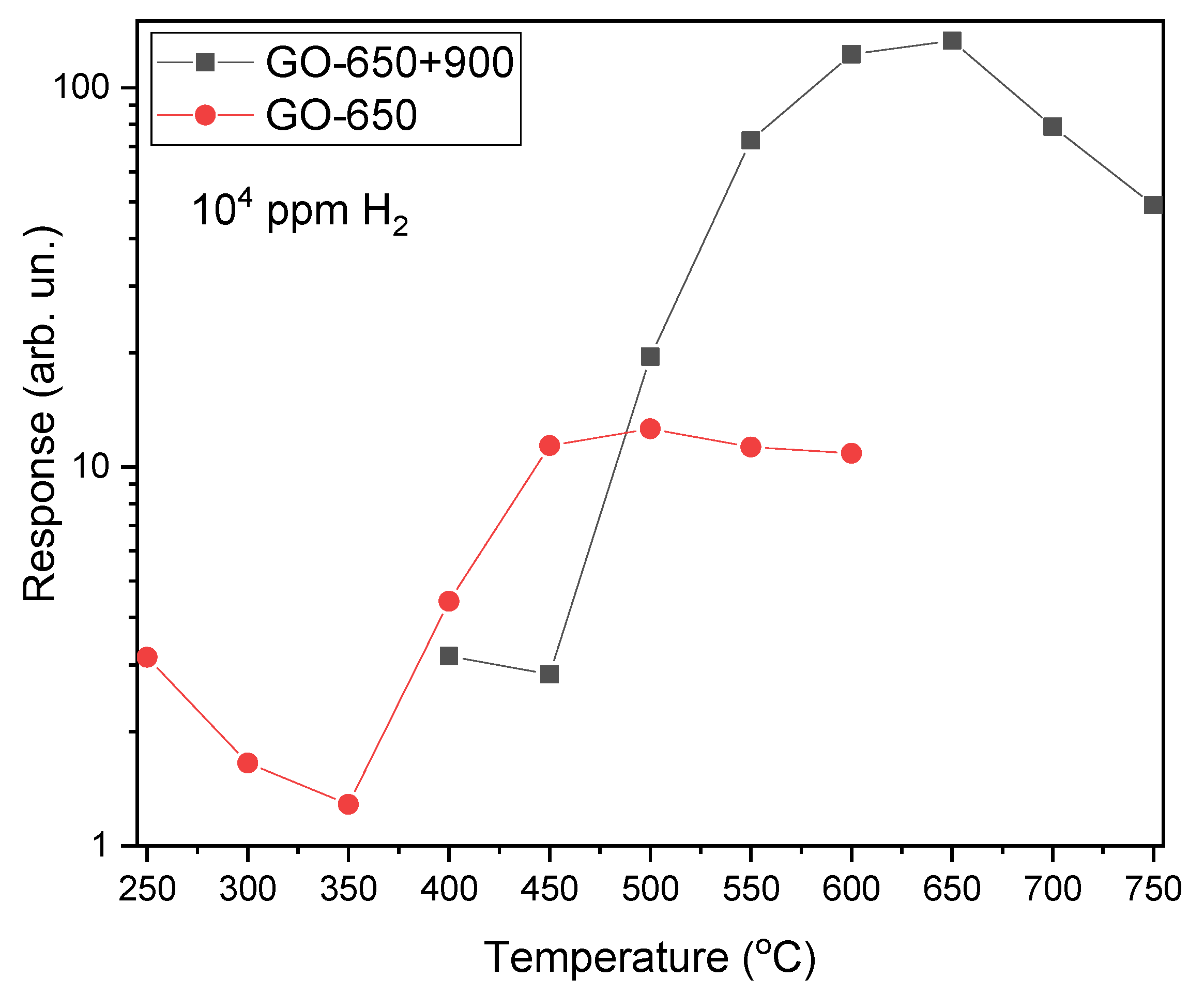
Figure 1 shows the dependence of responses to fixed H
2 concentrations on temperature for GO-650 and GO-650+900 thin films. Exposure to reducing gases H
2, CH
4, NH
3 and CO results in a reversible increase in current through the samples.
The following relationship was chosen as a reaction to reducing gases:
where
Ig is the current of a thin film in a gas mixture of pure dry air + reducing gas, and
Iair is the thin film current in pure dry air. Exposure to O
2, NO
2 leads to a reversible decrease in the current in the GO-650 and GO-650+900 samples. The following relationship was used to examine the response to these gases:
where
Iox is the current of a thin film in a gas mixture of pure dry air + oxidizing gas. The curves in
Figure 1 are characterized by the presence of maxima
SMAX at a certain temperature
TMAX. It is recommended to select
TMAX as the operating temperature.
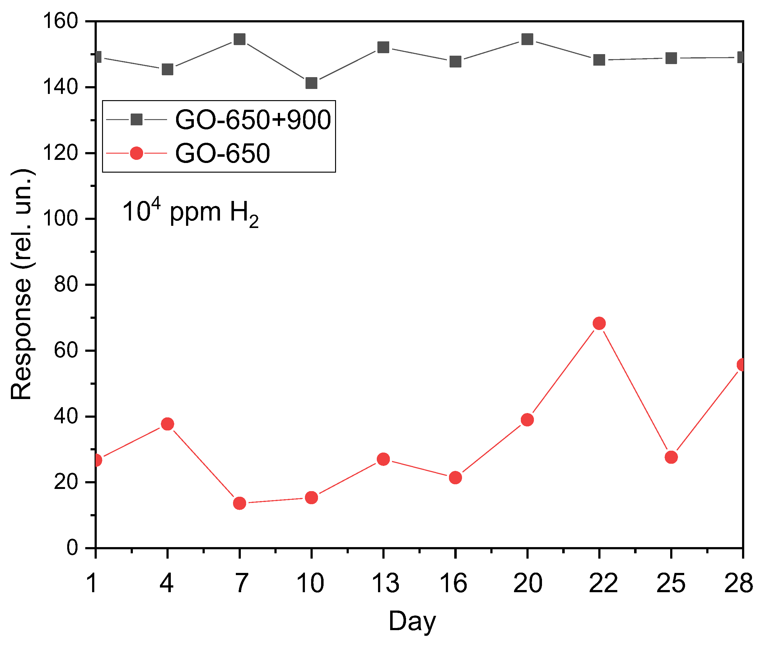
The response of GO-650 films when stored in a sealed bag after exposure to H
2 changes significantly. This results in a significant increase in response. Such a drift of gas-sensitive characteristics over time is typical for thin films of metal oxides and semiconductors. For sample GO-650+900, such a pattern is not observed, and the response deviates from the average value in small areas (
Figure 2).
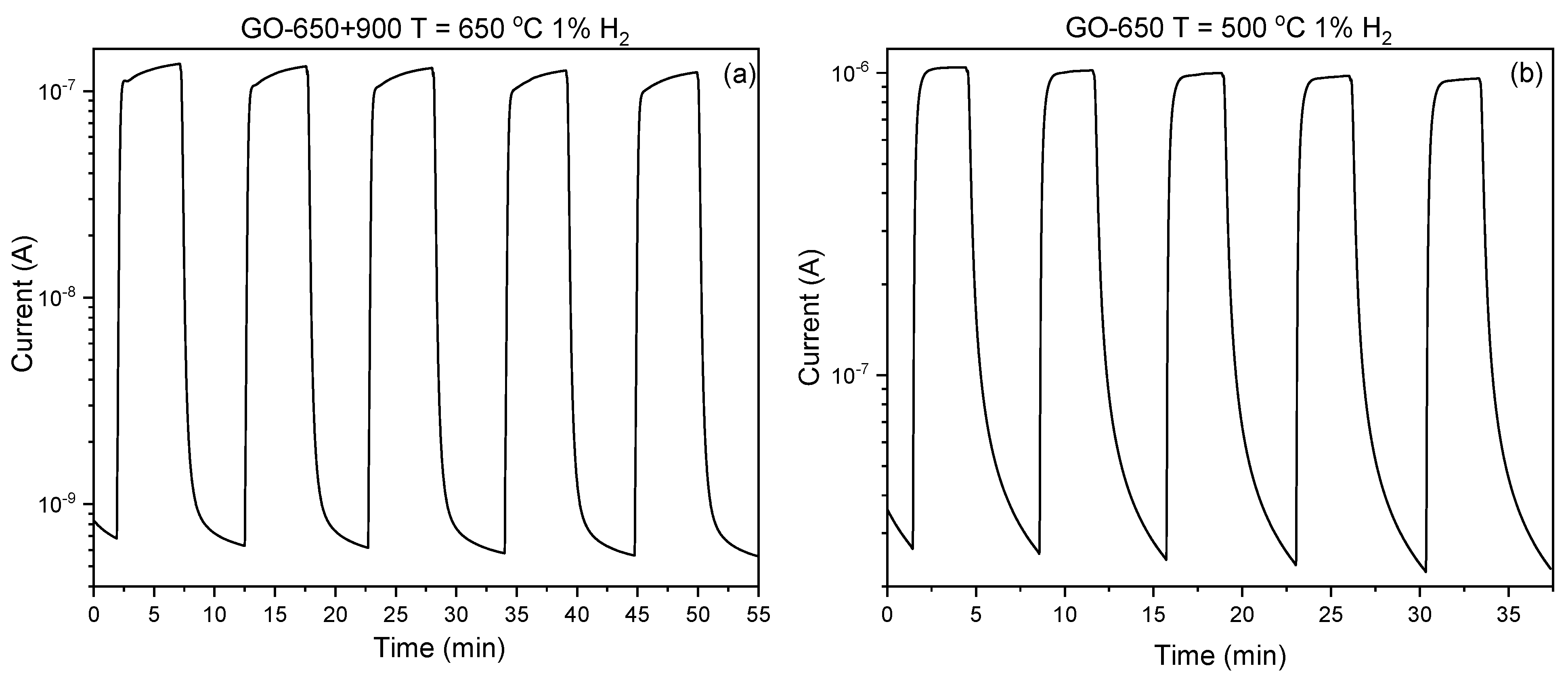
Despite the poor long-term stability of the GO-650 samples, all samples have good temporary stability over the course of a single experiment.
Figure 3 shows the time dependencies of the current under five-fold exposure to 1% of H
2.
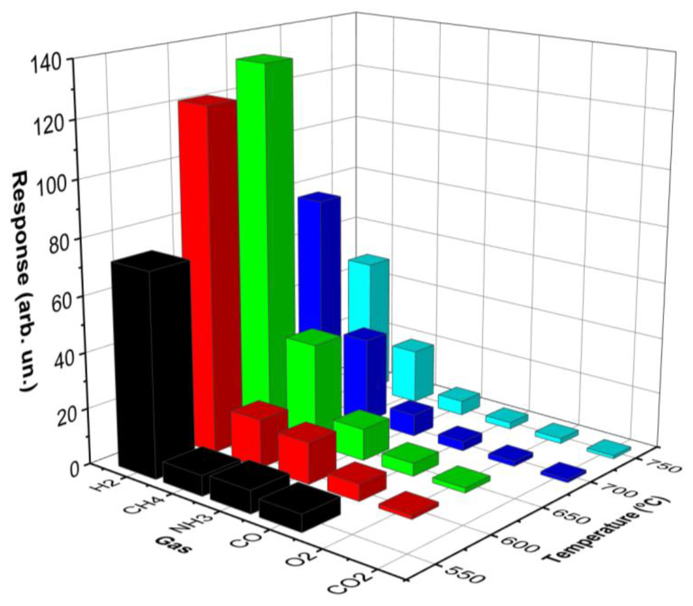
The selectivity of thin films was measured. The temperature dependencies of the response for various gases for GO-650+900 thin films are presented in
Figure 4.
The concentration of CH4, CO2 and O2 was 1 vol. %, the concentration of CO and NH3 was 0.2 vol. %. GO-650 thin films do not respond well to other gases. GO-650+900 samples have a high response to H2, NH3 and CH4.
The improvement in the gas-sensitive characteristics of GO-650+900 thin films is mainly due to annealing in an air atmosphere. As a result of annealing, the number of oxygen vacancies decreased, as evidenced by a decrease in the current density. The current density of the GO-650 samples is 0.10 A/cm2, and the current density of the GO-650+900 samples is 6.27 × 10⁻⁵ A/cm2. The current density was calculated at T = 500 °C. The stability of the GO-650+900 samples was also affected by the formation of interdigitated contacts.
4. Mechanism of Gas Sensitivity
In the air, oxygen is chemisorbed on the surface of gallium oxide, which captures electrons from the conduction band of gallium oxide, forming in the near-surface region of the semiconductor, a layer depleted of major charge carriers and electrons. Oxygen chemisorbed on the surface of β-Ga2O3 films is presented in molecular O2−, atomic O− and O2− forms. The atomic form of chemisorbed oxygen O− is the most reactive when interacting with molecules of reducing gases. In the temperature range of 200–650 °C, O− predominates on the surface of β-Ga2O3.
Chemisorption of oxygen can be described by using the following expression:
where O
−ch is a chemisorbed oxygen ion. Superstoichiometric gallium atoms Ga
3+ on the surface of β-Ga
2O
3 can act as adsorption centers for oxygen. In the region of selected operating temperatures, when reducing gases appear in the air, their molecules interact with previously chemisorbed O
−ch. These interactions on the surface of β-Ga
2O
3 can be described by the following reactions:
When the surface of a semiconductor is exposed to oxidizing gases NO
2 and NO, the following reactions may occur:
Reactions (7) occur without the participation of O−ch ions; NO2 and NO molecules are chemisorbed onto a free adsorption center and capture electrons from the conduction band of β-Ga2O3. An additional negative charge on the surface of β-Ga2O3 leads to a greater increase in eφs and, consequently, to a decrease in conductivity and charge carrier current in β-Ga2O3.
5. Conclusions
For the first time, the gas-sensitive properties of β-Ga2O3 structures obtained via RF magnetron sputtering with heating of the substrate and subsequent high-temperature annealing have been studied. Thin films of β-Ga2O3 without subsequent high-temperature annealing had a 3–4 times lower response to hydrogen and had a long drift of characteristics compared to the β-Ga2O3 samples with subsequent high-temperature annealing. As a result of high-temperature annealing and the formation of interdigitated contacts, GO-650+900 thin films became more stable, and the responses increased several times. As a result of annealing in air at T = 900 °C in samples followed by high-temperature annealing, the number of vacancies decreases, the current density decreases by four orders of magnitude, and stability increases.


 ,
, 


