Feature Paper Collection in Thin Films

A topical collection in Coatings (ISSN 2079-6412). This collection belongs to the section "Thin Films".

Viewed by 41938

Editors


E-Mail Website
Collection Editor
Institute of Nanotechnology, Karlsruhe Institute of Technology (KIT), Hermann-von-Helmholtz-Platz 1, Bldg. 717, 76344 Eggenstein-Leopoldshafen, Germany
Interests: Li-ion batteries; Li-S batteries; all-solid-state batteries; pseudocapacitors; thin films; materials science; mesoporous materials; self-assembled nanostructures; structure-property relationships
Special Issues, Collections and Topics in MDPI journals

E-Mail Website
Collection Editor
Institute of Nanotechnology, Karlsruhe Institute of Technology (KIT), Hermann-von-Helmholtz-Platz 1, Bldg. 640, 76344 Eggenstein-Leopoldshafen, Germany
Interests: high-entropy ceramics; printed electronics; batteries; electrochemistry; semiconductors; thin films; materials science; structure-property relationships

Topical Collection Information

Dear Colleagues,

Oxides and non-oxides in thin-film form are technologically important materials with a variety of applications in energy storage and conversion, sensing, electronics, mechanics, optics and biomedicine, resulting from unique combinations of properties. Inorganic, organic, and hybrid inorganic-organic materials can be produced with a range of structures, compositions, and thicknesses by physical and chemical deposition methods (e.g., atomic layer deposition, pulsed laser deposition, chemical vapor deposition, chemical solution deposition, etc.), with low-cost solution processing routes being usually more flexible in terms of chemistry. Apart from interfacial engineering and compositional design, nanoscale structuring at different length scales—through “top-down” and “bottom-up” approaches—has been shown to be effective in tailoring the properties of thin-film materials. However, the characterization becomes increasingly difficult with decreasing film thickness, and often the lack of structure-property relationship understanding is an impediment to applications. This “Feature Paper Collection” is dedicated to advanced thin film structures and devices, with special emphasis placed on their preparation, characterization, and application in the energy field.

Potential topics include (but are not limited to):

  • Novel oxide and non-oxide materials in thin-film form
  • Preparation by chemical and physical methods
  • Micro- and nanostructuring
  • Surface and interface engineering
  • Advanced characterization techniques
  • Structure–composition–property relationships
  • Application in electrochemical energy storage devices (e.g., as protective surface coating on anode/cathode materials for bulk-type batteries or as active component in thin-film batteries), catalysis, solar cells, sensors, data storage, etc.

Dr. Torsten Brezesinski
Dr. Ben Breitung
Collection Editors

Manuscript Submission Information

Manuscripts should be submitted online at www.mdpi.com by registering and logging in to this website. Once you are registered, click here to go to the submission form. Manuscripts can be submitted until the deadline. All submissions that pass pre-check are peer-reviewed. Accepted papers will be published continuously in the journal (as soon as accepted) and will be listed together on the collection website. Research articles, review articles as well as short communications are invited. For planned papers, a title and short abstract (about 100 words) can be sent to the Editorial Office for announcement on this website.

Submitted manuscripts should not have been published previously, nor be under consideration for publication elsewhere (except conference proceedings papers). All manuscripts are thoroughly refereed through a single-blind peer-review process. A guide for authors and other relevant information for submission of manuscripts is available on the Instructions for Authors page. Coatings is an international peer-reviewed open access monthly journal published by MDPI.

Please visit the Instructions for Authors page before submitting a manuscript. The Article Processing Charge (APC) for publication in this open access journal is 2600 CHF (Swiss Francs). Submitted papers should be well formatted and use good English. Authors may use MDPI's English editing service prior to publication or during author revisions.

Published Papers (17 papers)

2024

Jump to: 2023, 2022, 2021

9 pages, 3131 KiB  
Article
Improved-Performance Amorphous Ga2O3 Photodetectors Fabricated by Capacitive Coupled Plasma-Assistant Magnetron Sputtering
by Yiming Liu, Chong Peng, Chang Liu, Cong Yu, Jiarui Guo, Yiyang Chang and Yi Zhao
Coatings 2024, 14(9), 1204; https://doi.org/10.3390/coatings14091204 - 19 Sep 2024
Viewed by 674
Abstract
Ga2O3 has received increasing interest for its potential in various applications relating to solar-blind photodetectors. However, attaining a balanced performance with Ga2O3-based photodetectors presents a challenge due to the intrinsic conductive mechanism of Ga2O [...] Read more.
Ga2O3 has received increasing interest for its potential in various applications relating to solar-blind photodetectors. However, attaining a balanced performance with Ga2O3-based photodetectors presents a challenge due to the intrinsic conductive mechanism of Ga2O3 films. In this work, we fabricated amorphous Ga2O3 (a-Ga2O3) metal–semiconductor–metal photodetectors through capacitive coupled plasma assisted magnetron sputtering at room temperature. Substantial enhancement in the responsivity is attained by regulating the capacitance-coupled plasma power during the deposition of a-Ga2O3. The proposed plasma energy generated by capacitive coupled plasma (CCP) effectively improved the disorder of amorphous Ga2O3 films. The results of X-ray photoelectron spectroscopy (XPS) and current-voltage tests demonstrate that the additional plasma introduced during the sputtering effectively adjust the concentration of oxygen vacancy effectively, exhibiting a trade-off effect on the performance of a-Ga2O3 photodetectors. The best overall performance of a-Ga2O3 photodetectors exhibits a high responsivity of 30.59 A/W, a low dark current of 4.18 × 10⁻¹¹, and a decay time of 0.12 s. Our results demonstrate that the introduction of capacitive coupled plasma during deposition could be a potential approach for modifying the performance of photodetectors. Full article
Show Figures

Figure 1

2023

Jump to: 2024, 2022, 2021

13 pages, 2587 KiB  
Article
Coupled Modeling of Anisotropic Stress-Induced Diffusion and Trapping of Nitrogen in Austenitic Stainless Steel during Nitriding and Thermal Annealing
by Teresa Moskaliovienė, Paulius Andriūnas and Arvaidas Galdikas
Coatings 2023, 13(2), 415; https://doi.org/10.3390/coatings13020415 - 12 Feb 2023
Cited by 1 | Viewed by 1605
Abstract
In this paper, nitrogen diffusion is investigated in single-crystalline austenitic stainless steel during modified layer formation and thermal annealing. A generalized system of diffusion equations is derived within a thermodynamic framework from Fick’s laws, which describe nitrogen flux under multiple driving forces, including [...] Read more.
In this paper, nitrogen diffusion is investigated in single-crystalline austenitic stainless steel during modified layer formation and thermal annealing. A generalized system of diffusion equations is derived within a thermodynamic framework from Fick’s laws, which describe nitrogen flux under multiple driving forces, including a concentration gradient and the gradient of hydrostatic stress. Trapping and detrapping phenomena are considered within this model, and nitrogen flux is distinguished depending on whether nitrogen is in a lattice or a trapping site. Furthermore, the effects of anisotropic elasticity in single-crystal austenitic stainless steel on the stress field are investigated. The proposed model is used to simulate the nitrogen transportation process in single-crystalline AISI 316L during ion beam nitriding and after isothermal annealing at three different crystalline orientations. The results of our theoretical predictions are compared with experimental results taken from the literature. It is shown that during isothermal annealing, nitrogen diffusion becomes significantly slower than during nitriding. The diffusion coefficient during the annealing process, compared with the nitriding process, decreases by factors of 4.3, 3.3, and 2.5 for the orientations (001), (011), and (111), respectively. Full article
Show Figures

Figure 1

9 pages, 3824 KiB  
Communication
Reconstructed Cd(0001) Surface Induced by Adsorption of Triphenyl Bismuth
by Mengmeng Bai, Zuo Li, Mingxia Shi, Minlong Tao, Kai Sun, Xiaotian Yang, Yufeng Zhang and Junzhong Wang
Coatings 2023, 13(2), 394; https://doi.org/10.3390/coatings13020394 - 8 Feb 2023
Viewed by 1531
Abstract
Largish molecules on metal surfaces may act as not only the building blocks of 2D self-assemblies, but also as the template to reshape the metal surfaces. Here, we report the molecular adsorption-induced formation of the periodic nanostripe arrays of substrate atoms through long-range [...] Read more.
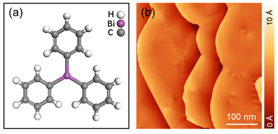
Largish molecules on metal surfaces may act as not only the building blocks of 2D self-assemblies, but also as the template to reshape the metal surfaces. Here, we report the molecular adsorption-induced formation of the periodic nanostripe arrays of substrate atoms through long-range mass transport. When adsorbed on the close-packed Cd(0001) surface, the triphenyl bismuth (TPB) molecules form a 2D self-assembly with 4 × √13 reconstruction. Simultaneously, periodic nanostripe arrays of Cd atoms appear on the substrate terraces. High-resolution scanning tunneling microscopy (STM) images indicate that the Cd nanostrips are built from the parallel segments of Cd atomic chains with 2 × 2 reconstruction. In the mixed phase, the Cd atomic chains exhibit only high-order commensuration when situated between two molecular domains. The massive structural rearrangement of the Cd(0001) surface can be attributed to a strong molecule–substrate interaction. Full article
Show Figures

Figure 1

13 pages, 6248 KiB  
Article
Study of Ion-Assisted E-Beam Evaporation Coating Process on Chirped Mirrors
by Yu-Long Chen and Pei-Jen Wang
Coatings 2023, 13(2), 356; https://doi.org/10.3390/coatings13020356 - 3 Feb 2023
Cited by 1 | Viewed by 2066
Abstract
A chirped mirror designed with 60 fs2 in group delay dispersion and reflectance large than 97.5% in the bandwidth between 700 and 900 nm by open-sourced thin film filter design software is presented. The chirped mirrors are then fabricated by an ion-assisted [...] Read more.
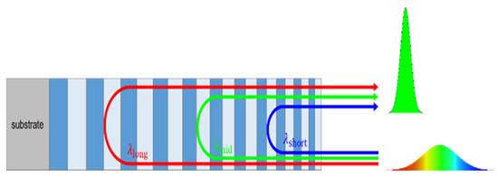
A chirped mirror designed with 60 fs2 in group delay dispersion and reflectance large than 97.5% in the bandwidth between 700 and 900 nm by open-sourced thin film filter design software is presented. The chirped mirrors are then fabricated by an ion-assisted deposition coater. First, the optical constants of the thin films deposited by specific process parameters are calibrated by trial runs with single-layer samples measured by variable-angle spectroscopic ellipsometer; then factors are entered to compensate for the settings on film thickness. Afterward, the spectral phase of the coated mirrors is measured by polarization gating frequency-resolved optical gating whereas the reflectance is measured by photo-spectrometer. In conclusion, the measured results indicate a reasonable match with the design goals to show the effectiveness of the proposed method. It is noted that ion-assisted electron gun evaporation coating systems are applicable to the mass production of chirped mirrors employed for ultrafast lasers. Full article
Show Figures

Figure 1

6 pages, 768 KiB  
Article
Characterisation of the Surface Free Energy of the Recycled Cellulose Layer that Comprises the Middle Component of Corrugated Paperboards
by János Keresztes and Levente Csóka
Coatings 2023, 13(2), 259; https://doi.org/10.3390/coatings13020259 - 22 Jan 2023
Cited by 2 | Viewed by 1470
Abstract
The objective of this study was to determine the polar and dispersive surface free-energy (SFE) components of the central layer of corrugated paperboards, which are made of recycled fibres. The polar and dispersive components of, and the total, SFE (also known as interfacial [...] Read more.
The objective of this study was to determine the polar and dispersive surface free-energy (SFE) components of the central layer of corrugated paperboards, which are made of recycled fibres. The polar and dispersive components of, and the total, SFE (also known as interfacial energy) were calculated from the contact angles of water and diiodomethane liquids on recycled cellulose sheets. The total SFE of the middle component layers of two different grammages which comprised recycled fibres ranged from 47.9 mN/m to 51.05 mN/m. The contribution of the polar component to the total surface free energy of the two types of sheets ranged from 8.6 mN/m to 12.6 mN/m. This polar contribution was significantly lower than that of water. The contact angle method proved to be a consistent way to estimate the surface properties of industrially made recycled paper products. Full article
Show Figures

Figure 1

9 pages, 2250 KiB  
Article
Dual-Type Flexible-Film Thermoelectric Generators Using All-Carbon Nanotube Films
by Ryota Konagaya and Masayuki Takashiri
Coatings 2023, 13(1), 209; https://doi.org/10.3390/coatings13010209 - 16 Jan 2023
Cited by 6 | Viewed by 2907
Abstract
The long-term stability of n-type single-walled carbon nanotubes (SWCNTs) in air makes all-carbon thermoelectric generators (TEGs) viable. To increase the performance of TEGs, we developed a dual-type flexible-film thermoelectric generator (DFTEG). The vacuum filtering was used to form p- and n-type SWCNT films [...] Read more.
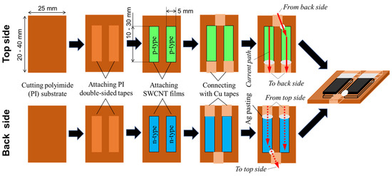
The long-term stability of n-type single-walled carbon nanotubes (SWCNTs) in air makes all-carbon thermoelectric generators (TEGs) viable. To increase the performance of TEGs, we developed a dual-type flexible-film thermoelectric generator (DFTEG). The vacuum filtering was used to form p- and n-type SWCNT films from ethanol-based dispersion and water-based solutions with cationic surfactant, respectively. DFTEGs were fabricated as follows: strip-shaped p- and n-type SWCNT films were attached on the top and back sides of a polyimide substrate, respectively, and were connected alternately in series by bending copper tapes on the edge of the polyimide substrate. The thermoelectric performance was measured after attaching the DFTEG outside a beaker full of water, where the water surface reached the center of the DFTEG. For a 10 mm long film and 15 p-n pairs, the DFTEG had an output voltage of 40 mV and a maximum power of 891 nW at a temperature difference of 25 K. The measured thermoelectric performance was significantly higher than that of the single-type TEG for almost the same SWCNT films. This result demonstrates that thermoelectric performance can be improved by using DFTEGs that are fabricated with optimum structural designs. Full article
Show Figures

Figure 1

21 pages, 12137 KiB  
Article
Impact of Microstructure of Nanoscale Magnetron Sputtered Ru/Al Multilayers on Thermally Induced Phase Formation
by Vincent Ott, Christian Schäfer, Sebastian Suarez, Karsten Woll, Frank Mücklich, Hans J. Seifert, Sven Ulrich, Christoph Pauly and Michael Stueber
Coatings 2023, 13(1), 149; https://doi.org/10.3390/coatings13010149 - 11 Jan 2023
Cited by 4 | Viewed by 1606
Abstract
In this study, we report on phase formation and microstructure evolution in multiscale magnetron sputtered Ru/Al multilayers upon thermal annealing in vacuum at slow heating rates of 10 K/min. By specifically adjusting the microstructure and design of the as-deposited multilayers, the formation of [...] Read more.
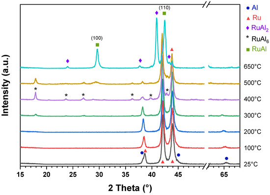
In this study, we report on phase formation and microstructure evolution in multiscale magnetron sputtered Ru/Al multilayers upon thermal annealing in vacuum at slow heating rates of 10 K/min. By specifically adjusting the microstructure and design of the as-deposited multilayers, the formation of certain desired phases can be tuned. We demonstrate that the synthesis of single phase RuAl thin films is possible in a very controlled manner in a solid state only via thermal activation without initiating the self-propagating exothermic reactions of Ru/Al multilayers. To investigate phase formation sequences and the resulting microstructures, Ru/Al multilayers were designed via magnetron sputtering with systematic variation of bilayer modulation periods and subsequent vacuum annealing. Thin films samples were characterized by in situ high-temperature XRD, TEM imaging and diffraction. It is shown that different phase sequences appear in strong correlation with the modulation length. Depending on the multilayer design, the phase formation toward single-phase RuAl thin films happens as either a multi-step or single-step event. In particular, below a critical threshold of the modulation period, the multi-step phase formation can be suppressed, and only the desired RuAl target phase is obtained with a pronounced growth in a preferred orientation. This finding may be versatile for the targeted synthesis of intermetallic phases, contributing to further understanding of phase formation in such nanoscale multilayer systems. Full article
Show Figures

Figure 1

2022

Jump to: 2024, 2023, 2021

13 pages, 2059 KiB  
Review
Metal-Doped TiO2 Thin Film as an Electron Transfer Layer for Perovskite Solar Cells: A Review
by Dewi Suriyani Che Halin, Ayu Wazira Azhari, Mohd Arif Anuar Mohd Salleh, Nur Izzati Muhammad Nadzri, Petrica Vizureanu, Mohd Mustafa Al Bakri Abdullah, Juyana A. Wahab and Andrei Victor Sandu
Coatings 2023, 13(1), 4; https://doi.org/10.3390/coatings13010004 - 20 Dec 2022
Cited by 10 | Viewed by 3626
Abstract
The electron transfer layer (ETL) plays a vital role in achieving high-performance perovskite solar cells (PSCs). Titanium dioxide (TiO2) is primarily utilised as the ETL since it is low-cost, chemically stable, and has the simplest thin-film preparation methods. However, TiO2 [...] Read more.
The electron transfer layer (ETL) plays a vital role in achieving high-performance perovskite solar cells (PSCs). Titanium dioxide (TiO2) is primarily utilised as the ETL since it is low-cost, chemically stable, and has the simplest thin-film preparation methods. However, TiO2 is not an ideal ETL because it leads to low conductivity, conduction band mismatch, and unfavourable electron mobility. In addition, the exposure of TiO2 to ultraviolet light induces the formation of oxygen vacancies at the surface. To overcome these issues, doping TiO2 with various metal ions is favourable to improve the surface structure properties and electronic properties. This review focuses on the bulk modification of TiO2 via doping with various metal ions concentrations to improve electrical and optical properties, charge carrier density, and interfacial electron–hole recombination, thus contributing to enhancing the power conversion efficiency (PCE) of the PSCs. Full article
Show Figures

Figure 1

14 pages, 4015 KiB  
Article
Chemical Stability of Sputter Deposited Silver Thin Films
by Diederik Depla
Coatings 2022, 12(12), 1915; https://doi.org/10.3390/coatings12121915 - 7 Dec 2022
Cited by 5 | Viewed by 2979
Abstract
Silver films with a thickness below 50 nanometer were deposited on glass using DC magnetron sputtering. The chemical stability of the films was investigated by exposure of the film to a droplet of a HCl solution in a humid atmosphere. The affected area [...] Read more.
Silver films with a thickness below 50 nanometer were deposited on glass using DC magnetron sputtering. The chemical stability of the films was investigated by exposure of the film to a droplet of a HCl solution in a humid atmosphere. The affected area was monitored with a digital microscope. The affected area increases approximately linearly with time which points to a diffusive mechanism. The slope of the area versus time plot, or the diffusivity, was measured as a function of the acid concentration, the presence of an aluminum seed layer, and film thickness. The diffusivity scales linearly with the acid concentration. It is shown that the diffusivity for Al-seeded Ag films is much lower. The behavior as function of the film thickness is more complex as it shows a maximum. Full article
Show Figures

Figure 1

12 pages, 1689 KiB  
Article
Colloidal Aqueous Dispersions of Methyl (meth)Acrylate-Grafted Polyvinyl Alcohol Designed for Thin Film Applications
by Silvia Bozhilova, Katerina Lazarova, Sijka Ivanova, Daniela Karashanova, Tsvetanka Babeva and Darinka Christova
Coatings 2022, 12(12), 1882; https://doi.org/10.3390/coatings12121882 - 3 Dec 2022
Cited by 2 | Viewed by 1985
Abstract
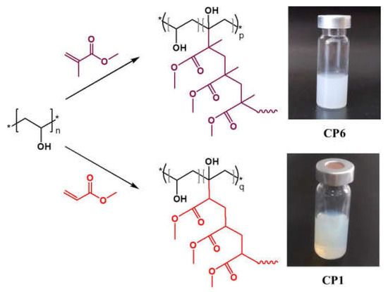
In this paper, the aqueous copolymer dispersions of methyl (meth)acrylate-grafted poly(vinyl alcohol) are in situ synthesized and studied as a promising platform for the deposition of thin films with advanced applications. A series of dispersions of the varied copolymer structure and composition are [...] Read more.
In this paper, the aqueous copolymer dispersions of methyl (meth)acrylate-grafted poly(vinyl alcohol) are in situ synthesized and studied as a promising platform for the deposition of thin films with advanced applications. A series of dispersions of the varied copolymer structure and composition are obtained at mild reaction conditions by carrying out a redox polymerization at a different monomer-to-PVA ratio and initiator concentration. The obtained colloidal particles are characterized by Fourier transformed infrared spectroscopy, nuclear magnetic resonance, dynamic light scattering, and transmission electron microscopy. The copolymer dispersions are further used for deposition of thin films on silicon substrates. The films are characterized optically through reflectance measurements and non-linear curve fitting. Their suitability for the optical sensing of acetone vapors is confirmed by reflectance measurements before and during their exposure to analyte vapors. The cross sensitivity, sensing repeatability, and recovery of the sensitive films are discussed. Full article
Show Figures

Figure 1

21 pages, 16125 KiB  
Article
Influence of Fluorine and Nitrogen Co-Doping on the Structural and Morphological Properties of Sol-Gel ZnO Films
by Tatyana Ivanova, Antoaneta Harizanova, Tatyana Koutzarova, Benedicte Vertruyen and Raphael Closset
Coatings 2022, 12(12), 1874; https://doi.org/10.3390/coatings12121874 - 2 Dec 2022
Cited by 1 | Viewed by 1733
Abstract
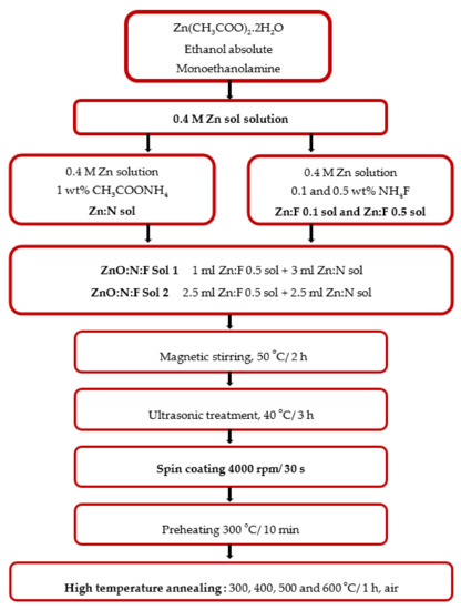
The structural, vibrational, optical and morphological properties of ZnO:N:F films, obtained by the sol-gel method, were investigated. The effect of single (fluorine, nitrogen) and F, N co-doping and thermal treatments (300–600 °C) on the properties of ZnO films was analyzed. X-ray Diffraction (XRD) [...] Read more.
The structural, vibrational, optical and morphological properties of ZnO:N:F films, obtained by the sol-gel method, were investigated. The effect of single (fluorine, nitrogen) and F, N co-doping and thermal treatments (300–600 °C) on the properties of ZnO films was analyzed. X-ray Diffraction (XRD) revealed that ZnO:N:F films crystallized in a polycrystalline wurtzite structure. F and N incorporation changed lattice parameters, crystallite sizes, texture coefficients (TC) and residual stress. TC (002) of ZnO:N:F films increased with annealing, reaching 1.94 at 600 °C lower than the TC (002) of ZnO and ZnO:N films. The shifting of the characteristic absorption bands and/or the appearance of new IR lines were detected for ZnO:N:F samples. The highest transmittance (90.98%) in the visible spectral region was found for ZnO:F films. ZnO:N:F films possessed optical transparency up to 88.18% and their transmittance decreased at the higher annealings. The optical band gap (Eg) values of ZnO:N:F films were changed with fluorine and nitrogen concentrations. The formation of the wrinkle-like structures on the surface of ZnO and ZnO:N films was depicted in Field Emission Scanning Electron Microscopy (FESEM) images. The F, N dual doping modified ZnO morphology and suppressed wrinkle formation. Full article
Show Figures

Figure 1

14 pages, 4407 KiB  
Article
Synthesis of High Quality Transparent Nanocrystalline Diamond Films on Glass Substrates Using a Distributed Antenna Array Microwave System
by Chaimaa Mahi, Ovidiu Brinza, Riadh Issaoui, Jocelyn Achard and Fabien Bénédic
Coatings 2022, 12(10), 1375; https://doi.org/10.3390/coatings12101375 - 20 Sep 2022
Cited by 5 | Viewed by 2249
Abstract
Diamond is a material of choice for the fabrication of optical windows and for protective and anti-reflecting coatings for optical materials. For these kinds of applications, the diamond coating must have a high purity and a low surface roughness to guarantee a high [...] Read more.
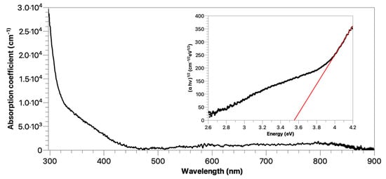
Diamond is a material of choice for the fabrication of optical windows and for protective and anti-reflecting coatings for optical materials. For these kinds of applications, the diamond coating must have a high purity and a low surface roughness to guarantee a high transparency. It should also be synthesized at low surface temperature to allow the deposition on low melting-point substrates such as glasses. In this work, the ability of a Distributed Antenna Array (DAA) microwave system operating at low temperature and low pressure in H2/CH4/CO2 gas mixture to synthesize nanocrystalline diamond (NCD) films on borosilicate and soda-lime glass substrates is investigated aiming at optical applications. The influence of the substrate temperature and deposition time on the film microstructure and optical properties is examined. The best film properties are obtained for a substrate temperature below 300 °C. In these conditions, the growth rate is around 50 nm·h−1 and the films are homogeneous and formed of spherical aggregates composed of nanocrystalline diamond grains of 12 nm in size. The resulting surface roughness is then very low, typically below 10 nm, and the diamond fraction is higher than 80%. This leads to a high transmittance of the NCD/glass systems, above 75%, and to a low absorption coefficient of the NCD film below 103 cm−1 in the visible range. The resulting optical band gap is estimated at 3.55 eV. The wettability of the surface evolves from a hydrophilic regime on the bare glass substrates to a more hydrophobic regime after NCD deposition, as assessed by the increase of the measured contact angle from less than 55° to 76° after the deposition of 100 nm thick NCD film. This study emphasizes that such transparent diamond films deposited at low surface temperature on glass substrate using the DAA microwave technology can find applications for optical devices. Full article
Show Figures

Graphical abstract

9 pages, 4329 KiB  
Article
Study on Deuterium Permeation Behavior of Palladium Films Prepared by Magnetron Sputtering Method
by Zhihao Hong, Long Wang, Yongjin Feng, Baoping Gong, Jijun Yang and Xiaoyu Wang
Coatings 2022, 12(7), 978; https://doi.org/10.3390/coatings12070978 - 10 Jul 2022
Cited by 1 | Viewed by 1638
Abstract
Pre-depositing a Pd film is crucial for accurately acquiring the hydrogen permeability of metal materials, as it permits the production of ultra-pure hydrogen. However, the microstructure of Pd film and its effect on the hydrogen isotope permeation behavior of substrate materials have been [...] Read more.
Pre-depositing a Pd film is crucial for accurately acquiring the hydrogen permeability of metal materials, as it permits the production of ultra-pure hydrogen. However, the microstructure of Pd film and its effect on the hydrogen isotope permeation behavior of substrate materials have been neglected. In this study, Pd films were deposited on China Low-activation Ferritic (CLF−1) steel by magnetron sputtering. The effect of sputtering pressure on the microstructure and deuterium permeation behavior of Pd films at temperatures of 550−650 °C is presented. SEM results demonstrated that the films had a columnar crystal structure with a thickness of 0.6 ± 0.2 μm. The gas-driven permeation results revealed that the deuterium ion current intensity of the coated CLF−1 sample was at least three times lower than that of uncoated CLF−1 steel, which was influenced by the combined effect of oxygen and surface cracks. Oxygen could not be excluded from the films at a sputtering pressure of 10−3 Pa order of magnitude. It was also found that the films cracked during deuterium permeation experiments, which affected the deuterium permeation behavior. Films with large surface coverage and small grain sizes exhibited better cracking resistance. Our study provides promising insights into the hydrogen permeability of Pd films. Full article
Show Figures

Figure 1

11 pages, 2785 KiB  
Article
Diffusion Barrier Characteristics of WSiN Films
by Yung-I Chen, Kuo-Hong Yeh, Tzu-Yu Ou and Li-Chun Chang
Coatings 2022, 12(6), 811; https://doi.org/10.3390/coatings12060811 - 10 Jun 2022
Cited by 3 | Viewed by 2547
Abstract
WSiN films were produced through hybrid pulse direct current/radio frequency magnetron co-sputtering and evaluated as diffusion barriers for Cu metallization. The Cu/WSiN/Si assemblies were annealed for 1 h in a vacuum at 500–900 °C. The structural stability and diffusion barrier performance of the [...] Read more.
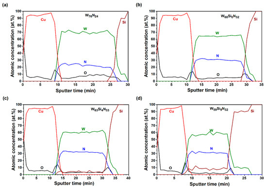
WSiN films were produced through hybrid pulse direct current/radio frequency magnetron co-sputtering and evaluated as diffusion barriers for Cu metallization. The Cu/WSiN/Si assemblies were annealed for 1 h in a vacuum at 500–900 °C. The structural stability and diffusion barrier performance of the WSiN films were explored through X-ray diffraction, Auger electron spectroscopy, and sheet resistance measurement. The results indicated that the Si content of WSiN films increased from 0 to 9 at.% as the power applied to the Si target was increased from 0 to 150 W. The as-deposited W76N24, W68Si0N32, and W63Si4N33 films formed a face-centered cubic W2N phase, whereas the as-deposited W59Si9N32 film was near-amorphous. The lattice constants of crystalline WSiN films decreased after annealing. The sheet resistance of crystalline WSiN films exhibited a sharp increase as they were annealed at 800 °C, accompanied by the formation of a Cu3Si compound. The failure of the near-amorphous W59Si9N32 barrier against Cu diffusion was observed when annealed at 900 °C. Full article
Show Figures

Figure 1

24 pages, 6768 KiB  
Article
Preparation of Very Thin Zinc Oxide Films by Liquid Deposition Process: Review of Key Processing Parameters
by Mouna Khiari, Mickaël Gilliot, Michaël Lejeune, Florica Lazar and Aomar Hadjadj
Coatings 2022, 12(1), 65; https://doi.org/10.3390/coatings12010065 - 6 Jan 2022
Cited by 8 | Viewed by 4096
Abstract
We used sol-gel and spin-coating in the original configuration of a liquid deposition process to synthesize particularly thin ZnO films (<100 nm) with nano-granular morphology, high grain orientation and variable optical properties. The concentration of the zinc salt, the concentration of the chelating [...] Read more.
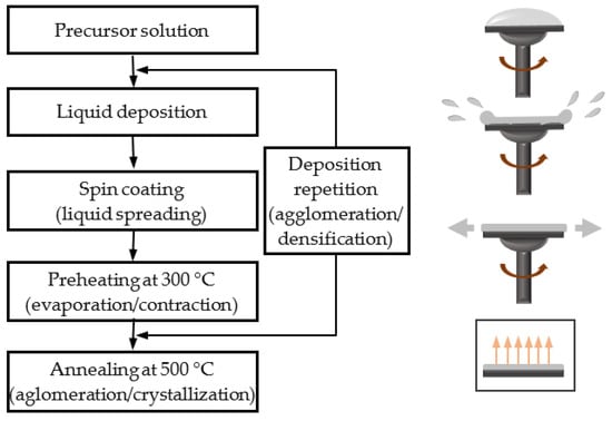
We used sol-gel and spin-coating in the original configuration of a liquid deposition process to synthesize particularly thin ZnO films (<100 nm) with nano-granular morphology, high grain orientation and variable optical properties. The concentration of the zinc salt, the concentration of the chelating agent, the nature of the solvent and the substrate material have been identified as key parameters that determine the microstructure of the deposited layer and thus its final properties. The thorough and practical examination of the effects of the synthesis parameters evidenced a three-step growth mechanism for these ZnO thin films: (i) a reaction of precursors, (ii) a formation of nuclei, and (iii) a coalescence of nanoparticles under thermal annealing. The growth of these very thin films is thus conditioned by the interaction between the liquid phase and the substrate especially during the initial steps of the spin coating process. Such thin ZnO films with such nano-granular morphology may be of great interest in various applications, especially those requiring a large active surface area. Full article
Show Figures

Figure 1

2021

Jump to: 2024, 2023, 2022

9 pages, 18837 KiB  
Article
Tuning the Electrical Properties of NiO Thin Films by Stoichiometry and Microstructure
by Yu-He Liu, Xiao-Yan Liu, Hui Sun, Bo Dai, Peng Zhang and Yong Wang
Coatings 2021, 11(6), 697; https://doi.org/10.3390/coatings11060697 - 10 Jun 2021
Cited by 2 | Viewed by 3326
Abstract
Here, the electrical properties of NiO thin films grown on glass and Al2O3 (0001) substrates have been investigated. It was found that the resistivity of NiO thin films strongly depends on oxygen stoichiometry. Nearly perfect stoichiometry yields extremely high resistivity. [...] Read more.
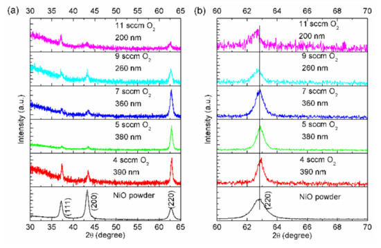
Here, the electrical properties of NiO thin films grown on glass and Al2O3 (0001) substrates have been investigated. It was found that the resistivity of NiO thin films strongly depends on oxygen stoichiometry. Nearly perfect stoichiometry yields extremely high resistivity. In contrast, off-stoichiometric thin films possess much lower resistivity, especially for oxygen-rich composition. A side-by-side comparison of energy loss near the edge structure spectra of Ni L3 edges between our NiO thin films and other theoretical spectra rules out the existence of Ni3+ in NiO thin films, which contradicts the traditional hypothesis. In addition, epitaxial NiO thin films grown on Al2O3 (0001) single crystal substrates exhibit much higher resistivity than those on glass substrates, even if they are deposited simultaneously. This feature indicates the microstructure dependence of electrical properties. Full article
Show Figures

Figure 1

18 pages, 24654 KiB  
Article
Influence of the Physical Properties on the Antibacterial and Photocatalytic Behavior of Ag-Doped Indium Sulfide Film Deposited by Spray Pyrolysis
by Belgacem Tiss, Youssef Moualhi, Noureddine Bouguila, Mabrouk Kraini, Sahbi Alaya, Catalin Croitoru, Ioana Ghiuta, Daniel Cristea, Delia Patroi, Cacilda Moura and Luís Cunha
Coatings 2021, 11(4), 370; https://doi.org/10.3390/coatings11040370 - 24 Mar 2021
Cited by 9 | Viewed by 3379
Abstract
Spray pyrolysis was used to deposit indium sulfide (In2S3) films, with or without silver doping. The films are polycrystalline, and the inclusion of Ag in the In2S3 structure leads to the formation of a solid solution, [...] Read more.
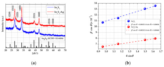
Spray pyrolysis was used to deposit indium sulfide (In2S3) films, with or without silver doping. The films are polycrystalline, and the inclusion of Ag in the In2S3 structure leads to the formation of a solid solution, with the crystallite size of the order of tens of nanometers. In2S3 films exhibit a semiconductive behavior, and the incorporation of Ag leads to an increase of the charge carrier concentration, enhancing the electrical conductivity of the films. The small polaron hopping mechanism, deduced by the fittings according to the double Jonscher variation, explains the evolution of the direct current (dc) conductivity at high temperature of the Ag-doped indium sulfide. From impedance spectroscopy, it was found that the doped film presents dielectric relaxation, and Nyquist diagrams indicate the importance of the grain and the grain boundaries’ contributions to the transport phenomena. The physical characteristics of the films have an influence on the photocatalytic performance, achieving photodegradation efficiency above 80% (85.5% in the case of Ag doping), and on the antibacterial activity. The obtained results indicate that indium sulfide films are good candidates for environmental and biological applications, confirming a multifunctional nature. Full article
Show Figures

Figure 1

Back to TopTop