1. Introduction
The Wireless Power Transfer (WPT) system as a novel technology can realize power wireless transmission from power supply to electrical equipment with the aid of magnetic coupling. With its rapid development, more and more applications have appeared in electrical vehicles, biomedical implants and cell phone areas [
1,
2,
3,
4,
5,
6].
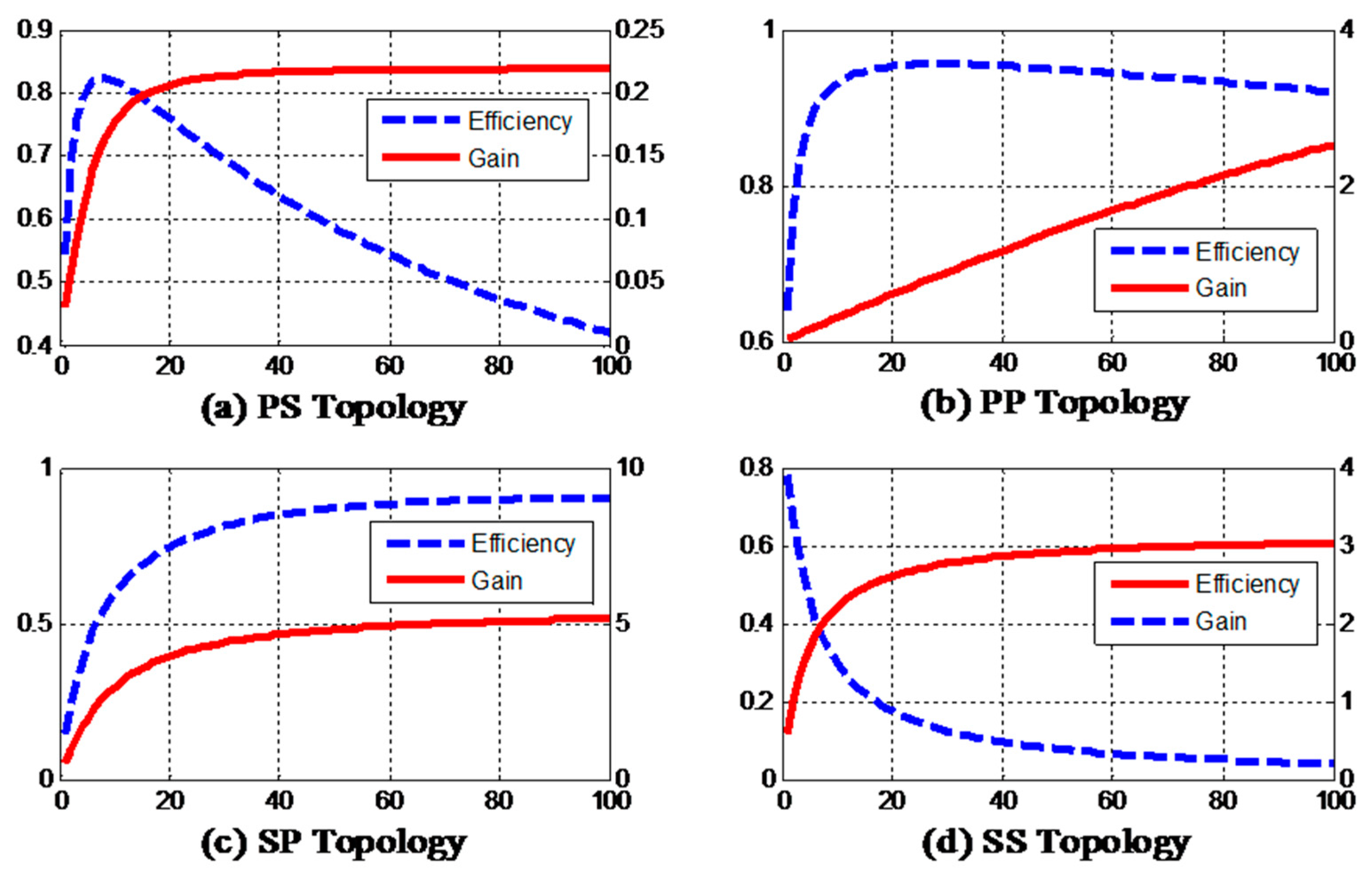
More and more applications in WPT technology require low DC voltage input and high voltage output. These applications include the Photovoltaic (PV) system, battery power supply system and Universal Serial Bus (USB) powered devices. However, it is not easy for the WPT system to obtain high voltage gain according to the following reasons—first, due to the WPT system being a weakly coupling system with very low coupling coefficient k (normally below 0.2) [
7,
8] and the coupling coefficient of transformer can almost reach 1. The second reason is the inherent characteristic of the resonant network. There are four fundamental resonant topologies SS, SP, PS, and PP (S and P denotes series and parallel topology, respectively). Series resonant network exhibits voltage source characteristics that cannot obtain a high voltage gain. The parallel resonant network exhibits current source characteristics that obtain high voltage gain on the light load condition. However, for heavy load conditions, it still cannot obtain high voltage gain. Furthermore, its reflecting impedance will bring relatively large frequency drift, which may cause a large reduction in output power [
9,
10]. For the same reason, composite resonant networks such as Inductor Capacitor Inductor (LCL), Inductor Capacitor Capacitor (LCC), and Capacitor Inductor Capacitor (CLC), which are combinations of the series and resonant topology, cannot reach high voltage gain. Reference [
11] analyzes wireless charging circuit characteristics under hybrid compensation topology. The analysis results show that the output voltage gain is below three in hybrid compensation topology.
To achieve high output voltage gain, the classical method is implemented by placing an additional Boost converter at the primary or secondary side. However, the added Boost converter will increase the volume and weight of the whole system [
12,
13], and make the system complicated to control. There are few papers related with voltage gain improvement. Aiming at voltage gain optimization and control, Reference [
14] proposes a uniform voltage gain control method. This method is implemented by control system operating frequency. However, the method only aims at improving the robustness against misalignment. Reference [
15] proposes a detached magnetic core to improve the voltage gain method. The obtained voltage gain is 0.83. Reference [
16] proposes an S/SP topology converter to obtain constant voltage gain. However, the voltage gain cannot be adjusted and will be very sensitive to frequency drift on the high gain condition.
In order to obtain a high and controllable output voltage gain WPT system, this paper proposes a novel current-fed push–pull converter at the primary side. A pair of Insulated Gate Bipolar Transistor (IGBT) switches, which act as a directional switch, is added in front of the resonant network to isolate the inverter and resonant network. An energy storage and injection switching mode is proposed to control the energy flowing into the resonant network. A switching duty cycle regulation method is also proposed to reach high voltage gain.
2. High Output Gain Push–Pull Circuit
The proposed high output gain push–pull circuit is shown in
Figure 1. Compared with traditional push–pull circuits, the proposed circuit adds two additional switches
S3 and
S4 to form a bi-directional switch. At the primary side, a DC power supply is a series with an inductor to form a quasi-current source. A push–pull transformer including
L1 and
L2 is utilized to divide the DC current in half, so that the current flowing into the resonant tank is approximately a square waveform with half the magnitude of the input DC current. The primary side uses two main switches (
S1 and
S2) with a common ground and two auxiliary switches (
S3 and
S4) in series with a parallel-tuned resonant tank, which consists of a resonant capacitor
CP, a resonant inductor
LP and equivalent series resistance
RP. The secondary side comprises a parallel resonant tank, which consists of a resonant inductor
LS, equivalent series resistance
RS, and a resonant capacitor
CS. With the rectifier bridge (
D1–
D4) and Inductor Capacitor (LC) filter network, AC energy is transformed to DC output to the load
R.
Aiming at voltage gain promotion, this paper proposes a resonant energy promotion method at the primary side. An energy storage mode is realized by shorting the DC inductor and phase-shifting transformer. An energy injection mode is realized by combining the storage energy and DC input energy together and outputting to the resonant tank. The switching between the energy storage and injection mode is implemented by auxiliary switch pair S3 and S4.
Figure 2 shows fundamental operation principles of the proposed method. The pulses and current waveforms of the proposed circuit switches are shown.
VGE1 to
VGE4 denotes the driving signals of switches
S1 to
S4, respectively. The current waveform of
iL2 is similar to the current waveform of
iL1, except for half-cycle delay. The function of anti-series switches (
S3 and
S4) is to control the connection between resonant tank and push–pull circuit. During one full switching cycle, the circuit operation can be divided into the following four modes and can be shown in
Figure 3.
Mode I:
t0–
t1: In this mode, switches
S2 and
S4 are turned on; switches
S1 and
S3 are turned off. The operation of this mode is shown in
Figure 3a. The energy stored in
L1 is transfer into the resonant circuit by switch
S4 and the reverse diode of
S3; switch
S2 is remaining conduction, so that the current flowing
L2 is rising slowly and
L2 is still working in the state of storage.
Mode II:
t1–
t2: In this mode, switches
S1 and
S2 are turned on and switches
S3 and
S4 are turned off. The operation of this mode is shown in
Figure 3b. Switches
S3 and
S4 are turned off and the resonant circuit enters the state of free energy oscillation between
LP and
CP. Switches
S1 and
S2 are turned on and
L1 and
L2 are both working in the state of storage.
Mode III:
t2–
t3: In this mode, switches
S1 and
S3 are turned on; switches
S2 and
S4 are turned off. The operation of this mode is shown in
Figure 3c. The energy stored in
L2 is transferred into the resonant circuit by switch
S3 and the reverse diode of
S4 and the current flowing through
L2 is decreasing; switch
S1 is remaining conduction, so that the current flowing
L1 is rising slowly and
L1 is still working in the state of storage.
Mode IV:
t3–
t4: This mode is similarly with Mode II, switches
S1 and
S2 are turned on and switches
S3 and
S4 are turned off. The operation of this mode is shown in
Figure 3d. Switches
S3 and
S4 are turned off and the resonant circuit enters the state of free energy oscillation between
LP and
CP. Switches
S1 and
S2 are turned on and
L1 and
L2 are both working in the state of storage.
3. Voltage Gain Analysis
Assuming that the resonant cycle of the circuit is T, and the switching duty cycle of S1 and S2 is D; correspondingly, the duty cycle of S3 and S4 is (1 − D). According to the volt–second balance of inductors L1 and L2, the average voltage across L1 and L2 is equal to zero during one switching cycle period. During the steady state, the current flows through L1 and L2 is equal so that the energy stored in inductors L1 and L2 is equal as well. Next, the paper will calculate the output gain based on the fact that the energy stored and released in inductor L1 is equal during one switching cycle.
In the steady state, the supply current is
Id, and the current flowing through
L1 or
L2 is
Id/2. Assuming the resonant network terminal voltage is
UAB, thus the volt-second balance equation can be obtained as
Note that duty cycle of switches
S1 and
S2 is no less than 0.5. It is because when the duty cycle is less than 0.5, switches
S1 and
S2 will enter the state of turning off at the same time; correspondingly, switches
S3 and
S4 will enter the state of turning on. It will result that the current of
L1 and
L2 drops sharply to zero and the current will become discontinuities. On the assumption, system equivalent circuit can be shown as
Figure 4.
At the secondary side, according to the energy balance equation, the equivalent resistance
Req of DC part including rectifier, filter and load at the secondary side is
The reflection impendence from the secondary to primary side can be expressed by
where
ZS = (
jωLS +
RS) +
Req/(
jωCSReq + 1) is the input impendence of secondary resonant network. Its resonant angular frequency is
ω = 2π
f.
The input impendence of the push–pull network can be expressed as
The resonant current of the primary side
IP can be expressed as
It is well known that the inductive voltage source of secondary side can be expressed as
On the resonant condition
ω2LSCS = 1, the output voltage
VO the load can be obtained as
Therefore, the voltage gain of the proposed circuit can be expressed as Equation (9)
Equation (9) shows that the output voltage can be controlled by duty cycle D, coupling coefficient k, switching frequency f and the equivalent resistance Req. However, frequency f and the load R usually are constant in the proposed circuit, thus the output voltage can be regulated by the duty cycle D of the push–pull switches S1 and S2.
Compared with traditional full-bridge circuit, its equivalent AC input
UAB can be calculated by
In addition, the voltage gain of the full-bridge converter will be
As can be seen from Equations (9) and (11), we can draw a conclusion that the voltage gain of proposed topology can be at least two times than traditional full-bridge topology.
Compared with a traditional push–pull circuit, its equivalent AC input
UAB can be calculated by
Furthermore, the voltage gain of the full-bridge converter will be
As can be seen from Equations (9) and (13), we can draw a conclusion that the voltage gain of proposed topology can achieve times the traditional push–pull topology.
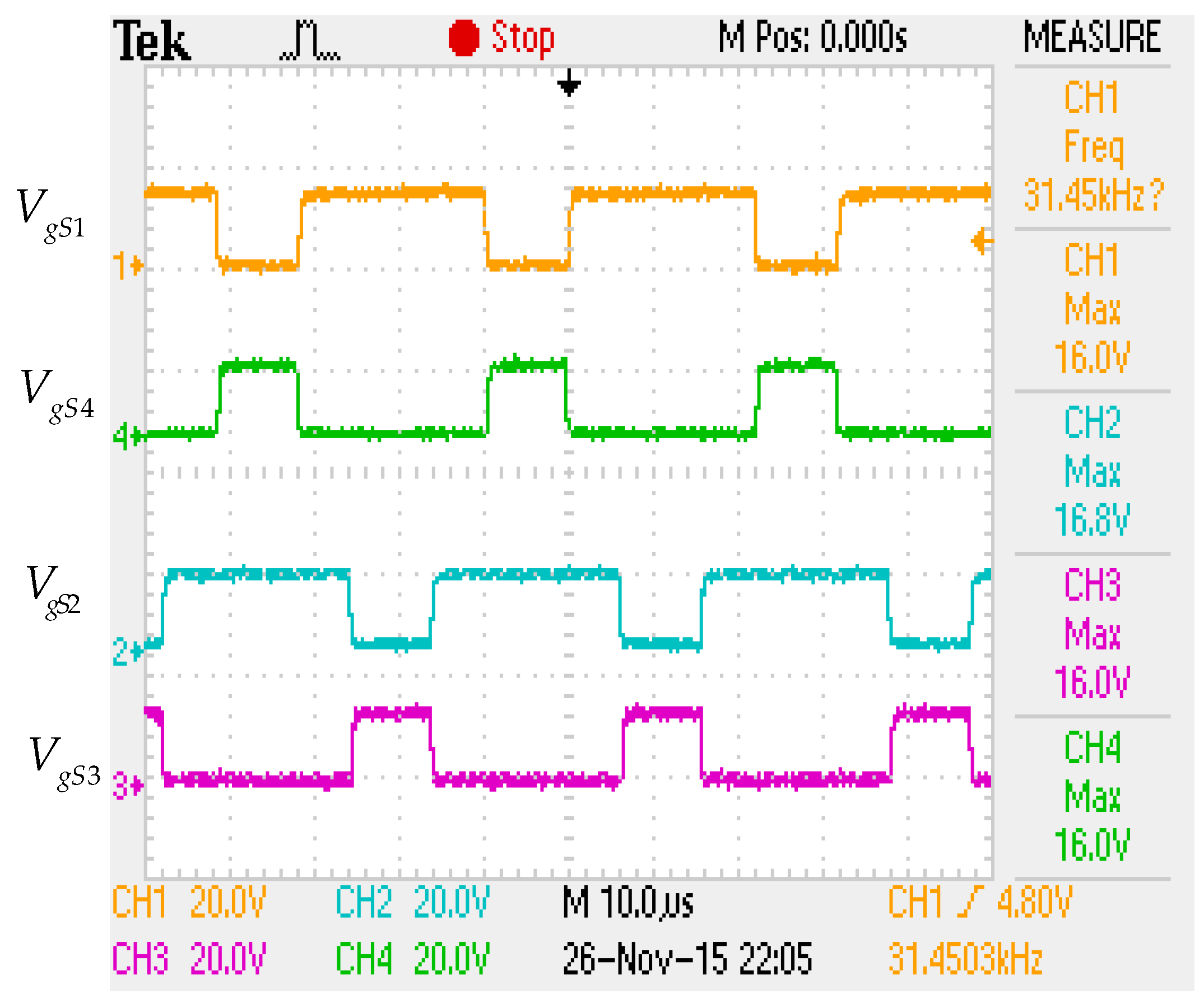
5. Experimental Verification
For the sake of verifying the performance of the proposed topology, a prototype system is built up. The system has been constructed according to the parameters provided in
Table 1 and the device photo is shown in
Figure 8.
Figure 9 shows the waveforms of the push–pull switches gate-driving signals and anti-series switching gate-driving signals. The resonant voltage
VCP and resonant current
ILP are shown in
Figure 10 and the resonant voltage and current waveforms are sinusoidal waves, which indicate that the system can work under the state of resonance.
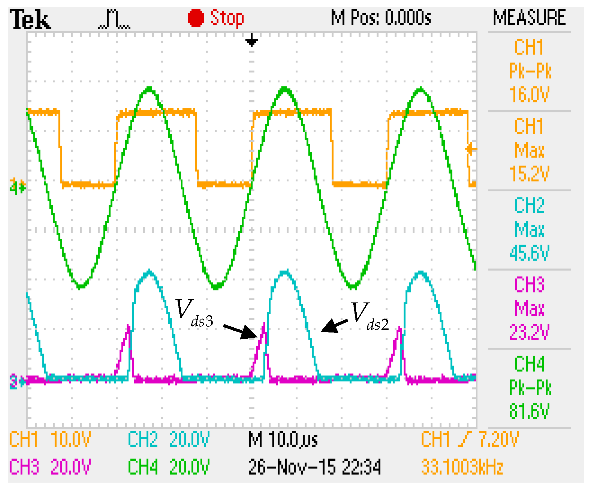
Figure 11 shows the waveforms of
VdS2,
VdS3 and
VCP from top to bottom. It can be seen that the synthesized waves of
VdS2 and
VdS3 are exactly half of the resonant wave
VCP on the condition of
D = 0.6. The same result can be detected that the synthesized waves of
VdS1 and
VdS4 are exactly half of the resonant wave
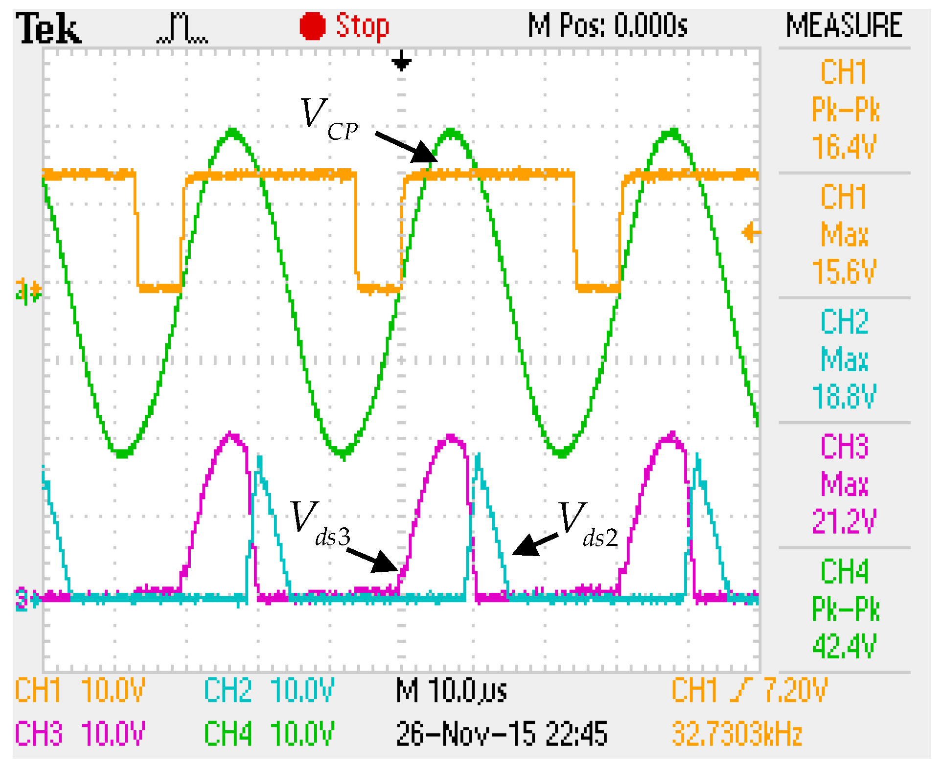
VCP. When the duty cycle becomes
D = 0.8, the waveforms of
VdS2,
VdS3 and
VCP are shown in
Figure 12 and
VdS2 and
VdS3 are changing when the duty cycle
D is changing.
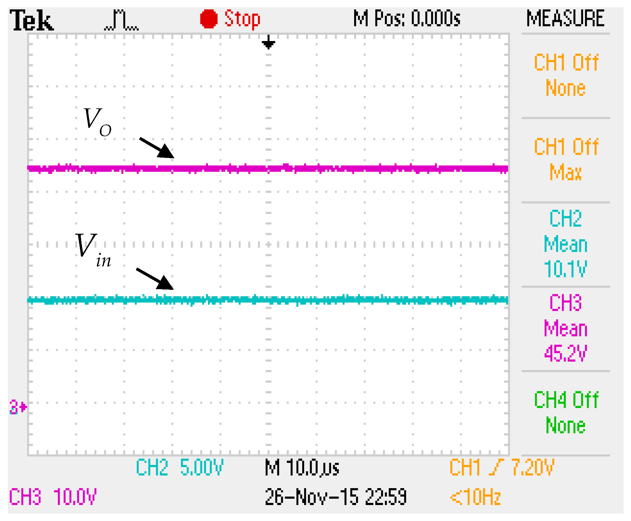
Figure 13 shows that
VO is controlled at 43 V for the condition of
R = 50 Ω and
D = 0.8, which achieves a gain of 4.3 times compared with the input voltage
Uin = 10 V. It verifies that the system can realize a higher gain by regulating the duty cycle
D.
Table 2 presents the experimental data of the proposed topology. The controlled gain range is from 1.6 to 7.3. With higher gain, the system can get higher output power. Furthermore, system efficiency can remain above 80%.
Figure 14 shows that the experimental results of voltage gain match with the theoretical results well, except that there is little difference at the maximum gain point. It is because power losses at the primary side will increase at the top gain point.
6. Discussion
In order to present a close loop control of the voltage gain, a Proportion Integration Differentiation (PID) control is applied to regulate the duty cycle
D of the switches. The close loop control structure can be shown in
Figure 15.
The information of output voltage VO is measured and sent back to the primary side by an Radio Frequency (RF)-link. Furthermore, a PID controller is utilized to control the duty cycle of S3 and S4, according to the difference between VO and Vref.
A load switching test was carried out to evaluate the controller’s performance. In this test, load condition is set to switching between 10 Ω and 30 Ω. The DC input voltage is set at 5 V. The output reference voltage is set at 20 V. The experimental result can be shown in
Figure 16.
As can be seen in
Figure 16, there are two load switching events in the control process: one is from 20 Ω to 10 Ω (first switching) and the other is from 10 Ω to 20 Ω (second switching). In the control process, the output voltage is kept stable except for some switching disturbance. The experimental results verify the close loop control performance of the PID controller.


