Thickness-Dependent Differential Reflectance Spectra of Monolayer and Few-Layer MoS2, MoSe2, WS2 and WSe2


 , , ,
, , , 

Abstract
:1. Introduction
2. Materials and Method
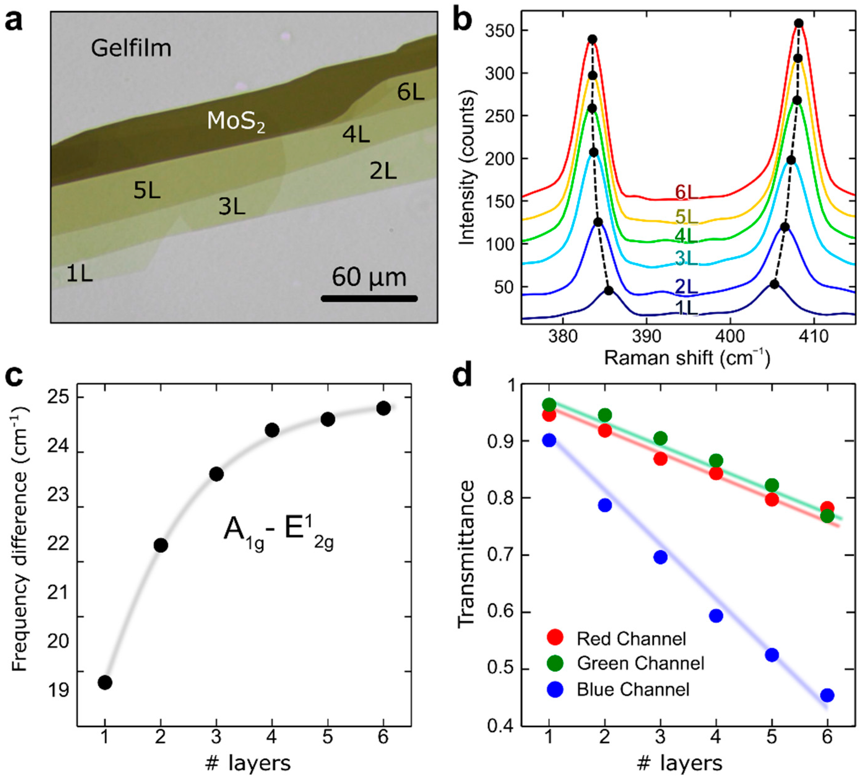
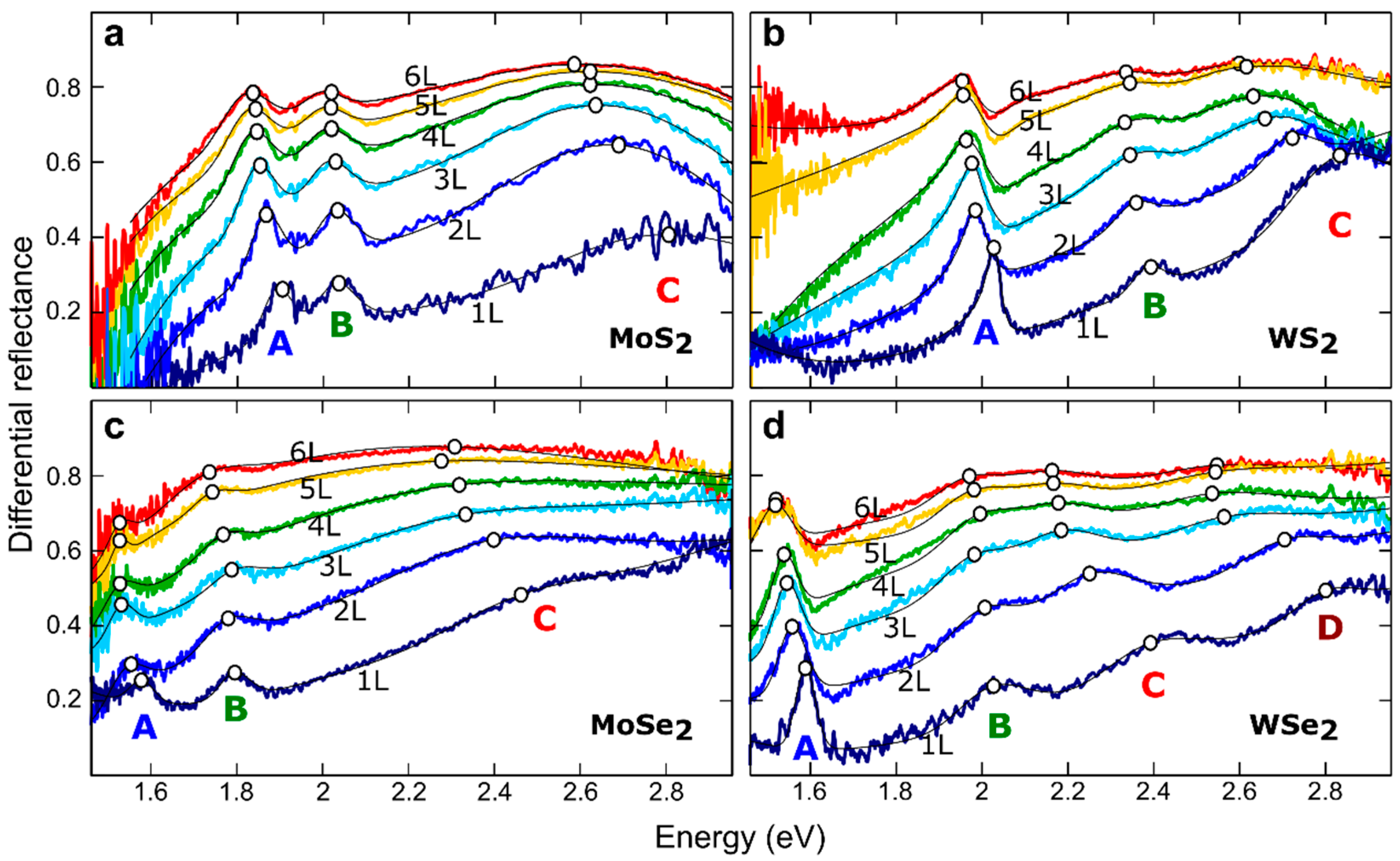
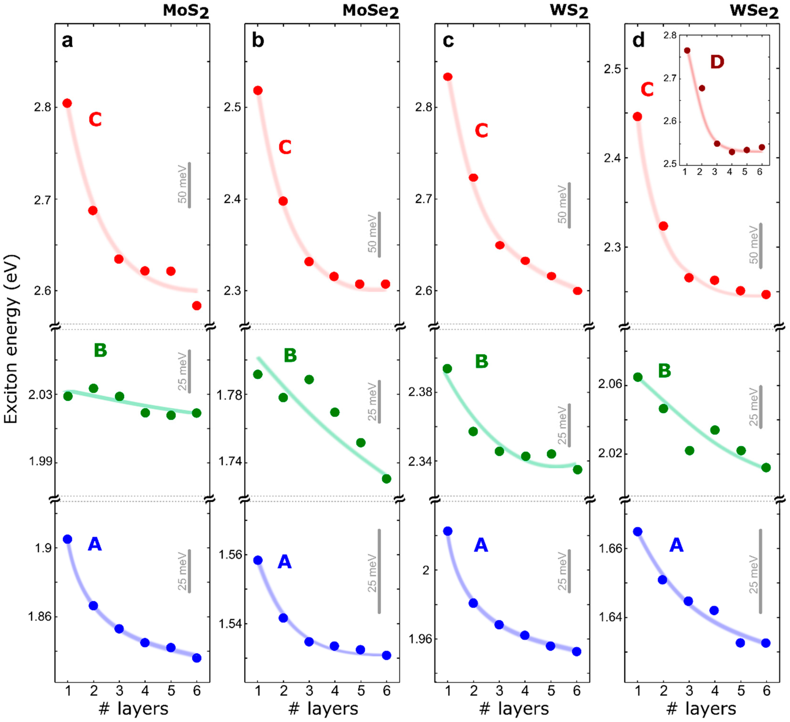
3. Results and Discussion
4. Conclusions
Supplementary Materials
Author Contributions
Funding
Acknowledgments
Conflicts of Interest
References
- Novoselov, K.S.; Jiang, D.; Schedin, F.; Booth, T.J.; Khotkevich, V.V.; Morozov, S.V.; Geim, A.K. Two-dimensional atomic crystals. Proc. Natl. Acad. Sci. USA 2005, 102, 10451–10453. [Google Scholar] [CrossRef] [PubMed] [Green Version]
- Xu, M.; Liang, T.; Shi, M.; Chen, H. Graphene-like two-dimensional materials. Chem. Rev. 2013, 113, 3766–3798. [Google Scholar] [CrossRef] [PubMed]
- Xia, F.; Wang, H.; Xiao, D.; Dubey, M.; Ramasubramaniam, A. Two-dimensional material nanophotonics. Nat. Photonics 2014, 8, 899–907. [Google Scholar] [CrossRef] [Green Version]
- Lv, R.; Robinson, J.A.; Schaak, R.E.; Sun, D.; Sun, Y.; Mallouk, T.E.; Terrones, M. Transition metal dichalcogenides and beyond: Synthesis, properties, and applications of single- and few-layer nanosheets. Acc. Chem. Res. 2015, 48, 56–64. [Google Scholar] [CrossRef] [PubMed]
- Wang, Q.H.; Kalantar-Zadeh, K.; Kis, A.; Coleman, J.N.; Strano, M.S. Electronics and optoelectronics of two-dimensional transition metal dichalcogenides. Nat. Nanotechnol. 2012, 7, 699–712. [Google Scholar] [CrossRef] [PubMed] [Green Version]
- Castellanos-Gomez, A. Why all the fuss about 2D semiconductors? Nat. Photonics 2016, 10, 202–204. [Google Scholar] [CrossRef] [Green Version]
- Avouris, P.; Xia, F. Graphene applications in electronics and photonics. MRS Bull. 2012, 37, 1225–1234. [Google Scholar] [CrossRef]
- Yin, Z.; Li, H.; Li, H.; Jiang, L.; Shi, Y.; Sun, Y.; Lu, G.; Zhang, Q.; Chen, X.; Zhang, H. Single-layer MoS2 phototransistors. ACS Nano 2012, 6, 74–80. [Google Scholar] [CrossRef] [PubMed]
- Lee, H.S.; Min, S.-W.; Chang, Y.-G.; Park, M.K.; Nam, T.; Kim, H.; Kim, J.H.; Ryu, S.; Im, S. MoS2 nanosheet phototransistors with thickness-modulated optical energy gap. Nano Lett. 2012, 12, 3695–3700. [Google Scholar] [CrossRef] [PubMed]
- Zhang, W.; Chiu, M.-H.; Chen, C.-H.; Chen, W.; Li, L.-J.; Wee, A.T.S. Role of metal contacts in high-performance phototransistors based on WSe2 monolayers. ACS Nano 2014, 8, 8653–8661. [Google Scholar] [CrossRef] [PubMed]
- Choi, W.; Cho, M.Y.; Konar, A.; Lee, J.H.; Cha, G.-B.; Hong, S.C.; Kim, S.; Kim, J.; Jena, D.; Joo, J.; et al. High-detectivity multilayer MoS2 phototransistors with spectral response from ultraviolet to infrared. Adv. Mater. 2012, 24, 5832–5836. [Google Scholar] [CrossRef] [PubMed]
- Zhang, W.; Huang, J.-K.; Chen, C.-H.; Chang, Y.-H.; Cheng, Y.-J.; Li, L.-J. High-gain phototransistors based on a CVD MoS₂ monolayer. Adv. Mater. 2013, 25, 3456–3461. [Google Scholar] [CrossRef] [PubMed]
- Abderrahmane, A.; Ko, P.J.; Thu, T.V.; Ishizawa, S.; Takamura, T.; Sandhu, A. High photosensitivity few-layered MoSe2 back-gated field-effect phototransistors. Nanotechnology 2014, 25, 365202. [Google Scholar] [CrossRef] [PubMed]
- Lopez-Sanchez, O.; Lembke, D.; Kayci, M.; Radenovic, A.; Kis, A. Ultrasensitive photodetectors based on monolayer MoS2. Nat. Nanotechnol. 2013, 8, 497–501. [Google Scholar] [CrossRef] [PubMed]
- Ross, J.S.; Klement, P.; Jones, A.M.; Ghimire, N.J.; Yan, J.; Mandrus, D.G.; Taniguchi, T.; Watanabe, K.; Kitamura, K.; Yao, W.; et al. Electrically tunable excitonic light-emitting diodes based on monolayer WSe2 p-n junctions. Nat. Nanotechnol. 2014, 9, 268–272. [Google Scholar] [CrossRef] [PubMed]
- Baugher, B.W.H.; Churchill, H.O.H.; Yang, Y.; Jarillo-Herrero, P. Optoelectronic devices based on electrically tunable p-n diodes in a monolayer dichalcogenide. Nat. Nanotechnol. 2014, 9, 262–267. [Google Scholar] [CrossRef] [PubMed]
- Pospischil, A.; Furchi, M.M.; Mueller, T. Solar-energy conversion and light emission in an atomic monolayer p-n diode. Nat. Nanotechnol. 2014, 9, 257–261. [Google Scholar] [CrossRef] [PubMed]
- Lee, C.-H.; Lee, G.-H.; van der Zande, A.M.; Chen, W.; Li, Y.; Han, M.; Cui, X.; Arefe, G.; Nuckolls, C.; Heinz, T.F.; et al. Atomically thin p–n junctions with van der Waals heterointerfaces. Nat. Nanotechnol. 2014, 9, 676–681. [Google Scholar] [CrossRef] [PubMed] [Green Version]
- Groenendijk, D.J.; Buscema, M.; Steele, G.A.; Michaelis de Vasconcellos, S.; Bratschitsch, R.; van der Zant, H.S.J.; Castellanos-Gomez, A. Photovoltaic and photothermoelectric effect in a double-gated WSe2 device. Nano Lett. 2014, 14, 5846–5852. [Google Scholar] [CrossRef] [PubMed]
- Splendiani, A.; Sun, L.; Zhang, Y.; Li, T.; Kim, J.; Chim, C.-Y.; Galli, G.; Wang, F. Emerging photoluminescence in monolayer MoS2. Nano Lett. 2010, 10, 1271–1275. [Google Scholar] [CrossRef] [PubMed]
- Mak, K.F.; Lee, C.; Hone, J.; Shan, J.; Heinz, T.F. Atomically Thin MoS2: A new direct-gap semiconductor. Phys. Rev. Lett. 2010, 105, 136805. [Google Scholar] [CrossRef] [PubMed]
- Zhao, W.; Ghorannevis, Z.; Chu, L.; Toh, M.; Kloc, C.; Tan, P.-H.; Eda, G. Evolution of electronic structure in atomically thin sheets of WS2 and WSe2. ACS Nano 2013, 7, 791–797. [Google Scholar] [CrossRef] [PubMed]
- Li, Y.; Li, X.; Yu, T.; Yang, G.; Chen, H.; Zhang, C.; Feng, Q.; Ma, J.; Liu, W.; Xu, H. Accurate identification of layer number for few-layer WS2 and WSe2 via spectroscopic study. Nanotechnology 2018, 29, 124001. [Google Scholar] [CrossRef] [PubMed]
- Ottaviano, L.; Palleschi, S.; Perrozzi, F.; D’Olimpio, G.; Priante, F.; Donarelli, M.; Benassi, P.; Nardone, M.; Gonchigsuren, M.; Gombosuren, M. Mechanical exfoliation and layer number identification of MoS2 revisited. 2D Mater. 2017, 4, 45013. [Google Scholar] [CrossRef]
- Li, D.; Song, X.; Xu, J.; Wang, Z.; Zhang, R.; Zhou, P.; Zhang, H.; Huang, R.; Wang, S.; Zheng, Y. Optical properties of thickness-controlled MoS2 thin films studied by spectroscopic ellipsometry. Appl. Surf. Sci. 2017, 421, 884–890. [Google Scholar] [CrossRef]
- Dhakal, K.P.; Duong, D.L.; Lee, J.; Nam, H.; Kim, M.; Kan, M.; Lee, Y.H.; Kim, J. Confocal absorption spectral imaging of MoS2: Optical transitions depending on the atomic thickness of intrinsic and chemically doped MoS2. Nanoscale 2014, 6, 13028–13035. [Google Scholar] [CrossRef] [PubMed]
- Castellanos-Gomez, A.; Quereda, J.; van der Meulen, H.P.; Agraït, N.; Rubio-Bollinger, G. Spatially resolved optical absorption spectroscopy of single- and few-layer MoS2 by hyperspectral imaging. Nanotechnology 2016, 27, 115705. [Google Scholar] [CrossRef] [PubMed]
- Frisenda, R.; Niu, Y.; Gant, P.; Molina-Mendoza, A.J.; Schmidt, R.; Bratschitsch, R.; Liu, J.; Fu, L.; Dumcenco, D.; Kis, A.; et al. Micro-reflectance and transmittance spectroscopy: A versatile and powerful tool to characterize 2D materials. J. Phys. D Appl. Phys. 2017, 50, 74002. [Google Scholar] [CrossRef]
- Rohlfing, M. Electronic excitations from a perturbative LDA + GdW approach. Phys. Rev. B 2010, 82, 205127. [Google Scholar] [CrossRef]
- Böker, T.; Severin, R.; Müller, A.; Janowitz, C.; Manzke, R.; Voß, D.; Krüger, P.; Mazur, A.; Pollmann, J. Band structure of MoS2, MoSe2, and α-MoTe2: Angle-resolved photoelectron spectroscopy and ab initio calculations. Phys. Rev. B 2001, 64, 235305. [Google Scholar] [CrossRef]
- Yun, W.S.; Han, S.W.; Hong, S.C.; Kim, I.G.; Lee, J.D. Thickness and strain effects on electronic structures of transition metal dichalcogenides: 2H-MX2 semiconductors (M = Mo, W; X = S, Se, Te). Phys. Rev. B 2012, 85, 33305. [Google Scholar] [CrossRef]
- Buscema, M.; Steele, G.A.; van der Zant, H.S.J.; Castellanos-Gomez, A. The effect of the substrate on the Raman and photoluminescence emission of single-layer MoS2. Nano Res. 2014, 7, 561–571. [Google Scholar] [CrossRef]
- Lee, C.; Yan, H.; Brus, L.E.; Heinz, T.F.; Hone, Ќ.J.; Ryu, S. Anomalous Lattice Vibrations of Single-and Few-Layer MoS2. ACS Nano 2010, 4, 2695–2700. [Google Scholar] [CrossRef] [PubMed]
- Placidi, M.; Dimitrievska, M.; Izquierdo-Roca, V.; Fontané, X.; Castellanos-Gomez, A.; Pérez-Tomás, A.; Mestres, N.; Espindola-Rodriguez, M.; López-Marino, S.; Neuschitzer, M. Multiwavelength excitation Raman scattering analysis of bulk and two-dimensional MoS2: Vibrational properties of atomically thin MoS2 layers. 2D Mater. 2015, 2, 35006. [Google Scholar] [CrossRef]
- Zhang, H.; Ran, F.; Shi, X.; Fang, X.; Wu, S.; Liu, Y.; Zheng, X.; Yang, P.; Liu, Y.; Wang, L.; et al. Optical thickness identification of transition metal dichalcogenide nanosheets on transparent substrates. Nanotechnology 2017, 28, 164001. [Google Scholar] [CrossRef] [PubMed]
- Castellanos-Gomez, A.; Roldán, R.; Cappelluti, E.; Buscema, M.; Guinea, F.; van der Zant, H.S.J.; Steele, G.A. Local strain engineering in atomically thin MoS2. Nano Lett. 2013, 13, 5361–5366. [Google Scholar] [CrossRef] [PubMed]
- Plechinger, G.; Heydrich, S.; Eroms, J.; Weiss, D.; Schüller, C.; Korn, T. Raman spectroscopy of the interlayer shear mode in few-layer MoS2 flakes. Appl. Phys. Lett. 2012, 101, 101906. [Google Scholar] [CrossRef]
- Zhao, W.; Ghorannevis, Z.; Amara, K.K.; Pang, J.R.; Toh, M.; Zhang, X.; Kloc, C.; Tan, P.H.; Eda, G. Lattice dynamics in mono-and few-layer sheets of WS2 and WSe2. Nanoscale 2013, 5, 9677–9683. [Google Scholar] [CrossRef] [PubMed]
- Zhang, X.; Han, W.P.; Wu, J.B.; Milana, S.; Lu, Y.; Li, Q.Q.; Ferrari, A.C.; Tan, P.H. Raman spectroscopy of shear and layer breathing modes in multilayer MoS2. Phys. Rev. B 2013, 87, 115413. [Google Scholar] [CrossRef]
- Zhao, Y.; Luo, X.; Li, H.; Zhang, J.; Araujo, P.T.; Gan, C.K.; Wu, J.; Zhang, H.; Quek, S.Y.; Dresselhaus, M.S. Interlayer breathing and shear modes in few-trilayer MoS2 and WSe2. Nano Lett. 2013, 13, 1007–1015. [Google Scholar] [CrossRef] [PubMed]
- Tonndorf, P.; Schmidt, R.; Böttger, P.; Zhang, X.; Börner, J.; Liebig, A.; Albrecht, M.; Kloc, C.; Gordan, O.; Zahn, D.R.T.; et al. Photoluminescence emission and Raman response of monolayer MoS2, MoSe2, and WSe2. Opt. Express 2013, 21, 4908. [Google Scholar] [CrossRef] [PubMed]
- Puretzky, A.A.; Liang, L.; Li, X.; Xiao, K.; Wang, K.; Mahjouri-Samani, M.; Basile, L.; Idrobo, J.C.; Sumpter, B.G.; Meunier, V. Low-frequency Raman fingerprints of two-dimensional metal dichalcogenide layer stacking configurations. ACS Nano 2015, 9, 6333–6342. [Google Scholar] [CrossRef] [PubMed]
- Ghasemi, F.; Frisenda, R.; Dumcenco, D.; Kis, A.; Perez de Lara, D.; Castellanos-Gomez, A. High Throughput Characterization of Epitaxially Grown Single-Layer MoS2. Electronics 2017, 6, 28. [Google Scholar] [CrossRef]
- McIntyre, J.D.E.; Aspnes, D.E. Differential reflection spectroscopy of very thin surface films. Surf. Sci. 1971, 24, 417–434. [Google Scholar] [CrossRef]
- Qiu, D.Y.; da Jornada, F.H.; Louie, S.G. Optical Spectrum of MoS2: Many-body effects and diversity of exciton states. Phys. Rev. Lett. 2013, 111, 216805. [Google Scholar] [CrossRef] [PubMed]
- Kozawa, D.; Kumar, R.; Carvalho, A.; Kumar Amara, K.; Zhao, W.; Wang, S.; Toh, M.; Ribeiro, R.M.; Castro Neto, A.H.; Matsuda, K.; et al. Photocarrier relaxation pathway in two-dimensional semiconducting transition metal dichalcogenides. Nat. Commun. 2014, 5, 193–335. [Google Scholar] [CrossRef] [PubMed]
- Klots, A.R.; Newaz, A.K.M.; Wang, B.; Prasai, D.; Krzyzanowska, H.; Lin, J.; Caudel, D.; Ghimire, N.J.; Yan, J.; Ivanov, B.L.; et al. Probing excitonic states in suspended two-dimensional semiconductors by photocurrent spectroscopy. Sci. Rep. 2014, 4, 6608. [Google Scholar] [CrossRef] [PubMed] [Green Version]
- Gibaja, C.; Rodriguez-San-Miguel, D.; Ares, P.; Gómez-Herrero, J.; Varela, M.; Gillen, R.; Maultzsch, J.; Hauke, F.; Hirsch, A.; Abellán, G.; et al. Few-layer antimonene by liquid-phase exfoliation. Angew. Chem. Int. Ed. 2016. [Google Scholar] [CrossRef]
- Schmidt, R.; Niehues, I.; Schneider, R.; Drüppel, M.; Deilmann, T.; Rohlfing, M.; de Vasconcellos, S.M.; Castellanos-Gomez, A.; Bratschitsch, R. Reversible uniaxial strain tuning in atomically thin WSe2. 2D Mater. 2016, 3, 21011. [Google Scholar] [CrossRef]
- Frisenda, R.; Drüppel, M.; Schmidt, R.; Michaelis de Vasconcellos, S.; Perez de Lara, D.; Bratschitsch, R.; Rohlfing, M.; Castellanos-Gomez, A. Biaxial strain tuning of the optical properties of single-layer transition metal dichalcogenides. NPJ 2D Mater. Appl. 2017, 1, 10. [Google Scholar] [CrossRef]
- Arora, A.; Koperski, M.; Nogajewski, K.; Marcus, J.; Faugeras, C.; Potemski, M. Excitonic resonances in thin films of WSe2: From monolayer to bulk material. Nanoscale 2015, 7, 10421–10429. [Google Scholar] [CrossRef] [PubMed]


| Material | Experimental A-B Splitting (meV) | Theoretical A-B Splitting (meV) |
|---|---|---|
| 1L—MoS2 | 124 ± 5 | 152 |
| 1L—MoSe2 | 219 ± 10 | 218 |
| 1L—WS2 | 371 ± 5 | 420 |
| 1L—WSe2 | 398 ± 10 | 464 |
© 2018 by the authors. Licensee MDPI, Basel, Switzerland. This article is an open access article distributed under the terms and conditions of the Creative Commons Attribution (CC BY) license (http://creativecommons.org/licenses/by/4.0/).
Share and Cite
Niu, Y.; Gonzalez-Abad, S.; Frisenda, R.; Marauhn, P.; Drüppel, M.; Gant, P.; Schmidt, R.; Taghavi, N.S.; Barcons, D.; Molina-Mendoza, A.J.; et al. Thickness-Dependent Differential Reflectance Spectra of Monolayer and Few-Layer MoS2, MoSe2, WS2 and WSe2. Nanomaterials 2018, 8, 725. https://doi.org/10.3390/nano8090725
Niu Y, Gonzalez-Abad S, Frisenda R, Marauhn P, Drüppel M, Gant P, Schmidt R, Taghavi NS, Barcons D, Molina-Mendoza AJ, et al. Thickness-Dependent Differential Reflectance Spectra of Monolayer and Few-Layer MoS2, MoSe2, WS2 and WSe2. Nanomaterials. 2018; 8(9):725. https://doi.org/10.3390/nano8090725
Chicago/Turabian StyleNiu, Yue, Sergio Gonzalez-Abad, Riccardo Frisenda, Philipp Marauhn, Matthias Drüppel, Patricia Gant, Robert Schmidt, Najme S. Taghavi, David Barcons, Aday J. Molina-Mendoza, and et al. 2018. "Thickness-Dependent Differential Reflectance Spectra of Monolayer and Few-Layer MoS2, MoSe2, WS2 and WSe2" Nanomaterials 8, no. 9: 725. https://doi.org/10.3390/nano8090725
APA StyleNiu, Y., Gonzalez-Abad, S., Frisenda, R., Marauhn, P., Drüppel, M., Gant, P., Schmidt, R., Taghavi, N. S., Barcons, D., Molina-Mendoza, A. J., De Vasconcellos, S. M., Bratschitsch, R., Perez De Lara, D., Rohlfing, M., & Castellanos-Gomez, A. (2018). Thickness-Dependent Differential Reflectance Spectra of Monolayer and Few-Layer MoS2, MoSe2, WS2 and WSe2. Nanomaterials, 8(9), 725. https://doi.org/10.3390/nano8090725