3.3. Chemical Composition
The chemical composition was investigated by XPS. The scans were taken before and after Ar sputter-cleaning of the substrate to investigate the extent of surface contamination.
Table 2 shows the analysis of survey scans of the deposited material for the unsputtered samples while
Table 3 shows the relative concentrations of Cu and Cl after Ar sputter cleaning for 150 s. The XPS analysis was not performed in situ so there will be significant amounts of adventitious carbon from environmental contamination between deposition and analysis for the unsputtered films. The sputtered samples show significantly reduced C 1
s signal. There is evidence, however, of the presence of carbon as a residue from the organic precursors (see below). There is also some fluorine content in all films which must come from the CuBTMSA precursor. There is significant uncertainty in the Cu/Cl ration due to the dispersed crystallites which allow a large signal from the substrate material to be detected and because the relative sensitivity factor for the XPS quantification for the Cl 2
p peak is much lower than for the Cu 2
p peaks by a factor of ~11. Nevertheless, for the unsputtered samples the Cu/Cl ratio is lower than the expected 1/1 ratio for CuCl; however, the sputter-cleaned samples show close to the stoichiometric ratio. The low CuCl ratio for the unsputtered samples arises from the different composition of the surface layer.
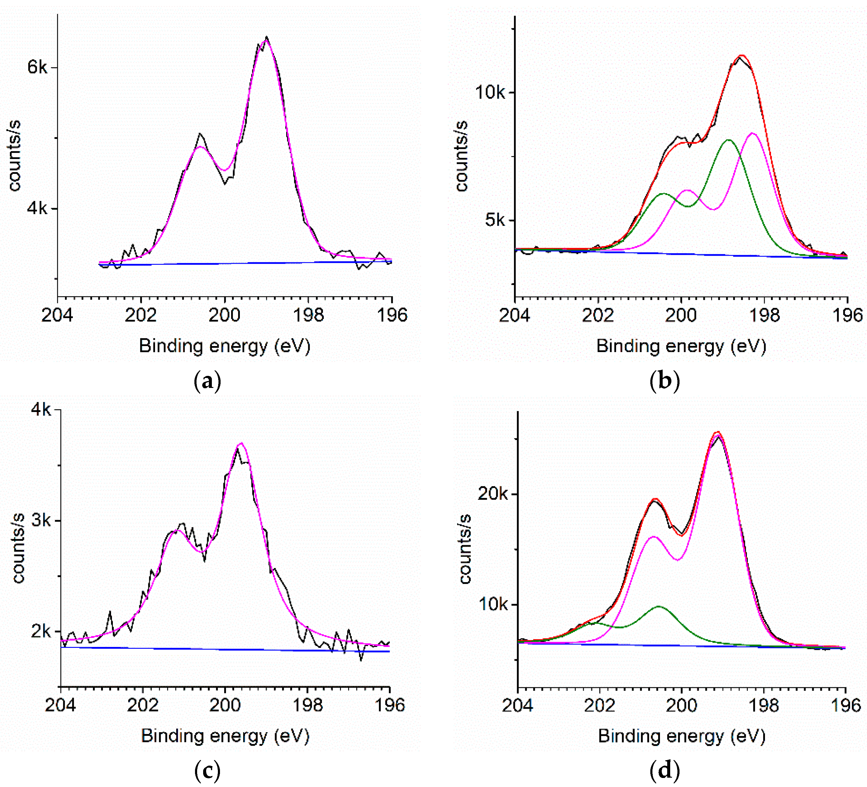
High-resolution scans of the Cl 2
p peak from the uncapped samples with peak fittings are shown in
Figure 4 for the unsputtered and sputter-cleaned samples. For Q1, Q5, and Q7 the Cl 2
p peak is well fitted by one 2
p doublet consisting of 2
p3/2 and 2
p1/2 components separated by 1.6 eV.
Figure 4a is representative of these. The binding energy values are consistent with those given for copper chlorides although they cannot easily distinguish between Cu(I) and Cu(II) chloride. In general, the CuCl
2 should appear at a higher binding energy [
24,
25,
26]. Taking into account the XRD results which show only CuCl we conclude that peak at ~199.0 eV is CuCl. There is no significant ClO
x formation: this would give rise to 2
p3/2 peaks at energies approximately 206–208 eV [
27], and there is no evidence of these in the Cl 2
p spectra. The peak details are given in
Table 4. For sample Q10, if a single peak fitting is used, the fitting error is significantly higher. However, the measured Q10 signal can be well fitted with two 2
p components separated by 0.6 eV (
Figure 4b). This is consistent with the emergence of two different bonding environments for Cl. The lower energy peak is characteristic of HCl·
nH
2O (198.4 eV) [
28] and is also consistent with CuCl bound to an organic ligand [
29]. The peak area ratio between this component and the one at slightly lower energy is 1.4 indicating significant surface contamination.
Figure 4c shows the Cl 2
p peak for Q7 after Ar sputter-cleaning. For the Ar-sputtered Q10 sample, again the best fit is with two doublets. In this case, the additional peak appears at higher energy, consistent with the existence of an organic chloride [
28,
30].
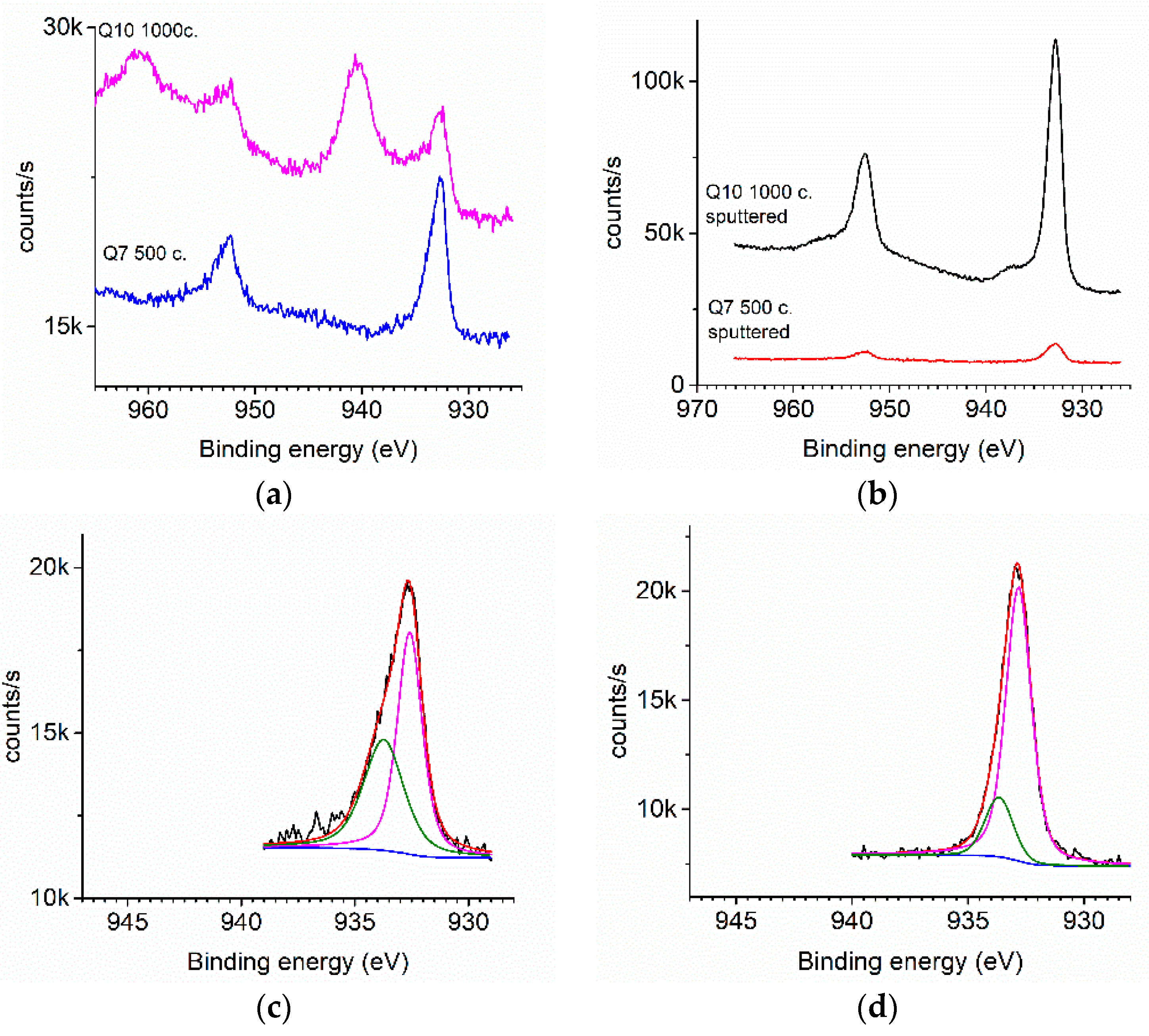
Figure 5 shows the high resolution 2
p3/2 and 2
p1/2 raw data scans scan of Cu and the decomposition of the 2
p3/2 peaks into individual components. Q7 is representative of the other samples with less than 1000 c. deposition.
Table 5 shows the peak positions and full width half maxima (FWHM).
It is difficult to separate the Cu
0, Cu
+, and Cu
2+ peaks solely by their binding energies but taking into account the XRD spectra, peak P1 is assigned to CuCl which has been previously seen at 932.4–932.6 eV [
31,
32]. Peak P2 (~934 eV) could be indicative of CuO, CuCl
2, or Cu with an organic or organo-chlorate ligand [
33,
34,
35,
36]. However, the presence of Cu
2+ species should be indicated by an obvious shake-up satellite peak at ~940 eV [
37] and there is no evidence of this in Q7 both with and without sputtering (
Figure 5a,b). Neither is there evidence for chlorate bonding in the Cl 2
p spectra. Therefore, Q7 contains only Cu
+ bonds and P2 is ascribed to Cu(I) organic bonding. The amount of the Cu organic contamination in both Q7 and Q10 is clearly less after Ar sputtering (
Figure 5d,f).
Figure 5a,e, Q10 (1000 c., unsputtered), shows a large satellite peak at the expected energy for Cu
2+ at ~940 eV together with a peak at 936.7 eV, P3, which may be evidence for some fluoride bound to organic material [
38]. However, the Q10 Ar-sputtered sample,
Figure 5f, shows the same three peaks as for the Q10 unsputtered sample with no evidence of a satellite peak. Therefore, it is not clear which of the peaks is related to the Cu
2+ satellite peak. It may be that the relatively lower intensity of P3 after Ar sputtering gives rise to a much smaller satellite peak which is not visible in
Figure 5f.
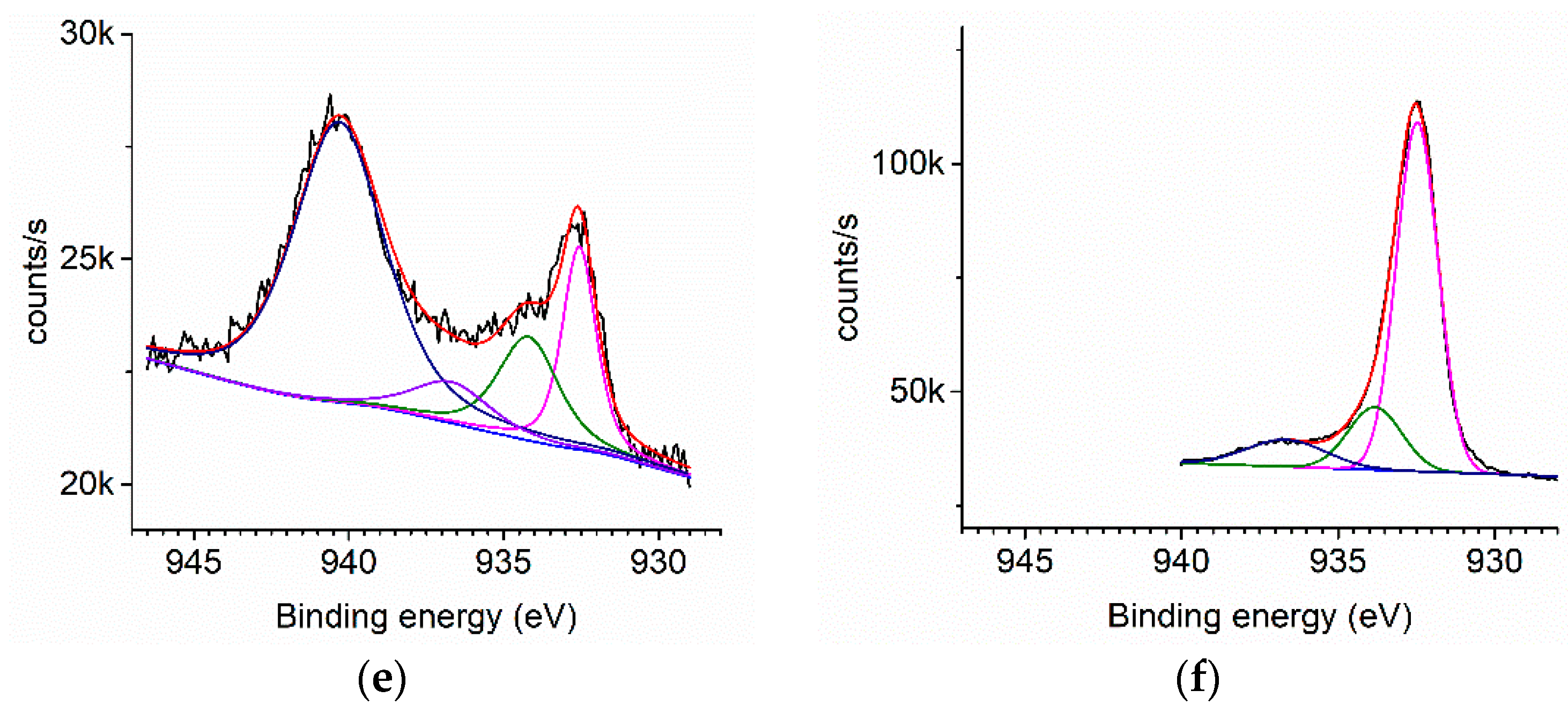
Observation of the O 1
s spectra yields further information. The spectra for Q7 and Q10 before and for Q10 after Ar sputtering are shown in
Figure 6. The samples are dominated by the peak at 533.3 eV due to SiO
2 [
39] from the quartz since the substrate coverage is not complete. Both unsputtered samples,
Figure 6a,b, also show a peak at ~534 eV which is probably O in an organic ligand indicating some residual CuBTMSA precursor material in the film. In addition,
Figure 6b shows a large additional peak at 535.8 eV, which is at an energy which has been ascribed to an O atom linked to a CF containing ligand [
30]. This again is likely due to some partially decomposed CuBTMSA precursor.
Figure 6c is representative of all the sputtered samples and shows only the SiO
2 peak indicating that the oxygen bonded to organic material is only on the surface.
When the Cl 2p, Cu 2p, and O 1s results are taken together with the XRD results, it is clear that the bulk of the films consists of γ-CuCl with a certain amount of organic contamination from the precursor molecules. This is confirmed by the presence of significant carbon content even in the Ar-sputtered samples. The unsputtered samples show, as is to be expected, greater organic contamination, including from F-containing organic fragments and HCl from the CuBTMSA and PyrHCl precursors, respectively. The exact nature of the bonding is the subject of further investigation.
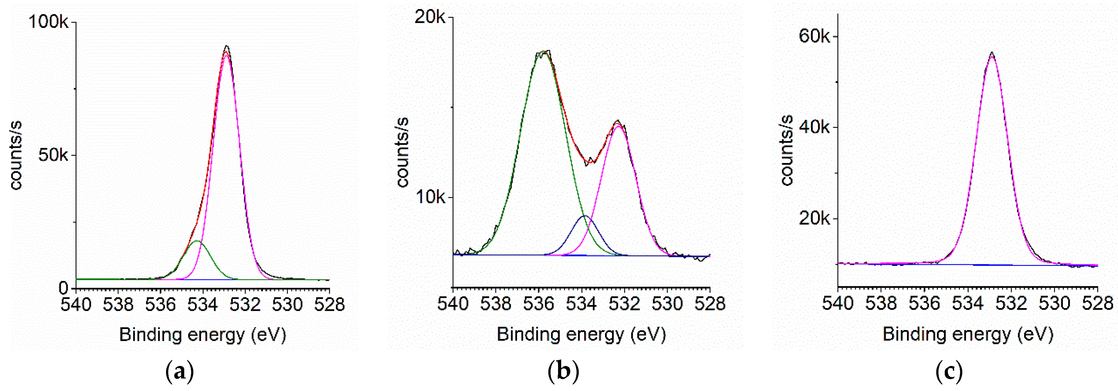
Thin uncapped CuCl films will hydrolyse after approximately one day.
Figure 7 and
Table 3,
Table 4 and
Table 5 show measurements on the sputter cleaned sample Q8 (500 c., Al
2O
3 capped) after exposure to normal atmosphere for approximately 3 weeks. The curves and tabulated data are very similar to those of the uncapped samples with the same number of growth cycles kept in an inert atmosphere (
Figure 4c and
Figure 5e). They show no evidence of degradation, indicating that 5 nm of oxide capping layer provides an effective barrier to hydrolysis of the films.
3.4. Photoluminescence
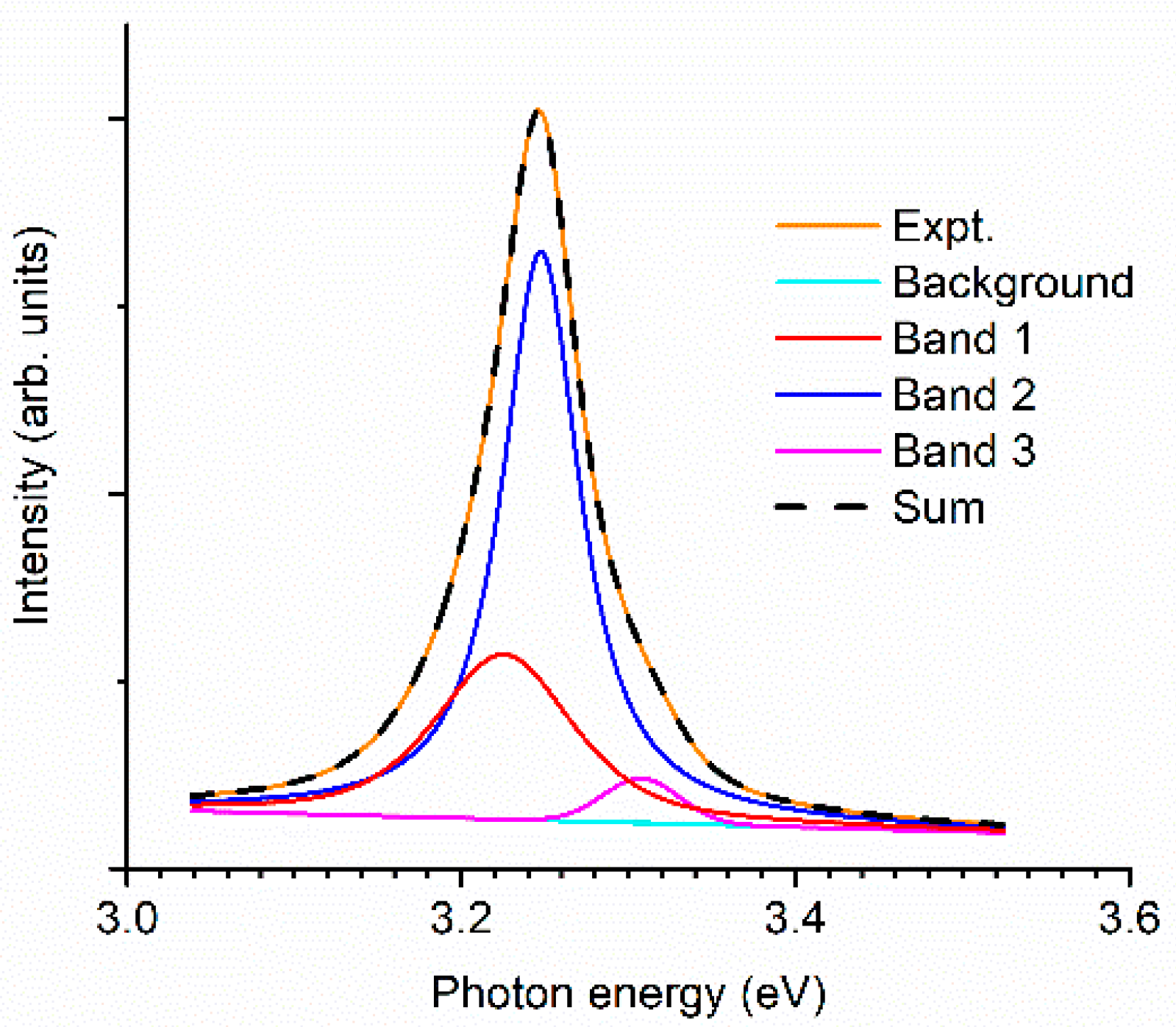
The photoluminescence signals obtained from sample Q10 (1000 c., uncapped) were easily measurable at room temperature. Shown in
Figure 8 is the experimental spectrum, decomposed into three Gaussian bands located on a linear background. The sum fits the measured data within background noise. The band parameters are listed in
Table 6. We use band area as the measure of its strength. The location of the PL maximum is very close to the position of the strongest PL2 band, coinciding with the position of the absorption peak PL2 (3.248 eV) of
Table 6 within experimental uncertainty. The weaker but discernible high-energy PL3 band at 3.308 eV lies 0.06 eV above PL2. The lower energy band PL1 is situated at 3.225 eV, approximately 0.10 eV lower than PL2. These results are similar to those observed on CuCl films obtained by thermal evaporation [
40] and magnetron sputtering [
41]. Those showed that at low temperature the emission peak could be resolved into three components which broadened into one composite peak at room temperature. The main peak was identified as the
Z3 free exciton peak observed at energy 3.227 eV at 15 K. This peak shifted to higher energy of 3.243 eV at room temperature, a shift of approximately 0.016 eV [
42]. This peak is almost at the same energy as the main peak reported here (3.248 eV). The peak shown here can also be decomposed into three components. By comparison with these results and allowing for the shift with temperature, the main peak indicating the most probable radiative channel is ascribed to the
Z3 exciton. The lower energy peak we see at 3.225 eV (385.4 nm) can be ascribed to the
I1 peak due to an exciton bound to an impurity, probably a Cu vacancy [
43]. The higher energy peak at 3.308 eV (375.8 nm) can be ascribed to the
Z1,2 exciton. PL mapping across the sample shown in
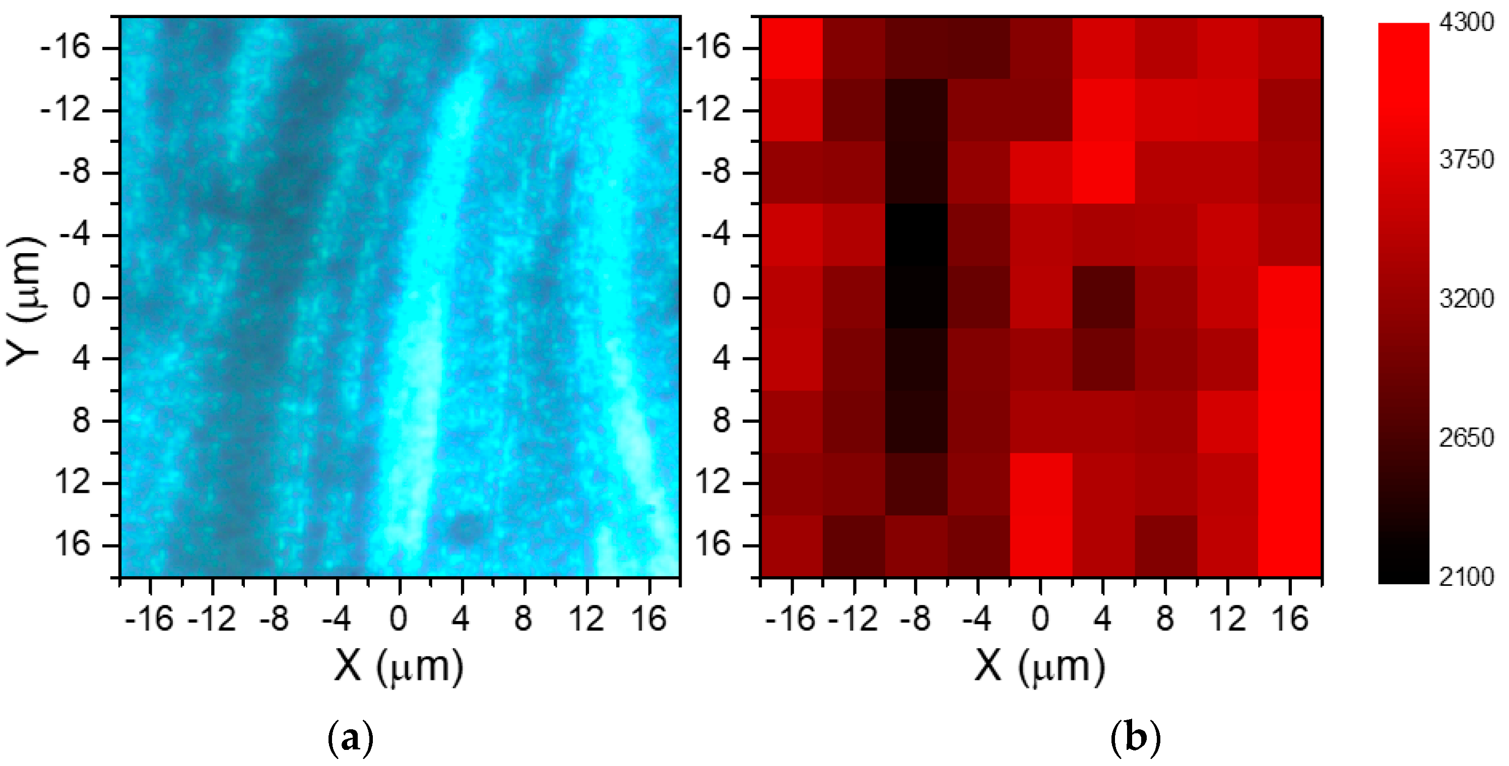
Figure 9 (32 × 32 μm
2, step 4 μm) shows intensity varying by a factor of approximately 2, due to local variations of the effective film thickness. No changes in peak position, width or shape were observed.
3.5. Reflectance
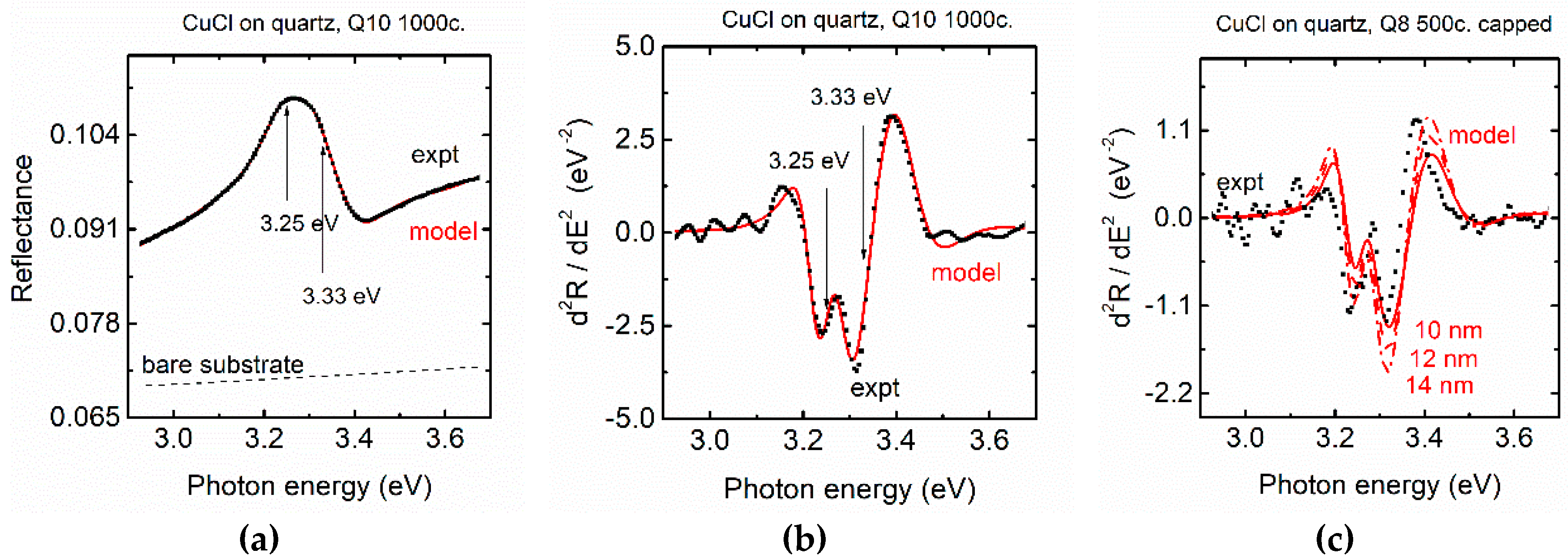
The measured reflectance spectrum of the thickest uncapped CuCl film (Q10 1000 c.) is shown in
Figure 10a. It shows a significant increase of the reflected intensity compared to the bare substrate, which is indicative of a larger optical density of the film. In addition, a fairly strong spectral structure with maximum intensity at about 3.3 eV has apparently at least two narrow components. The latter are better seen in the twice differentiated spectra plotted in
Figure 10b. The differentiation enhances the sharper structures and suppresses the flat background. Based on the narrow structures in the derivative spectra, we have fitted the measured reflectance with a model consisting of a flat background dielectric function, with two superposed Gaussian absorption bands. The model lineshape of
Figure 10a,b represents the best-fit results with the (fitted) value of the film thickness of 29 nm, and the background value of the real part of its dielectric function of 3.2. The resulting parameters of the bands are listed in
Table 7. The strength parameter is proportional to the area below the absorptive (imaginary) part of the dielectric function, having the units of eV; however, we are interested in relative values and use arbitrary units here.
The two Gaussian bands are 0.08 eV apart, which is in a good agreement with the distance of 0.06 eV seen in the absorption spectra of
Z3 (3.23 eV) and
Z1,2 (3.308 eV) excitons at in the PL results and those seen at 4 K [
44]. In addition, the significantly larger strength of the upper (3.30 eV) band is clearly seen in the reflectance results, in contrast to the PL intensities. This is similar to the relative intensities seen in direct optical absorption measurements [
18,
45]. We have also observed a weak and broad luminescence band centred at about 2.7 eV, with the maximum signal below 4% of the main PL band; its high energy tail forms the smooth background seen in
Figure 7. This may be due to radiative recombination of defect states in the CuCl crystallites, as well as other species present in the deposited layer.
A film of the sample Q8 (500 c. with an Al
2O
3 capping layer) displays a reduced intensity excitonic structure in the differentiated reflectance, see
Figure 10c. The results are compatible with reduced effective film thickness of approximately 12 nm. In addition, the upper lineshape seems to be narrower than that of the thicker sample Q10, probably due to the smaller dispersion of the crystallite sizes. It can be seen that reflectance measurements are a useful way to identify the presence of CuCl in thin films. This method would be particularly useful where the film is deposited on a non-UV transparent substrate.
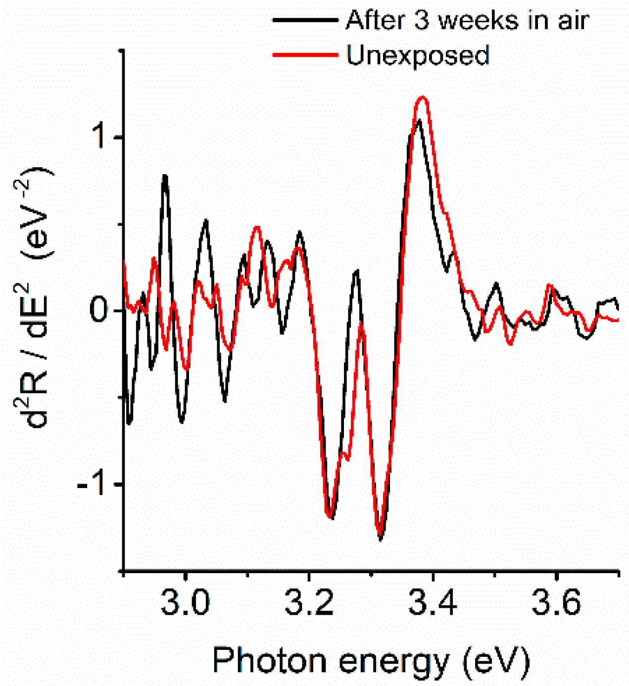
The reflectance of sample Q8 was remeasured after approximately three weeks in normal atmosphere. A comparison between the two measurements is shown in
Figure 11. There is no significant change to the excitonic absorption confirming the XPS results that 5 nm of ALD Al
2O
3 provides an effective protection layer for the CuCl. This is consistent with published work showing that ALD Al
2O
3 constitutes a good moisture diffusion barrier when applied to other materials [
46].


 ,
, 


