Next Issue
Volume 14, September
Previous Issue
Volume 14, March


J. Low Power Electron. Appl., Volume 14, Issue 2 (June 2024) – 16 articles

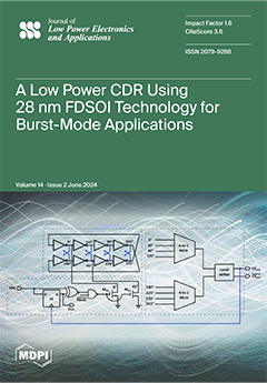
Cover Story (view full-size image): In this paper, we present a low-power Injection-Locked Clock and Data Recovery (ILCDR) circuit using 28nm FDSOI technology. The back-gate auto-biasing of FDSOI transistors allows for a compact Quadrature Ring Oscillator (QRO) that is smaller and has reduced levels of power consumption compared to an LC tank oscillator. By injecting a digital signal, we achieve an Injection-Locked Oscillator (ILO) with a low jitter. This leads to a low power ILCDR with a fast locking time and low jitter for burst-mode applications. The key innovation is a complementary QRO using back-gate control with FDSOI technology, resulting in an efficient ILCDR circuit. Post-layout simulations show a recovered clock jitter of 26.7ps and a data jitter of 11.9ps with a power consumption of 318μW at 0.6V. The estimated chip area is around 6600 μm². View this paper
  • Issues are regarded as officially published after their release is announced to the table of contents alert mailing list.
  • You may sign up for e-mail alerts to receive table of contents of newly released issues.
  • PDF is the official format for papers published in both, html and pdf forms. To view the papers in pdf format, click on the "PDF Full-text" link, and use the free Adobe Reader to open them.
Order results
Result details
Select all
Export citation of selected articles as:
18 pages, 6129 KiB  
Article
OptimalNN: A Neural Network Architecture to Monitor Chemical Contamination in Cancer Alley
by Uchechukwu Leo Udeji and Martin Margala
J. Low Power Electron. Appl. 2024, 14(2), 33; https://doi.org/10.3390/jlpea14020033 - 10 Jun 2024
Viewed by 1676
Abstract
The detrimental impact of toxic chemicals, gas, and oil spills in aquatic environments poses a severe threat to plants, animals, and human life. Regions such as Cancer Alley exemplify the profound consequences of inadequately controlled chemical spills, significantly affecting the local community. Given [...] Read more.
The detrimental impact of toxic chemicals, gas, and oil spills in aquatic environments poses a severe threat to plants, animals, and human life. Regions such as Cancer Alley exemplify the profound consequences of inadequately controlled chemical spills, significantly affecting the local community. Given the far-reaching effects of these spills, it has become imperative to devise an efficient method for early monitoring, estimation, and cleanup, utilizing affordable and effective techniques. In this research, we explore the application of U-shaped neural Network (UNET) and U-shaped neural network transformer (UNETR) neural network models designed for the image segmentation of chemical and oil spills. Our models undergo training using the Commonwealth Scientific and Industrial Research Organization (CSIRO) dataset and the Oil Spill Detection dataset, employing a specialized filtering technique to enhance detection accuracy. We achieved training accuracies of 95.35% and 91% by applying UNET on the Oil Spill and the CSIRO datasets after 50 epochs of training, respectively. We also achieved a training accuracy of 75% by applying UNETR to the Oil Spill dataset. Additionally, we integrated mixed precision to expedite the model training process, thus maximizing data throughput. To further accelerate our implementation, we propose the utilization of the Field Programmable Gate Array (FPGA) architecture. The results obtained from our study demonstrate improvements in inference latency on FPGA. Full article
Show Figures

Figure 1

14 pages, 7528 KiB  
Article
A Power-Efficient 16-bit 1-MS/s Successive Approximation Register Analog-to-Digital Converter with Digital Calibration in 0.18 μm Complementary Metal Oxide Semiconductor
by Xinyuan He, Weifeng Qiao, Xinpeng Xing and Haigang Feng
J. Low Power Electron. Appl. 2024, 14(2), 32; https://doi.org/10.3390/jlpea14020032 - 4 Jun 2024
Viewed by 1222
Abstract
A power-efficient 16-bit 1-MS/s successive approximation register (SAR) analog-to-digital converter (ADC) is presented in this paper. High-bit sampling makes the bridge capacitance in the digital-to-analog converter (DAC) a unit one, eliminating fractional capacitance mismatch. The high-precision comparator is composed of a four-stage preamplifier [...] Read more.
A power-efficient 16-bit 1-MS/s successive approximation register (SAR) analog-to-digital converter (ADC) is presented in this paper. High-bit sampling makes the bridge capacitance in the digital-to-analog converter (DAC) a unit one, eliminating fractional capacitance mismatch. The high-precision comparator is composed of a four-stage preamplifier and a strong-arm latch, with auto-zeroing used to mitigate input offset further. Digital foreground calibration based on low-bit weight is implemented to correct DAC capacitance mismatch. The post-layout simulation results show that the core ADC achieves 95.61 dB SNDR and 105.1 dB SFDR with calibration, consuming 5.4 mW power under a 3.3 V supply voltage, corresponding to a Schreier figure of merit (FoM) of 175.3 dB. The ADC core area is 1.06 mm2 in the 180 nm CMOS technology. Full article
(This article belongs to the Special Issue Analog/Mixed-Signal Integrated Circuit Design)
Show Figures

Figure 1

39 pages, 8368 KiB  
Article
Modeling Excitable Cells with Memristors
by Maheshwar Sah, Alon Ascoli, Ronald Tetzlaff, Vetriveeran Rajamani and Ram Kaji Budhathoki
J. Low Power Electron. Appl. 2024, 14(2), 31; https://doi.org/10.3390/jlpea14020031 - 28 May 2024
Cited by 1 | Viewed by 1568
Abstract
This paper presents an in-depth analysis of an excitable membrane of a biological system by proposing a novel approach that the cells of the excitable membrane can be modeled as the networks of memristors. We provide compelling evidence from the Chay neuron model [...] Read more.
This paper presents an in-depth analysis of an excitable membrane of a biological system by proposing a novel approach that the cells of the excitable membrane can be modeled as the networks of memristors. We provide compelling evidence from the Chay neuron model that the state-independent mixed ion channel is a nonlinear resistor, while the state-dependent voltage-sensitive potassium ion channel and calcium-sensitive potassium ion channel function as generic memristors from the perspective of electrical circuit theory. The mechanisms that give rise to periodic oscillation, aperiodic (chaotic) oscillation, spikes, and bursting in an excitable cell are also analyzed via a small-signal model, a pole-zero diagram of admittance functions, local activity, the edge of chaos, and the Hopf bifurcation theorem. It is also proved that the zeros of the admittance functions are equivalent to the eigen values of the Jacobian matrix, and the presence of the positive real parts of the eigen values between the two bifurcation points lead to the generation of complicated electrical signals in an excitable membrane. The innovative concepts outlined in this paper pave the way for a deeper understanding of the dynamic behavior of excitable cells, offering potent tools for simulating and exploring the fundamental characteristics of biological neurons. Full article
Show Figures

Figure 1

11 pages, 4053 KiB  
Article
A Simple, Robust, and Versatile MATLAB Formulation of the Dynamic Memdiode Model for Bipolar-Type Resistive Random Access Memory Devices
by Emili Salvador, Rosana Rodriguez and Enrique Miranda
J. Low Power Electron. Appl. 2024, 14(2), 30; https://doi.org/10.3390/jlpea14020030 - 28 May 2024
Viewed by 1019
Abstract
Modeling in an emerging technology like RRAM devices is one of the pivotal concerns for its development. In the current bibliography, most of the models face difficulties in implementing or simulating unconventional scenarios, particularly when dealing with complex input signals. In addition, circuit [...] Read more.
Modeling in an emerging technology like RRAM devices is one of the pivotal concerns for its development. In the current bibliography, most of the models face difficulties in implementing or simulating unconventional scenarios, particularly when dealing with complex input signals. In addition, circuit simulators like Spice require long running times for high-resolution results because of their internal mathematical implementation. In this work, a fast, simple, robust, and versatile model for RRAM devices built in MATLAB is presented. The proposed model is a recursive and discretized version of the dynamic memdiode model (DMM) for bipolar-type resistive switching devices originally implemented in LTspice. The DMM model basically consists of two coupled equations: one for the current (non-linear current generator) and a second one for the memory state of the device (time-dependent differential equation). This work presents an easy-to-use tool for researchers to reproduce the experimental behavior of their devices and predict the outcome from non-trivial experiments. Three study cases are reported, aimed at capturing different phenomenologies: a frequency effect study, a cycle-to-cycle variability fit, and a stochastic resonance impact analysis. Full article
Show Figures

Figure 1

18 pages, 9373 KiB  
Article
Coordination of SRF-PLL and Grid Forming Inverter Control in Microgrid with Solar PV and Energy Storage
by V. Vignesh Babu, J. Preetha Roselyn and Prabha Sundaravadivel
J. Low Power Electron. Appl. 2024, 14(2), 29; https://doi.org/10.3390/jlpea14020029 - 21 May 2024
Cited by 1 | Viewed by 1473
Abstract
Recently, there has been a huge advancement in renewable energy integration in power systems. Power converters with grid-forming or grid-following topologies are typically employed to link these decentralized power sources to the grid. However, because distributed generation has less inertia than synchronous generators, [...] Read more.
Recently, there has been a huge advancement in renewable energy integration in power systems. Power converters with grid-forming or grid-following topologies are typically employed to link these decentralized power sources to the grid. However, because distributed generation has less inertia than synchronous generators, their use of renewable energy sources threatens the electrical grid’s reliability. Suitable control approaches for ensuring frequency and voltage stability in the grid-connected form of operation are established in this study, which offers dynamic, seamless power switching in the islanded mode of operation. In this research, effective Phase Locked Loop (PLL) techniques for grid-forming (GFM) and grid-following (GFL) converters are designed to achieve a smooth transition from grid-tied to islanded mode of operation. In this work, PLL configurations are implemented while considering the active and reactive power, frequency, voltage, and current parameters of the system, and ensuring voltage and frequency stability. The simulation results in a microgrid network that ensures a smooth transition of power transfer while switching between modes of operation, and supports the voltage and frequency stability of the system. Full article
(This article belongs to the Special Issue Energy Aware Solutions for Battery Management Systems)
Show Figures

Figure 1

16 pages, 4060 KiB  
Article
A Microdevice in a Submicron CMOS for Closed-Loop Deep-Brain Stimulation (CLDBS)
by Tiago Matheus Nordi, Rodrigo Gounella, Marcio L. M. Amorim, Maximiliam Luppe, João Navarro Soares Junior, Joao L. Afonso, Vitor Monteiro, Jose A. Afonso, Erich Talamoni Fonoff, Eduardo Colombari and João Paulo Carmo
J. Low Power Electron. Appl. 2024, 14(2), 28; https://doi.org/10.3390/jlpea14020028 - 17 May 2024
Viewed by 1733
Abstract
Deep-brain stimulation (DBS) is a highly effective and safe medical treatment that improves the lives of patients with a wide range of neurological and psychiatric diseases. It has been established as a first-line tool in the treatment of these conditions for the past [...] Read more.
Deep-brain stimulation (DBS) is a highly effective and safe medical treatment that improves the lives of patients with a wide range of neurological and psychiatric diseases. It has been established as a first-line tool in the treatment of these conditions for the past two decades. Closed-loop deep-brain stimulation (CLDBS) advances this tool further by automatically adjusting the stimulation parameters in real time based on the brain’s response. In this context, this paper presents a low-noise amplifier (LNA) and a neurostimulator circuit fabricated using the low-power/low-voltage 65 nm CMOS process from TSMC. The circuits are specifically designed for implantable applications. To achieve the best tradeoff between input-referred noise and power consumption, metaheuristic algorithms were employed to determine and optimize the dimensions of the LNA devices during the design phase. Measurement results showed that the LNA had a gain of 41.2 dB; a 3 dB bandwidth spanning over three decades, from 1.5 Hz to 11.5 kHz; a power consumption of 5.9 µW; and an input-referred noise of 3.45 µVRMS, from 200 Hz to 11.5 kHz. The neurostimulator circuit is a programmable Howland current pump. Measurements have shown its capability to generate currents with arbitrary shapes and ranging from −325 µA to +318 µA. Simulations indicated a quiescent power consumption of 0.13 µW, with zero neurostimulation current. Both the LNA and the neurostimulator circuits are supplied with a 1.2 V voltage and occupy a microdevice area of 145 µm × 311 µm and 88 µm × 89 µm, respectively, making them suitable for implantation in applications involving closed-loop deep-brain stimulation. Full article
Show Figures

Figure 1

20 pages, 377 KiB  
Review
A Survey of Short-Range Wireless Communication for Ultra-Low-Power Embedded Systems
by Billy Baker, John Woods, Martin J. Reed and Martin Afford
J. Low Power Electron. Appl. 2024, 14(2), 27; https://doi.org/10.3390/jlpea14020027 - 14 May 2024
Cited by 1 | Viewed by 2667
Abstract
Wireless short-range communication has become widespread in the modern era, partly due to the advancement of the Internet of Things (IoT) and smart technology. This technology is now utilized in various sectors, including lighting, medical, and industrial applications. This article aims to examine [...] Read more.
Wireless short-range communication has become widespread in the modern era, partly due to the advancement of the Internet of Things (IoT) and smart technology. This technology is now utilized in various sectors, including lighting, medical, and industrial applications. This article aims to examine the historical, present, and forthcoming advancements in wireless short-range communication. Additionally, the review will analyze the modifications made to communication protocols, such as Bluetooth, RFID and NFC, in order to better accommodate modern applications. Batteryless technology, particularly batteryless NFC, is an emerging development in short-range wireless communication that combines power and data transmission into a single carrier. This modification will significantly influence the trajectory of short-range communication and its applications. The foundation of most low-power, short-range communication applications relies on an ultra-low-power microcontroller. Therefore, this study will encompass an analysis of ultra-low-power microcontrollers and an investigation into the potential limitations they might encounter in the future. In addition to offering a thorough examination of current Wireless short-range communication, this article will also attempt to forecast future patterns and identify possible obstacles that future research may address. Full article
(This article belongs to the Special Issue Ultra-Low-Power ICs for the Internet of Things Vol. 2)
Show Figures

Figure 1

20 pages, 2282 KiB  
Article
Multibeam Wideband Transmit Beamforming Using 2D Sparse FIR Trapezoidal Filters
by Nadeeshan Dissanayake, Chamira U. S. Edussooriya, Chamith Wijenayake and Arjuna Madanayake
J. Low Power Electron. Appl. 2024, 14(2), 26; https://doi.org/10.3390/jlpea14020026 - 28 Apr 2024
Cited by 1 | Viewed by 1641
Abstract
A low-complexity multibeam wideband transmit beamformer using a 2D sparse FIR filter design capable of multiple beams is proposed as a digital building block for fully digital beamformers. The 2D sparse FIR filter has multiple trapezoid-shaped passbands pertaining to wideband beams aimed at [...] Read more.
A low-complexity multibeam wideband transmit beamformer using a 2D sparse FIR filter design capable of multiple beams is proposed as a digital building block for fully digital beamformers. The 2D sparse FIR filter has multiple trapezoid-shaped passbands pertaining to wideband beams aimed at particular directions. The proposed multibeam digital beamformer drives a uniform linear array of wideband antenna elements to achieve the wideband multibeam transmit-mode signals desired by the communication system. The 2D sparse FIR filter is designed to be optimal in the minimax sense using convex optimization techniques. Full-wave electromagnetic simulations using real antenna models confirm that the proposed wideband transmit beamformer can achieve multibeam transmission in the 1.3–2.8 GHz frequency range, with more than 70% fractional bandwidth. Furthermore, the adoption of the wideband transmit multibeam beamformer leads to a significant reduction in digital arithmetic (computational) complexity compared with previously reported wideband transmit beamformers of similar transfer function type, without deteriorating beam directionality and causing increases in the side-lobe level. The proposed sparse 2D FIR multibeam beamformer architecture is well-suited for both sub-6 GHz (legacy) band transmit beamforming, frequency range three (FR3) beamforming up to 28 GHz, and mmWave operation for emerging 5G/6G applications. Full article
Show Figures

Figure 1

12 pages, 1482 KiB  
Article
Gate-Level Hardware Priority Resolvers for Embedded Systems
by Padmanabhan Balasubramanian and Douglas L. Maskell
J. Low Power Electron. Appl. 2024, 14(2), 25; https://doi.org/10.3390/jlpea14020025 - 17 Apr 2024
Viewed by 1287
Abstract
An N-bit priority resolver having N inputs and N outputs functions as polling hardware in an embedded system, enabling access to a resource when multiple devices initiate access requests at its inputs which may be located on-chip or off-chip. Subsystems such as data [...] Read more.
An N-bit priority resolver having N inputs and N outputs functions as polling hardware in an embedded system, enabling access to a resource when multiple devices initiate access requests at its inputs which may be located on-chip or off-chip. Subsystems such as data buses, comparators, fixed- and floating-point arithmetic units, interconnection network routers, etc., utilize the priority resolver function. In the literature, there are many transistor-level designs for the priority resolver based on dynamic CMOS logic, some of which are modular and others are not. This article presents a novel gate-level modular design of priority resolvers that can accommodate any number of inputs and outputs. Based on our modular design architecture, small-size priority resolvers can be conveniently combined to form medium- or large-size priority resolvers along with extra logic. The proposed modular design approach helps to reduce the coding complexity compared to the conventional direct design approach and facilitates scalability. We discuss the gate-level implementation of 4-, 8-, 16-, 32-, 64-, and 128-bit priority resolvers based on the direct and modular approaches and provide a performance comparison between these based on the design metrics. According to the modular approach, different sizes of priority resolver modules were used to implement larger-size priority resolvers. For example, a 4-bit priority resolver module was used to implement 8-, 16-, 32-, 64-, and 128-bit priority resolvers in a modular fashion. We used a 28 nm CMOS standard digital cell library and Synopsys EDA tools to synthesize the priority resolvers. The estimated design metrics show that the modular approach tends to facilitate increasing reductions in delay and power-delay product (PDP) compared to the direct approach, especially as the size of the priority resolver increases. For example, a 32-bit modular priority resolver utilizing 16-bit priority resolver modules had a 39.4% reduced delay and a 23.1% reduced PDP compared to a directly implemented 32-bit priority resolver, and a 128-bit modular priority resolver utilizing 16-bit priority resolver modules had a 71.8% reduced delay and a 61.4% reduced PDP compared to a directly implemented 128-bit priority resolver. Full article
Show Figures

Figure 1

8 pages, 2415 KiB  
Brief Report
Efficient Addition Circuits Using Three-Gate Reconfigurable Field Effect Transistors
by Fanny Spagnolo, Pasquale Corsonello, Fabio Frustaci and Stefania Perri
J. Low Power Electron. Appl. 2024, 14(2), 24; https://doi.org/10.3390/jlpea14020024 - 14 Apr 2024
Viewed by 1389
Abstract
Reconfigurable FETs (RFETs) are widely recognized as a promising way to overcome conventional CMOS architectures. This paper presents novel addition circuit intentionally designed to exploit the ability of RFETs to operate efficiently on demand as n- or p-type FETs. First, a novel Full [...] Read more.
Reconfigurable FETs (RFETs) are widely recognized as a promising way to overcome conventional CMOS architectures. This paper presents novel addition circuit intentionally designed to exploit the ability of RFETs to operate efficiently on demand as n- or p-type FETs. First, a novel Full Adder (FA) is proposed and characterized. A comparison with other designs shows that the proposed FA achieves a worst-case delay and a dynamic power consumption of up to 43.5% and 79% lower. As a drawback, in terms of the estimated area, it is up to 32% larger than the competitors. Then, the new FA is used to implement Ripple-Carry Adders (RCAs). A 32-bit adder designed as proposed herein reaches an energy–delay product (EDP) ~25.7× and ~141× lower than its CMOS and the RFET-based counterparts. Full article
Show Figures

Figure 1

15 pages, 1776 KiB  
Article
Vehicle Detection in Adverse Weather: A Multi-Head Attention Approach with Multimodal Fusion
by Nujhat Tabassum and Mohamed El-Sharkawy
J. Low Power Electron. Appl. 2024, 14(2), 23; https://doi.org/10.3390/jlpea14020023 - 13 Apr 2024
Cited by 1 | Viewed by 1734
Abstract
In the realm of autonomous vehicle technology, the multimodal vehicle detection network (MVDNet) represents a significant leap forward, particularly in the challenging context of weather conditions. This paper focuses on the enhancement of MVDNet through the integration of a multi-head attention layer, aimed [...] Read more.
In the realm of autonomous vehicle technology, the multimodal vehicle detection network (MVDNet) represents a significant leap forward, particularly in the challenging context of weather conditions. This paper focuses on the enhancement of MVDNet through the integration of a multi-head attention layer, aimed at refining its performance. The integrated multi-head attention layer in the MVDNet model is a pivotal modification, advancing the network’s ability to process and fuse multimodal sensor information more efficiently. The paper validates the improved performance of MVDNet with multi-head attention through comprehensive testing, which includes a training dataset derived from the Oxford Radar RobotCar. The results clearly demonstrate that the multi-head MVDNet outperforms the other related conventional models, particularly in the average precision (AP) of estimation, under challenging environmental conditions. The proposed multi-head MVDNet not only contributes significantly to the field of autonomous vehicle detection but also underscores the potential of sophisticated sensor fusion techniques in overcoming environmental limitations. Full article
Show Figures

Figure 1

18 pages, 12068 KiB  
Article
A Low Power Injection-Locked CDR Using 28 nm FDSOI Technology for Burst-Mode Applications
by Yuqing Mao, Yoann Charlon, Yves Leduc and Gilles Jacquemod
J. Low Power Electron. Appl. 2024, 14(2), 22; https://doi.org/10.3390/jlpea14020022 - 7 Apr 2024
Viewed by 1583
Abstract
In this paper, a low-power Injection-Locked Clock and Data Recovery (ILCDR) using a 28 nm Ultra-Thin Body and Box-Fully Depleted Silicon On Insulator (UTBB-FDSOI) technology is presented. The back-gate auto-biasing of UTBB-FDSOI transistors enables the creation of a Quadrature Ring Oscillator (QRO) reducing [...] Read more.
In this paper, a low-power Injection-Locked Clock and Data Recovery (ILCDR) using a 28 nm Ultra-Thin Body and Box-Fully Depleted Silicon On Insulator (UTBB-FDSOI) technology is presented. The back-gate auto-biasing of UTBB-FDSOI transistors enables the creation of a Quadrature Ring Oscillator (QRO) reducing both size and power consumption compared to an LC tank oscillator. By injecting a digital signal into this circuit, we realize an Injection-Locked Oscillator (ILO) with low jitter. Thanks to the good performance of this oscillator, we propose a low-power ILCDR with fast locking time and low jitter for burst-mode applications. The main novelty consists of the implementation of a complementary QRO based on back-gate control using FDSOI technology to realize a simple and efficient ILCDR circuit. With a Pseudo-Random Binary Sequence (PRBS7) at 868 Mbps, the recovered clock jitter is 26.7 ps (2.3% UIp-p) and the recovered data jitter is 11.9 ps (1% UIp-p). With a 0.6 V power supply, the power consumption is 318μW. All the results presented here are based on post-layout simulations, as no prototypes have been produced. Similarly, we can estimate the surface area of the chip (without the pad ring) at around 6600 μm2. Full article
Show Figures

Figure 1

19 pages, 677 KiB  
Article
A 0.3 V OTA with Enhanced CMRR and High Robustness to PVT Variations
by Riccardo Della Sala, Francesco Centurelli, Giuseppe Scotti and Alessandro Trifiletti
J. Low Power Electron. Appl. 2024, 14(2), 21; https://doi.org/10.3390/jlpea14020021 - 2 Apr 2024
Viewed by 1550
Abstract
In this paper, we present a 0.3 V body-driven operational transconductance amplifier (OTA) that exploits a biasing approach based on the use of a replica loop with gain. An auxiliary amplifier is exploited both in the current mirror load of the first stage [...] Read more.
In this paper, we present a 0.3 V body-driven operational transconductance amplifier (OTA) that exploits a biasing approach based on the use of a replica loop with gain. An auxiliary amplifier is exploited both in the current mirror load of the first stage of the OTA and in the replica loop in order to achieve super-diode behavior, resulting in low mirror gain error, which enhances CMRR, and robust biasing. Common-mode feedforward, provided by the replica loop, further enhances CMRR. Simulations in a 180 nm CMOS technology show 65 dB gain with 2 kHz unity-gain frequency on a 200 pF load when consuming 9 nW. Very high linearity with a 0.24% THD at 90% full-scale and robustness to PVT variations are also achieved. Full article
Show Figures

Figure 1

14 pages, 4880 KiB  
Article
Dual-Band Large-Frequency Ratio Power Divider Using Mode Composite Transmission Line for 5G Communication Systems
by Kaijun Song, Lele Fang and Yedi Zhou
J. Low Power Electron. Appl. 2024, 14(2), 20; https://doi.org/10.3390/jlpea14020020 - 31 Mar 2024
Viewed by 1542
Abstract
In this paper, a novel kind of mode composite transmission line (MC-TL) is proposed, and a dual-band power divider with a large frequency ratio using this novel MC-TL for 5G communication systems was developed. The proposed MC-TL was developed using spoof surface plasmon [...] Read more.
In this paper, a novel kind of mode composite transmission line (MC-TL) is proposed, and a dual-band power divider with a large frequency ratio using this novel MC-TL for 5G communication systems was developed. The proposed MC-TL was developed using spoof surface plasmon polaritons (SSPPs) and a corrugated substrate-integrated waveguide (CSIW) transmission line, which supports both a surface plasmon mode and TE10 mode, independently. The surface plasmon mode operates in the grooves of the surface metal layer, while the TE10 mode works in the substrate between two metal layers. These two parts can transmit different modes at independent frequencies. This structure can be used in dual-band transmission lines with a high frequency ratio. The characteristics and design of the MC-TL (SSPPs and CSIW) are analyzed and illustrated. The MC-TL was fabricated and measured to demonstrate its performance. Moreover, based on the proposed MC-TL, a dual-band power divider with a large frequency ratio (operating at 3 GHz and 28 GHz simultaneously) was also designed and fabricated. It can cover the frequency of a fifth-generation communication system perfectly. The measured outcomes align closely with the simulated results, demonstrating robust agreement and showcasing excellent transmission capabilities. Full article
Show Figures

Figure 1

20 pages, 3068 KiB  
Article
A Citizen Science Tool Based on an Energy Autonomous Embedded System with Environmental Sensors and Hyperspectral Imaging
by Charalampos S. Kouzinopoulos, Eleftheria Maria Pechlivani, Nikolaos Giakoumoglou, Alexios Papaioannou, Sotirios Pemas, Panagiotis Christakakis, Dimosthenis Ioannidis and Dimitrios Tzovaras
J. Low Power Electron. Appl. 2024, 14(2), 19; https://doi.org/10.3390/jlpea14020019 - 27 Mar 2024
Viewed by 2458
Abstract
Citizen science reinforces the development of emergent tools for the surveillance, monitoring, and early detection of biological invasions, enhancing biosecurity resilience. The contribution of farmers and farm citizens is vital, as volunteers can strengthen the effectiveness and efficiency of environmental observations, improve surveillance [...] Read more.
Citizen science reinforces the development of emergent tools for the surveillance, monitoring, and early detection of biological invasions, enhancing biosecurity resilience. The contribution of farmers and farm citizens is vital, as volunteers can strengthen the effectiveness and efficiency of environmental observations, improve surveillance efforts, and aid in delimiting areas affected by plant-spread diseases and pests. This study presents a robust, user-friendly, and cost-effective smart module for citizen science that incorporates a cutting-edge developed hyperspectral imaging (HI) module, integrated in a single, energy-independent device and paired with a smartphone. The proposed module can empower farmers, farming communities, and citizens to easily capture and transmit data on crop conditions, plant disease symptoms (biotic and abiotic), and pest attacks. The developed HI-based module is interconnected with a smart embedded system (SES), which allows for the capture of hyperspectral images. Simultaneously, it enables multimodal analysis using the integrated environmental sensors on the module. These data are processed at the edge using lightweight Deep Learning algorithms for the detection and identification of Tuta absoluta (Meyrick), the most important invaded alien and devastating pest of tomato. The innovative Artificial Intelligence (AI)-based module offers open interfaces to passive surveillance platforms, Decision Support Systems (DSSs), and early warning surveillance systems, establishing a seamless environment where innovation and utility converge to enhance crop health and productivity and biodiversity protection. Full article
Show Figures

Figure 1

9 pages, 2773 KiB  
Communication
A Compact 0.73~3.1 GHz CMOS VCO Based on Active-Inductor and Active-Resistor Topology
by Chatrpol Pakasiri, Ke-Chung Hsu and Sen Wang
J. Low Power Electron. Appl. 2024, 14(2), 18; https://doi.org/10.3390/jlpea14020018 - 25 Mar 2024
Viewed by 1488
Abstract
In this paper, a wideband VCO that covers popular Long-Term Evolution (LTE) 0.7 GHz and LTE 2.6 GHz frequencies is designed and developed in a standard 0.18 μm CMOS process. The VCO utilizes active inductors to achieve coarse-tuning of the inductance and a [...] Read more.
In this paper, a wideband VCO that covers popular Long-Term Evolution (LTE) 0.7 GHz and LTE 2.6 GHz frequencies is designed and developed in a standard 0.18 μm CMOS process. The VCO utilizes active inductors to achieve coarse-tuning of the inductance and a compact chip area. Moreover, an active feedback resistor is introduced into the active inductor for fine-tuning of the inductance. The feedback resistor also affects the equivalent resistance of the active inductor; therefore, wide inductance tuning and low power consumption can be obtained by optimizing the resistor. The core area of the fabricated CMOS chip is merely 0.046 mm2, excluding all testing pads. With a 6.7~10.1 mW DC consumption, the measured oscillation frequencies range from 0.73 GHz to 3.1 GHz, which demonstrates a 123.8% tuning range. At the frequencies of interest, the measured phase noises are from −80.7 to −84.5 dBc/Hz at a 1 MHz offset frequency. Full article
(This article belongs to the Special Issue Analog/Mixed-Signal Integrated Circuit Design)
Show Figures

Figure 1

Previous Issue
Back to TopTop